

1Introduction
1.1About VHDL
VHDL is a hardware description language. It describes the behavior of an electronic circuit or system, from which the physical circuit or system can then be attained (implemented).
VHDL stands for VHSIC Hardware Description Language. VHSIC is itself an abbreviation for Very High Speed Integrated Circuits, an initiative funded by the United States Department of Defense in the 1980s that led to the creation of VHDL. Its first version was VHDL 87, later upgraded to the so-called VHDL 93. VHDL was the original and first hardware description language to be standardized by the Institute of Electrical and Electronics Engineers, through the IEEE 1076 standard. An additional standard, the IEEE 1164, was later added to introduce a multi-valued logic system.
VHDL is intended for circuit synthesis as well as circuit simulation. However, though VHDL is fully simulatable, not all constructs are synthesizable. We will give emphasis to those that are.
A fundamental motivation to use VHDL (or its competitor, Verilog) is that VHDL is a standard, technology/vendor independent language, and is therefore portable and reusable. The two main immediate applications of VHDL are in the field of Programmable Logic Devices (including CPLDs—Complex Programmable Logic Devices and FPGAs—Field Programmable Gate Arrays) and in the field of ASICs (Application Specific Integrated Circuits). Once the VHDL code has been written, it can be used either to implement the circuit in a programmable device (from Altera, Xilinx, Atmel, etc.) or can be submitted to a foundry for fabrication of an ASIC chip. Currently, many complex commercial chips (microcontrollers, for example) are designed using such an approach.
A final note regarding VHDL is that, contrary to regular computer programs which are sequential, its statements are inherently concurrent (parallel). For that reason, VHDL is usually referred to as a code rather than a program. In VHDL, only statements placed inside a PROCESS, FUNCTION, or PROCEDURE are executed sequentially.
1.2Design Flow
As mentioned above, one of the major utilities of VHDL is that it allows the synthesis of a circuit or system in a programmable device (PLD or FPGA) or in an ASIC. The steps followed during such a project are summarized in figure 1.1. We start the design by writing the VHDL code, which is saved in a file with the extension
TLFeBOOK

4 |
Chapter 1 |
|
|
VHDL entry |
|
|
|
|
|
(RTL level) |
|
|
|
|
|
|
|
|
|
|
|
|
Compilation |
|
|
|
|
|
|
|
|
|
|
|
|
|
|
|
|
Netlist |
|
|
|
|
|
(Gate level) |
|
|
|
|
|
|
|
|
|
Synthesis |
|
Optimization |
|||
|
|
|
|
|
|
|
|
|
|
||
|
|
Optimized netlist |
|
|
|
|
|
(Gate level) |
|
Simulation |
|
|
|
|
|
|
|
|
|
|
Place & Route |
||
|
|
|
|
|
|
Physical |
Simulation |
||||
device |
|
|
|
||
Figure 1.1
Summary of VHDL design flow.
.vhd and the same name as its ENTITY’s name. The first step in the synthesis process is compilation. Compilation is the conversion of the high-level VHDL language, which describes the circuit at the Register Transfer Level (RTL), into a netlist at the gate level. The second step is optimization, which is performed on the gate-level netlist for speed or for area. At this stage, the design can be simulated. Finally, a place- and-route (fitter) software will generate the physical layout for a PLD/FPGA chip or will generate the masks for an ASIC.
1.3EDA Tools
There are several EDA (Electronic Design Automation) tools available for circuit synthesis, implementation, and simulation using VHDL. Some tools (place and route, for example) are o¤ered as part of a vendor’s design suite (e.g., Altera’s Quartus II, which allows the synthesis of VHDL code onto Altera’s CPLD/FPGA chips, or Xilinx’s ISE suite, for Xilinx’s CPLD/FPGA chips). Other tools (synthe-
TLFeBOOK

Introduction |
5 |
sizers, for example), besides being o¤ered as part of the design suites, can also be provided by specialized EDA companies (Mentor Graphics, Synopsis, Synplicity, etc.). Examples of the latter group are Leonardo Spectrum (a synthesizer from Mentor Graphics), Synplify (a synthesizer from Synplicity), and ModelSim (a simulator from Model Technology, a Mentor Graphics company).
The designs presented in the book were synthesized onto CPLD/FPGA devices (appendix A) either from Altera or Xilinx. The tools used were either ISE combined with ModelSim (for Xilinx chips—appendix B), MaxPlus II combined with Advanced Synthesis Software (for Altera CPLDs—appendix C), or Quartus II (also for Altera devices—appendix D). Leonardo Spectrum was also used occasionally.
Although di¤erent EDA tools were used to implement and test the examples presented in the book (see list of tools above), we decided to standardize the visual presentation of all simulation graphs. Due to its clean appearance, the waveform editor of MaxPlus II (appendix C) was employed. However, newer simulators, like ISE þ ModelSim (appendix B) and Quartus II (appendix D), o¤er a much broader set of features, which allow, for example, a more refined timing analysis. For that reason, those tools were adopted when examining the fine details of each design.
1.4Translation of VHDL Code into a Circuit
A full-adder unit is depicted in figure 1.2. In it, a and b represent the input bits to be added, cin is the carry-in bit, s is the sum bit, and cout the carry-out bit. As shown in the truth table, s must be high whenever the number of inputs that are high is odd, while cout must be high when two or more inputs are high.
A VHDL code for the full adder of figure 1.2 is shown in figure 1.3. As can be seen, it consists of an ENTITY, which is a description of the pins (PORTS) of the
a |
|
|
Full |
|
s |
|
|
|
|||
b |
|
|
|
||
|
|
|
|||
|
|
|
|||
|
|
Adder |
|
|
|
|
|
|
|
||
cin |
|
|
|
|
cout |
|
|
|
|
||
|
|
|
|
|
|
|
|
|
|
|
|
|
|
|
|
|
|
Figure 1.2
Full-adder diagram and truth table.
a b |
cin |
s |
cout |
0 0 |
0 |
0 |
0 |
0 1 |
0 |
1 |
0 |
1 0 |
0 |
1 |
0 |
1 1 |
0 |
0 |
1 |
0 0 |
1 |
1 |
0 |
0 1 |
1 |
0 |
1 |
1 0 |
1 |
0 |
1 |
1 1 |
1 |
1 |
1 |
|
|
|
|
TLFeBOOK
6
ENTITY full_adder IS PORT (a, b, cin: IN BIT;
s, cout: OUT BIT); END full_adder;
--------------------------------------
ARCHITECTURE dataflow OF full_adder IS BEGIN
s <= a XOR b XOR cin;
cout <= (a AND b) OR (a AND cin) OR (b AND cin);
END dataflow;
Figure 1.3
Example of VHDL code for the full-adder unit of figure 1.2.
Chapter 1
Circuit
circuit, and of an ARCHITECTURE, which describes how the circuit should function. We see in the latter that the sum bit is computed as s ¼ a ab acin, while cout is obtained from cout ¼ a.b þ a.cin þ b.cin.
From the VHDL code shown on the left-hand side of figure 1.3, a physical circuit is inferred, as indicated on the right-hand side of the figure. However, there are several ways of implementing the equations described in the ARCHITECTURE of figure 1.3, so the actual circuit will depend on the compiler/optimizer being used and, more importantly, on the target technology. A few examples are presented in figure 1.4. For instance, if our target is a programmable logic device (PLD or FPGA— appendix A), then two possible results (among many others) for cout are illustrated in figures 1.4(b)–(c) (in both, of course, cout ¼ a.b þ a.cin þ b.cin). On the other hand, if our target technology is an ASIC, then a possible CMOS implementation, at the transistor level, is that of figure 1.4(d) (which makes use of MOS transistors and clocked domino logic). Moreover, the synthesis tool can be set to optimize the layout for area or for speed, which obviously also a¤ects the final circuitry.
Whatever the final circuit inferred from the code is, its operation should always be verified still at the design level (after synthesis), as indicated in figure 1.1. Of course, it must also be tested at the physical level, but then changes in the design might be too costly.
When testing, waveforms similar to those depicted in figure 1.5 will be displayed by the simulator. Indeed, figure 1.5 contains the simulation results from the circuit synthesized with the VHDL code of figure 1.3, which implements the full-adder unit of figure 1.2. As can be seen, the input pins (characterized by an inward arrow with an I marked inside) and the output pins (characterized by an outward arrow with an O marked inside) are those listed in the ENTITY of figure 1.3. We can freely estab-
TLFeBOOK

Introduction |
7 |
|
|
|
a |
|
|
a |
|
|
cin |
|
|
|
|
|
cout |
||
b |
s |
|
b |
||
|
|
||||
cin |
|
a |
|
|
|
|
|
cin |
|
|
|
|
(a) |
|
(b) |
|
|
a |
|
|
clk |
|
|
|
|
|
|
||
b |
|
|
|
cout |
|
|
a |
a |
b |
||
|
|
||||
a |
cout |
|
|
|
|
cin |
b |
cin |
cin |
||
|
|||||
|
|
|
|
||
b |
|
|
clk |
|
|
|
|
|
|
||
cin |
|
|
|
|
|
|
(c) |
|
(d) |
|
Figure 1.4
Examples of possible circuits obtained from the full-adder VHDL code of figure 1.3.
Figure 1.5
Simulation results from the VHDL design of figure 1.3.
TLFeBOOK
8 |
Chapter 1 |
lish the values of the input signals (a, b, and cin in this case), and the simulator will compute and plot the output signals (s and cout). As can be observed in figure 1.5, the outputs do behave as expected.
1.5Design Examples
As mentioned in the preface, the book is indeed a design-oriented approach to the task of teaching VHDL. The integration between VHDL and Digital Design is achieved through a long series of well-detailed design examples. A summary of the complete designs presented in the book is shown below.
Adders (examples 3.3 and 6.8 and section 9.3)
ALU (examples 5.5 and 6.10)
Barrel shifters and vector shifters (examples 5.6 and 6.9 and section 9.1)
Comparators (section 9.2)
Controller, tra‰c light (example 8.5)
Controller, vending machine (section 9.5)
Count ones (examples 7.1 and 7.2)
Counters (examples 6.2, 6.5, 6.7, 7.7, and 8.1)
Decoder (example 4.1)
Digital filters (section 12.4)
Dividers, fixed point (section 9.4)
Flip-flops and latches (examples 2.1, 5.7, 5.8, 6.1, 6.4, 6.6, 7.4, and 7.6)
Encoder (example 5.4)
Frequency divider (example 7.5)
Function arith_shift (example 11.7)
Function conv_integer (examples 11.2 and 11.5)
Function multiplier (example 11.8)
Function ‘‘þ’’ overloaded (example 11.6)
Function positive_edge (examples 11.1, 11.3, and 11.4)
Leading zeros counter (example 6.10)
Multiplexers (examples 5.1, 5.2, and 7.3)
TLFeBOOK
Introduction |
9 |
Multipliers (example 11.8 and sections 12.1 and 12.2)
MAC circuit (section 12.3)
Neural networks (section 12.5)
Parallel-to-serial converter (section 9.7)
Parity detector (example 4.2)
Parity generator (example 4.3)
Playing with SSD (section 9.8)
Procedure min_max (examples 11.9 and 11.10)
RAM (example 6.11 and section 9.10)
ROM (section 9.10)
Serial data receiver (section 9.6)
Shift registers (examples 6.3, 7.8, and 7.9)
Signal generators (example 8.6 and section 9.9)
String detector (example 8.4)
Tri-state bu¤er/bus (example 5.3)
Moreover, several additional designs and experimental verifications are also proposed as exercises:
Adders and subtractors (problems 3.5, 5.4, 5.5, 6.14, 6.16, 10.2, and 10.3)
Arithmetic-logic units (problems 6.13 and 10.1)
Barrel and vector shifters (problems 5.7, 6.12, 9.1, and 12.2)
Binary-to-Gray code converter (problem 5.6)
Comparators (problems 5.8 and 6.15)
Count ones (problem 6.9)
Counters (problems 7.5 and 11.6)
Data delay circuit (problem 7.2)
Decoders (problems 4.4 and 7.6)
DFFs (problems 6.17, 7.3, 7.4, and 7.7)
Digital FIR filter (problem 12.4)
Dividers (problems 5.3 and 9.2)
Event counter (problem 6.1)
TLFeBOOK
10 |
Chapter 1 |
Finite-state machine (problem 8.1)
Frequency divider, generic (problem 6.4)
Frequency multiplier (problem 6.5)
Function conv_std_logic_vector (problem 11.1)
Function ‘‘not’’ overloaded for integers (problem 11.2)
Function shift for integers (problem 11.4)
Function shift for std_logic_vector (problem 11.3)
Function BCD-SSD converter (problem 11.6)
Function ‘‘þ’’ overloaded for std_logic_vector (problem 11.8)
Intensity encoder (problem 6.10)
Keypad debouncer/encoder (problem 8.4)
Multiplexers (problems 2.1, 5.1, and 6.11)
Multipliers (problems 5.3, 11.5, and 12.1)
Multiply-accumulate circuit (problem 12.3)
Neural network (problem 12.5)
Parity detector (problem 6.8)
Playing with a seven-segment display (problem 9.6)
Priority encoder (problems 5.2 and 6.3)
Procedure statistics (problem 11.7)
Random number generator plus SSD (problem 9.8)
ROM (problem 3.4)
Serial data receiver (problem 9.4)
Serial data transmitter (problem 9.5)
Shift register (problem 6.2)
Signal generators (problems 8.2, 8.3, 8.6, and 8.7)
Speed monitor (problem 9.7)
Stop watch (problem 10.4)
Timers (problems 6.6 and 6.7)
Tra‰c-light controller (problem 8.5)
Vending-machine controller (problem 9.3)
TLFeBOOK
Introduction |
11 |
Additionally, four appendices on programmable logic devices and synthesis tools are included:
Appendix A: Programmable Logic Devices
Appendix B: Xilinx ISE þ ModelSim Tutorial
Appendix C: Altera MaxPlus II þ Advanced Synthesis Software Tutorial
Appendix D: Altera Quartus II Tutorial
TLFeBOOK
TLFeBOOK

2 Code Structure
In this chapter, we describe the fundamental sections that comprise a piece of VHDL code: LIBRARY declarations, ENTITY, and ARCHITECTURE.
2.1Fundamental VHDL Units
As depicted in figure 2.1, a standalone piece of VHDL code is composed of at least three fundamental sections:
LIBRARY declarations: Contains a list of all libraries to be used in the design. For example: ieee, std, work, etc.
ENTITY: Specifies the I/O pins of the circuit.
ARCHITECTURE: Contains the VHDL code proper, which describes how the circuit should behave (function).
A LIBRARY is a collection of commonly used pieces of code. Placing such pieces inside a library allows them to be reused or shared by other designs.
The typical structure of a library is illustrated in figure 2.2. The code is usually written in the form of FUNCTIONS, PROCEDURES, or COMPONENTS, which are placed inside PACKAGES, and then compiled into the destination library.
The fundamental units of VHDL (figure 2.1) will be studied in Part I of the book (up to chapter 9), whereas the library-related sections (figure 2.2) will be seen in Part II (chapters 10–12).
2.2Library Declarations
To declare a LIBRARY (that is, to make it visible to the design) two lines of code are needed, one containing the name of the library, and the other a use clause, as shown in the syntax below.
LIBRARY library_name;
USE library_name.package_name.package_parts;
At least three packages, from three di¤erent libraries, are usually needed in a design:
ieee.std_logic_1164 (from the ieee library),
standard (from the std library), and
work (work library).
TLFeBOOK

14
LIBRARY declarations
ENTITY
ARCHITECTURE
Figure 2.1
Fundamental sections of a basic VHDL code.
LIBRARY
PACKAGE
FUNCTIONS
PROCEDURES
COMPONENTS
CONSTANTS
TYPES
Figure 2.2
Fundamental parts of a LIBRARY.
Chapter 2
Basic
VHDL code
TLFeBOOK
Code Structure |
15 |
Their declarations are as follows:
LIBRARY |
ieee; |
-- A semi-colon |
(;) indicates |
USE ieee.std_logic_1164.all; |
-- the end of a statement or |
||
LIBRARY |
std; |
-- declaration, |
while a double |
USE std.standard.all; |
-- dash (--) indicates a comment. |
||
LIBRARY work;
USE work.all;
The libraries std and work shown above are made visible by default, so there is no need to declare them; only the ieee library must be explicitly written. However, the latter is only necessary when the STD_LOGIC (or STD_ULOGIC) data type is employed in the design (data types will be studied in detail in the next chapter).
The purpose of the three packages/libraries mentioned above is the following: the std_logic_1164 package of the ieee library specifies a multi-level logic system; std is a resource library (data types, text i/o, etc.) for the VHDL design environment; and the work library is where we save our design (the .vhd file, plus all files created by the compiler, simulator, etc.).
Indeed, the ieee library contains several packages, including the following:
std_logic_1164: Specifies the STD_LOGIC (8 levels) and STD_ULOGIC (9 levels) multi-valued logic systems.
std_logic_arith: Specifies the SIGNED and UNSIGNED data types and related arithmetic and comparison operations. It also contains several data conversion functions, which allow one type to be converted into another: conv_integer(p), conv_unsigned(p, b), conv_signed(p, b), conv_std_logic_vector(p, b).
std_logic_signed: Contains functions that allow operations with STD_LOGIC_ VECTOR data to be performed as if the data were of type SIGNED.
std_logic_unsigned: Contains functions that allow operations with STD_LOGIC_ VECTOR data to be performed as if the data were of type UNSIGNED.
In chapter 3, all these libraries will be further described and used.
2.3ENTITY
An ENTITY is a list with specifications of all input and output pins (PORTS) of the circuit. Its syntax is shown below.
TLFeBOOK
16 |
Chapter 2 |
ENTITY entity_name IS PORT (
port_name : signal_mode signal_type; port_name : signal_mode signal_type;
...);
END entity_name;
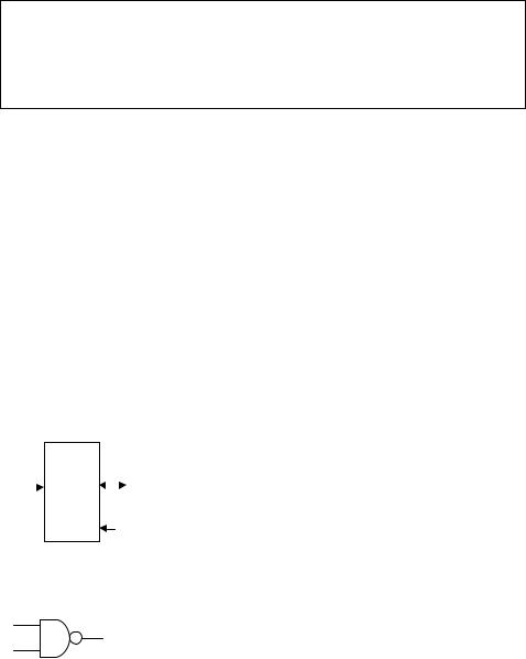
The mode of the signal can be IN, OUT, INOUT, or BUFFER. As illustrated in figure 2.3, IN and OUT are truly unidirectional pins, while INOUT is bidirectional. BUFFER, on the other hand, is employed when the output signal must be used (read) internally.
The type of the signal can be BIT, STD_LOGIC, INTEGER, etc. Data types will be discussed in detail in chapter 3.
Finally, the name of the entity can be basically any name, except VHDL reserved words (VHDL reserved words are listed in appendix E).
Example: Let us consider the NAND gate of figure 2.4. Its ENTITY can be specified as:
ENTITY nand_gate IS
PORT (a, b : IN BIT;
x : OUT BIT);
END nand_gate;
 OUT
OUT
IN |
|
Circuit |
|
INOUT |
|
|
|||
|
 BUFFER
Figure 2.3
Signal modes.
a
x
b
Figure 2.4
NAND gate.
TLFeBOOK

Code Structure |
17 |
The meaning of the ENTITY above is the following: the circuit has three I/O pins, being two inputs (a and b, mode IN) and one output (x, mode OUT). All three signals are of type BIT. The name chosen for the entity was nand_gate.
2.4ARCHITECTURE
The ARCHITECTURE is a description of how the circuit should behave (function). Its syntax is the following:
ARCHITECTURE architecture_name OF entity_name IS [declarations]
BEGIN (code)
END architecture_name;
As shown above, an architecture has two parts: a declarative part (optional), where signals and constants (among others) are declared, and the code part (from BEGIN down). Like in the case of an entity, the name of an architecture can be basically any name (except VHDL reserved words), including the same name as the entity’s.
Example: Let us consider the NAND gate of figure 2.4 once again.
ARCHITECTURE myarch OF nand_gate IS
BEGIN
x <= a NAND b;
END myarch;
The meaning of the ARCHITECTURE above is the following: the circuit must perform the NAND operation between the two input signals (a, b) and assign (‘‘<¼’’) the result to the output pin (x). The name chosen for this architecture was myarch. In this example, there is no declarative part, and the code contains just a single assignment.
2.5Introductory Examples
In this section, we will present two initial examples of VHDL code. Though we have not yet studied the constructs that appear in the examples, they will help illustrate fundamental aspects regarding the overall code structure. Each example is followed by explanatory comments and simulation results.
TLFeBOOK
18 |
Chapter 2 |
d |
|
|
|
q |
|
|
DFF
clk 

rst
Figure 2.5
DFF with asynchronous reset.
Example 2.1: DFF with Asynchronous Reset
Figure 2.5 shows the diagram of a D-type flip-flop (DFF), triggered at the risingedge of the clock signal (clk), and with an asynchronous reset input (rst). When rst ¼ ‘1’, the output must be turned low, regardless of clk. Otherwise, the output must copy the input (that is, q <¼ d) at the moment when clk changes from ‘0’ to ‘1’ (that is, when an upward event occurs on clk).
There are several ways of implementing the DFF of figure 2.5, one being the solution presented below. One thing to remember, however, is that VHDL is inherently concurrent (contrary to regular computer programs, which are sequential), so to implement any clocked circuit (flip-flops, for example) we have to ‘‘force’’ VHDL to be sequential. This can be done using a PROCESS, as shown below.
1 ---------------------------------------
2LIBRARY ieee;
3 USE ieee.std_logic_1164.all;
4 ---------------------------------------
5ENTITY dff IS
6PORT ( d, clk, rst: IN STD_LOGIC;
7 |
q: OUT STD_LOGIC); |
8 |
END dff; |
9 |
--------------------------------------- |
10 |
ARCHITECTURE behavior OF dff IS |
11BEGIN
12PROCESS (rst, clk)
13BEGIN
14IF (rst='1') THEN
15q <= '0';
16ELSIF (clk'EVENT AND clk='1') THEN
TLFeBOOK
Code Structure |
19 |
17q <= d;
18END IF;
19END PROCESS;
20END behavior;
21---------------------------------------
Comments:
Lines 2–3: Library declaration (library name and library use clause). Recall that the other two indispensable libraries (std and work) are made visible by default.
Lines 5–8: Entity d¤.
Lines 10–20: Architecture behavior.
Line 6: Input ports (input mode can only be IN). In this example, all input signals are of type STD_LOGIC.
Line 7: Output port (output mode can be OUT, INOUT, or BUFFER). Here, the output is also of type STD_LOGIC.
Lines 11–19: Code part of the architecture (from word BEGIN on).
Lines 12–19: A PROCESS (inside it the code is executed sequentially).
Line 12: The PROCESS is executed every time a signal declared in its sensitivity list changes. In this example, every time rst or clk changes the PROCESS is run.
Lines 14–15: Every time rst goes to ‘1’ the output is reset, regardless of clk (asynchronous reset).
Lines 16–17: If rst is not active, plus clk has changed (an EVENT occurred on clk), plus such event was a rising edge (clk ¼ ‘1’), then the input signal (d) is stored in the flip-flop (q <¼ d).
Lines 15 and 17: The ‘‘<¼’’ operator is used to assign a value to a SIGNAL. In contrast, ‘‘:¼’’ would be used for a VARIABLE. All ports in an entity are signals by default.
Lines 1, 4, 9, and 21: Commented out (recall that ‘‘- -’’ indicates a comment). Used only to better organize the design.
Note: VHDL is not case sensitive.
Simulation results:
Figure 2.6 presents simulation results regarding example 2.1. The graphs can be easily interpreted. The first column shows the signal names, as defined in the ENTITY. It also shows the mode (direction) of the signals; notice that the arrows associated
TLFeBOOK

20 |
Chapter 2 |
Figure 2.6
Simulation results of example 2.1.
a |
q |
|
b |
||
DFF |
||
|
||
clk |
|
|
Figure 2.7 |
|
|
DFF plus NAND gate. |
|
with rst, d, and clk are inward, and contain the letter I (input) inside, while that of q is outward and has an O (output) marked inside. The second column has the value of each signal in the position where the vertical cursor is placed. In the present case, the cursor is at 0ns, where the signals have value 1, 0, 0, 0, respectively. In this example, the values are simply ‘0’ or ‘1’, but when vectors are used, the values can be shown in binary, decimal, or hexadecimal form. The third column shows the simulation proper. The input signals (rst, d, clk) can be chosen freely, and the simulator will determine the corresponding output (q). Comparing the results of figure 2.6 with those expected from the circuit shown previously, we notice that it works properly. As mentioned earlier, the designs presented in the book were synthesized onto CPLD/ FPGA devices (appendix A), either from Altera or Xilinx. The tools used were either ISE combined with ModelSim (for Xilinx chips—appendix B), or MaxPlus II combined with Advanced Synthesis Software (for Altera CPLDs—appendix C), or Quartus II (also for Altera devices—appendix D). Leonardo Spectrum (from Mentor Graphics) was also used occasionally.
Example 2.2: DFF plus NAND Gate
The circuit of figure 2.4 was purely combinational, while that of figure 2.5 was purely sequential. The circuit of figure 2.7 is a mixture of both (without reset). In the
TLFeBOOK

Code Structure |
21 |
Figure 2.8
Simulation results of example 2.2.
solution that follows, we have purposely introduced an unnecessary signal (temp), just to illustrate how a signal should be declared. Simulation results from the circuit synthesized with the code below are shown in figure 2.8.
1 ---------------------------------------
2ENTITY example IS
3PORT ( a, b, clk: IN BIT;
4 |
q: OUT BIT); |
5 |
END example; |
6 |
--------------------------------------- |
7 |
ARCHITECTURE example OF example IS |
8 |
SIGNAL temp : BIT; |
9BEGIN
10temp <= a NAND b;
11PROCESS (clk)
12BEGIN
13IF (clk'EVENT AND clk='1') THEN q<=temp;
14END IF;
15END PROCESS;
16END example;
17 ---------------------------------------
Comments:
Library declarations are not necessary in this case, because the data is of type BIT, which is specified in the library std (recall that the libraries std and work are made visible by default).
Lines 2–5: Entity example.
Lines 7–16: Architecture example.
TLFeBOOK

22 |
Chapter 2 |
Line 3: Input ports (all of type BIT).
Line 4: Output port (also of type BIT).
Line 8: Declarative part of the architecture (optional). The signal temp, of type BIT, was declared. Notice that there is no mode declaration (mode is only used in entities).
Lines 9–15: Code part of the architecture (from word BEGIN on).
Lines 11–15: A PROCESS (sequential statements executed every time the signal clk changes).
Lines 10 and 11–15: Though within a process the execution is sequential, the process, as a whole, is concurrent with the other (external) statements; thus line 10 is executed concurrently with the block 11–15.
Line 10: Logical NAND operation. Result is assigned to signal temp.
Lines 13–14: IF statement. At the rising edge of clk the value of temp is assigned to q.
Lines 10 and 13: The ‘‘<¼’’ operator is used to assign a value to a SIGNAL. In contrast, ‘‘:¼’’ would be used for a VARIABLE.
Lines 8 and 10: Can be eliminated, changing ‘‘q <¼ a NAND b’’ in line 13.
Lines 1, 6, and 17: Commented out. Used only to better organize the design.
2.6 Problems
Problem 2.1: Multiplexer
The top-level diagram of a multiplexer is shown in figure P2.1. According to the truth table, the output should be equal to one of the inputs if sel ¼ ‘‘01’’ (c ¼ a) or sel ¼ ‘‘10’’ (c ¼ b), but it should be ‘0’ or Z (high impedance) if sel ¼ ‘‘00’’ or sel ¼ ‘‘11’’, respectively.
a (7:0) |
|
|
|
|
sel |
c |
||||
|
|
|
||||||||
c (7:0) |
00 |
0 |
||||||||
|
|
|
|
MUX |
|
|||||
b (7:0) |
|
|
|
|
01 |
a |
||||
|
||||||||||
|
|
|
|
|
|
|
||||
|
|
|
10 |
b |
||||||
|
|
|||||||||
|
|
|
|
|
|
|
|
11 |
Z |
|
|
|
|
|
|
|
|
|
|||
|
|
|
|
sel (1:0) |
|
|||||
|
|
|
|
|
|
|
||||
Figure P2.1
TLFeBOOK
Code Structure |
23 |
a)Complete the VHDL code below.
b)Write relevant comments regarding your solution (as in examples 2.1 and 2.2).
c)Compile and simulate your solution, checking whether it works as expected.
Note: A solution using IF was employed in the code below, because it is more intuitive. However, as will be seen later, a multiplexer can also be implemented with other statements, like WHEN or CASE.
1 ---------------------------------------
2LIBRARY ieee;
3 USE _________________________ ;
4 ---------------------------------------
5ENTITY mux IS
6PORT ( __ , __ : ___ STD_LOGIC_VECTOR (7 DOWNTO 0);
7sel : IN ____________________________ ;
8 |
___ : OUT STD_LOGIC_VECTOR (7 DOWNTO 0)); |
9 |
END _____ ; |
10 |
--------------------------------------- |
11 |
ARCHITECTURE example OF _____ IS |
12BEGIN
13PROCESS (a, b, ____ )
14BEGIN
15IF (sel = "00") THEN
16c <= "00000000";
17ELSIF (__________) THEN
18c <= a;
19_____ (sel = "10") THEN
20c <= __;
21ELSE
22c <= (OTHERS => '__');
23END ___ ;
24END _________ ;
25END _________ ;
26 ---------------------------------------
TLFeBOOK

24 |
Chapter 2 |
a |
d |
b
c
Figure P2.2
Problem 2.2: Logic Gates
a)Write a VHDL code for the circuit of figure P2.2. Notice that it is purely combinational, so a PROCESS is not necessary. Write an expression for d using only logical operators (AND, OR, NAND, NOT, etc.).
b)Synthesize and simulate your circuit. After assuring that it works properly, open the report file and check the actual expression implemented by the compiler. Compare it with your expression.
TLFeBOOK