

12 Additional System Designs
In this chapter, additional designs are presented, with the purpose of further illustrating the usage of the VHDL units that are intended for system-level design: PACKAGES, COMPONENTS, FUNCTIONS, and PROCEDURES.
12.1Serial-Parallel Multiplier
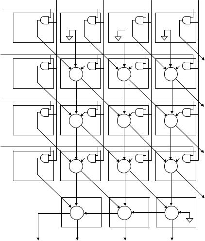
Figure 12.1 shows the RTL diagram of a serial-parallel multiplier. One of the input vectors (a) is applied serially to the circuit (one bit at a time, starting from the LSB), while the other (b) is applied in parallel (all bits simultaneously). Say that a has M bits, while b has N. Then, after all M bits of a have been presented to the system, a string of M ‘0’s must follow, in order to complete the (M þ N)-bit output product.
As can be seen in figure 12.1, the system is pipelined, and is constructed using AND gates, full-adder units, plus registers (flip-flops). Each unit of the pipeline (except the leftmost one) requires one adder and two registers, plus an AND gate to compute one of the inputs. Thus for an M N multiplier, O(N) of such units are required.
The solution presented below is of structural type (only COMPONENTS were used). Notice that there is more than one level of instantiation (the unit called pipe instantiates other components, while in the final code, pipe is instantiated as well (besides other components).
The design of each component is shown below, along with the PACKAGE containing all COMPONENT declarations, followed by the project proper (main code). Simulation results were also included.
1 ------ and_2.vhd (component): ---------
2LIBRARY ieee;
3 USE ieee.std_logic_1164.all;
4 ---------------------------------------
5ENTITY and_2 IS
6PORT ( a, b: IN STD_LOGIC;
7 |
y: OUT STD_LOGIC); |
8 |
END and_2; |
9 |
--------------------------------------- |
10 |
ARCHITECTURE and_2 OF and_2 IS |
11BEGIN
12y <= a AND b;
13END and_2;
14 ---------------------------------------
TLFeBOOK

276 |
Chapter 12 |
b(3) |
|
b(2) |
|
b(1) |
|
b(0) |
|
|
a |
|
|
|
|
|
|
|
|
a(0) |
|
+ |
|
+ |
|
+ |
|
prod |
a(1) |
D |
D |
D |
D |
||||
a(2) |
|
|
|
|
|
|
|
|
a(3) |
|
D |
|
D |
|
D |
|
|
|
|
|
|
|
|
Figure 12.1
Serial-parallel multiplier.
1 ------ reg.vhd (component): -----------
2LIBRARY ieee;
3 USE ieee.std_logic_1164.all;
4 ---------------------------------------
5ENTITY reg IS
6PORT ( d, clk, rst: IN STD_LOGIC;
7 |
q: OUT STD_LOGIC); |
8 |
END reg; |
9 |
--------------------------------------- |
10 |
ARCHITECTURE reg OF reg IS |
11BEGIN
12PROCESS (clk, rst)
13BEGIN
14IF (rst='1') THEN q<='0';
15ELSIF (clk'EVENT AND clk='1') THEN q<=d;
16END IF;
17END PROCESS;
18END reg;
19 |
--------------------------------------- |
1 ------ |
fau.vhd (component): ----------- |
2LIBRARY ieee;
3 USE ieee.std_logic_1164.all;
4 ---------------------------------------
5 ENTITY fau IS
TLFeBOOK
Additional System Designs |
277 |
6PORT ( a, b, cin: IN STD_LOGIC;
7 |
s, cout: OUT STD_LOGIC); |
8 |
END fau; |
9 |
--------------------------------------- |
10 |
ARCHITECTURE fau OF fau IS |
11BEGIN
12s <= a XOR b XOR cin;
13cout <= (a AND b) OR (a AND cin) OR (b AND cin);
14END fau;
15 |
--------------------------------------- |
1 ------ ---------- |
pipe.vhd (component): |
2LIBRARY ieee;
3 USE ieee.std_logic_1164.all;
4 USE work.my_components.all;
5 ---------------------------------------
6ENTITY pipe IS
7PORT ( a, b, clk, rst: IN STD_LOGIC;
8 |
q: OUT STD_LOGIC); |
9 |
END pipe; |
10 |
--------------------------------------- |
11 |
ARCHITECTURE structural OF pipe IS |
12SIGNAL s, cin, cout: STD_LOGIC;
13BEGIN
14U1: COMPONENT fau PORT MAP (a, b, cin, s, cout);
15U2: COMPONENT reg PORT MAP (cout, clk, rst, cin);
16U3: COMPONENT reg PORT MAP (s, clk, rst, q);
17END structural;
18 ---------------------------------------
1----- my_components.vhd (package):-----
2LIBRARY ieee;
3 USE ieee.std_logic_1164.all;
4 ---------------------------------------
5 PACKAGE my_components IS
6 --------------------------
7COMPONENT and_2 IS
8 PORT (a, b: IN STD_LOGIC; y: OUT STD_LOGIC);
TLFeBOOK
278 |
Chapter 12 |
9 END COMPONENT;
10 --------------------------
11 COMPONENT fau IS
12PORT (a, b, cin: IN STD_LOGIC; s, cout: OUT STD_LOGIC);
13END COMPONENT;
14 --------------------------
15 COMPONENT reg IS
16PORT (d, clk, rst: IN STD_LOGIC; q: OUT STD_LOGIC);
17END COMPONENT;
18 --------------------------
19 COMPONENT pipe IS
20PORT (a, b, clk, rst: IN STD_LOGIC; q: OUT STD_LOGIC);
21END COMPONENT;
22 --------------------------
23 END my_components;
24 ---------------------------------------
1 ----- multiplier.vhd (project): -------
2LIBRARY ieee;
3 USE ieee.std_logic_1164.all;
4 USE work.my_components.all;
5 ---------------------------------------
6ENTITY multiplier IS
7PORT ( a, clk, rst: IN STD_LOGIC;
8b: IN STD_LOGIC_VECTOR (3 DOWNTO 0);
9 |
prod: OUT STD_LOGIC); |
10 |
END multiplier; |
11 |
--------------------------------------- |
12 |
ARCHITECTURE structural OF multiplier IS |
13SIGNAL and_out, reg_out: STD_LOGIC_VECTOR (3 DOWNTO 0);
14BEGIN
15U1: COMPONENT and_2 PORT MAP (a, b(3), and_out(3));
16U2: COMPONENT and_2 PORT MAP (a, b(2), and_out(2));
17U3: COMPONENT and_2 PORT MAP (a, b(1), and_out(1));
18U4: COMPONENT and_2 PORT MAP (a, b(0), and_out(0));
19U5: COMPONENT reg PORT MAP (and_out(3), clk, rst,
20reg_out(3));
TLFeBOOK
Additional System Designs |
279 |
Figure 12.2
Simulation results of serial-parallel multiplier.
21U6: COMPONENT pipe PORT MAP (and_out(2), reg_out(3),
22clk, rst, reg_out(2));
23U7: COMPONENT pipe PORT MAP (and_out(1), reg_out(2),
24clk, rst, reg_out(1));
25U8: COMPONENT pipe PORT MAP (and_out(0), reg_out(1),
26clk, rst, reg_out(0));
27prod <= reg_out(0);
28END structural;
29---------------------------------------
Simulation results are shown in figure 12.2. a ¼ ‘‘1100’’ (decimal 12) was applied to the serial input. Notice that this input must start with the LSB (a(0) ¼ ‘0’), which appears in the time slot 100 ns–200 ns, while the MSB (a(3) ¼ ‘1’) is situated in 400 ns–500 ns. Recall that four zeros must then follow. On the other hand, at the parallel input, b ¼ ‘‘1101’’ (decimal 13) was applied. The expected result, prod ¼ ‘‘10011100’’ (decimal 156), can be observed in the lower plot. Recall that the first bit out is the LSB; that is, prod(0) ¼ ‘0’, which appears in the time slot immediately after the first rising edge of clock; (that is, 150 ns–250 ns), while the last bit (MSB) of prod is situated in 850 ns–950 ns.
12.2Parallel Multiplier
Figure 12.3 shows the diagram of a 4-bit parallel multiplier. Contrary to the case of figure 12.1, here all input bits are applied to the system simultaneously. Therefore, registers are not required. Notice in figure 12.3 that only AND gates and FAU (full adder units) are necessary to construct a parallel multiplier. The operands are a and b (each of four bits), and the resulting product is prod (eight bits).
TLFeBOOK
280 |
|
|
|
Chapter 12 |
b(3) |
|
b(2) |
b(1) |
b(0) |
a(0) |
|
|
|
|
a(1) |
|
|
|
p(0) |
|
|
|
|
|
+ |
|
+ |
|
+ |
carry |
sum |
|
|
|
a(2) |
|
|
|
p(1) |
|
|
|
|
|
+ |
|
+ |
|
+ |
a(3) |
|
|
|
|
|
|
|
|
p(2) |
+ |
|
+ |
|
+ |
|
|
|
|
p(3) |
+ |
+ |
|
+ |
|
p(7) |
p(6) |
p(5) |
|
p(4) |
Figure 12.3
Parallel multiplier.
TLFeBOOK

Additional System Designs |
281 |
Figure 12.4
Simulation results of parallel multiplier.
The VHDL code shown below was based on COMPONENT instantiation. Notice that two basic components, AND_2 and FAU, were first specified (shown in section 12.1). These components were then instantiated to construct higher-level components, top_row, mid_row, and lower_row. All of these components were then declared in a PACKAGE called my_components, and finally used in the project called multiplier to implement the circuit of figure 12.3. Simulation results are shown in figure 12.4.
1 ------- top_row.vhd (component): -------------
2LIBRARY ieee;
3 USE ieee.std_logic_1164.all;
4 USE work.my_components.all;
5 ---------------------------------------
6ENTITY top_row IS
7PORT ( a: IN STD_LOGIC;
8b: IN STD_LOGIC_VECTOR (3 DOWNTO 0);
9sout, cout: OUT STD_LOGIC_VECTOR (2 DOWNTO 0);
10p: OUT STD_LOGIC);
11END top_row;
12 ---------------------------------------
13 ARCHITECTURE structural OF top_row IS
14BEGIN
15U1: COMPONENT and_2 PORT MAP (a, b(3), sout(2));
16U2: COMPONENT and_2 PORT MAP (a, b(2), sout(1));
17U3: COMPONENT and_2 PORT MAP (a, b(1), sout(0));
18U4: COMPONENT and_2 PORT MAP (a, b(0), p);
19cout(2)<='0'; cout(1)<='0'; cout(0)<='0';
20END structural;
21 ----------------------------------------------
TLFeBOOK
282 |
Chapter 12 |
1 ------- mid_row.vhd (component): -------------
2LIBRARY ieee;
3 USE ieee.std_logic_1164.all;
4 USE work.my_components.all;
5 ---------------------------------------
6ENTITY mid_row IS
7PORT ( a: IN STD_LOGIC;
8b: IN STD_LOGIC_VECTOR (3 DOWNTO 0);
9sin, cin: IN STD_LOGIC_VECTOR (2 DOWNTO 0);
10sout, cout: OUT STD_LOGIC_VECTOR (2 DOWNTO 0);
11p: OUT STD_LOGIC);
12END mid_row;
13 ---------------------------------------
14 ARCHITECTURE structural OF mid_row IS
15SIGNAL and_out: STD_LOGIC_VECTOR (2 DOWNTO 0);
16BEGIN
17U1: COMPONENT and_2 PORT MAP (a, b(3), sout(2));
18U2: COMPONENT and_2 PORT MAP (a, b(2), and_out(2));
19U3: COMPONENT and_2 PORT MAP (a, b(1), and_out(1));
20U4: COMPONENT and_2 PORT MAP (a, b(0), and_out(0));
21U5: COMPONENT fau PORT MAP (sin(2), cin(2), and_out(2),
22sout(1), cout(2));
23U6: COMPONENT fau PORT MAP (sin(1), cin(1), and_out(1),
24sout(0), cout(1));
25U7: COMPONENT fau PORT MAP (sin(0), cin(0), and_out(0),
26p, cout(0));
27END structural;
28 ----------------------------------------------
1 ------- lower_row.vhd (component): -----------
2LIBRARY ieee;
3 USE ieee.std_logic_1164.all;
4 USE work.my_components.all;
5 ---------------------------------------
6ENTITY lower_row IS
7PORT ( sin, cin: IN STD_LOGIC_VECTOR (2 DOWNTO 0);
8 |
p: OUT STD_LOGIC_VECTOR (3 DOWNTO 0); |
9 |
END lower_row; |
10 |
--------------------------------------- |
TLFeBOOK
Additional System Designs |
283 |
11 ARCHITECTURE structural OF lower_row IS
12SIGNAL local: STD_LOGIC_VECTOR (2 DOWNTO 0);
13BEGIN
14local(0)<='0';
15U1: COMPONENT fau PORT MAP (sin(0), cin(0), local(0),
16p(0), local(1));
17U2: COMPONENT fau PORT MAP (sin(1), cin(1), local(1),
18p(1), local(2));
19U3: COMPONENT fau PORT MAP (sin(2), cin(2), local(2),
20p(2), p(3));
21END structural;
22 ----------------------------------------------
1 ----- my_components.vhd (package): -----------
2LIBRARY ieee;
3 USE ieee.std_logic_1164.all;
4 ------------------------------------
5 PACKAGE my_components IS
6 -----------------------
7COMPONENT and_2 IS
8 |
PORT ( a, b: IN STD_LOGIC; y: OUT STD_LOGIC); |
|
9 |
END COMPONENT; |
|
10 |
----------------------- |
|
11 |
COMPONENT fau IS |
-- full adder unit |
12PORT ( a, b, cin: IN STD_LOGIC; s, cout: OUT STD_LOGIC);
13END COMPONENT;
14 -----------------------
15COMPONENT top_row IS
16PORT ( a: IN STD_LOGIC;
17 |
b: IN STD_LOGIC_VECTOR (3 DOWNTO |
0); |
18 |
sout, cout: OUT STD_LOGIC_VECTOR |
(2 DOWNTO 0); |
19 |
p: OUT STD_LOGIC); |
|
20 |
END COMPONENT; |
|
21 |
----------------------- |
|
22COMPONENT mid_row IS
23PORT ( a: IN STD_LOGIC;
24 |
b: IN STD_LOGIC_VECTOR (3 DOWNTO |
0); |
25 |
sin, cin: IN STD_LOGIC_VECTOR (2 |
DOWNTO 0); |
26 |
sout, cout: OUT STD_LOGIC_VECTOR |
(2 DOWNTO 0); |
TLFeBOOK
284 |
Chapter 12 |
27 |
p: OUT STD_LOGIC); |
28 |
END COMPONENT; |
29 |
----------------------- |
30COMPONENT lower_row IS
31PORT ( sin, cin: IN STD_LOGIC_VECTOR (2 DOWNTO 0);
32 |
p: OUT STD_LOGIC_VECTOR (3 DOWNTO 0); |
33 |
END COMPONENT; |
34 |
----------------------- |
35 |
END my_components; |
36 |
---------------------------------------------- |
1 |
------- multiplier.vhd (project): ------------ |
2LIBRARY ieee;
3 USE ieee.std_logic_1164.all;
4 USE work.my_components.all;
5 ---------------------------------------
6ENTITY multiplier IS
7PORT ( a, b: IN STD_LOGIC_VECTOR (3 DOWNTO 0);
8 |
prod: OUT STD_LOGIC_VECTOR (7 DOWNTO 0)); |
9 |
END multiplier; |
10 |
--------------------------------------- |
11 |
ARCHITECTURE structural OF multiplier IS |
12TYPE matrix IS ARRAY (0 TO 3) OF
13STD_LOGIC_VECTOR (2 DOWNTO 0);
14SIGNAL s, c: matrix;
15BEGIN
16U1: COMPONENT top_row PORT MAP (a(0), b, s(0), c(0),
17prod(0));
18U2: COMPONENT mid_row PORT MAP (a(1), b, s(0), c(0), s(1),
19c(1), prod(1));
20U3: COMPONENT mid_row PORT MAP (a(2), b, s(1), c(1), s(2),
21c(2), prod(2));
22U4: COMPONENT mid_row PORT MAP (a(3), b, s(2), c(2), s(3),
23c(3), prod(3));
24U5: COMPONENT lower_row PORT MAP (s(3), c(3),
25prod(7 DOWNTO 4));
26END structural;
27 ----------------------------------------------
TLFeBOOK
Additional System Designs |
285 |
||||||
|
|
|
|
|
|
|
|
|
|
|
|
|
|
|
|
|
|
|
|
|
|
|
|
|
|
|
|
|
|
|
|
|
|
|
|
|
|
|
|
|
|
|
|
|
|
|
|
|
|
|
|
|
|
|
|
Figure 12.5
Parallel multiplier inferred from the pre-defined ‘‘*’’ operator.
A Simpler Approach
The example above had the purpose of exploring several aspects related to system design using VHDL. However, for the particular case of a parallel multiplier, it can be immediately inferred by means of the pre-defined ‘‘*’’ (multiplication) operator. Therefore, the circuit above can be represented using the compact form of figure 12.5, and the whole code above can be replaced by the following code:
1 ---------------------------------------
2LIBRARY ieee;
3 USE ieee.std_logic_1164.all;
4 USE ieee.std_logic_arith.all;
5 ---------------------------------------
6ENTITY multiplier3 IS
7PORT ( a, b: IN SIGNED(3 DOWNTO 0);
8 |
prod: OUT SIGNED(7 DOWNTO 0)); |
9 |
END multiplier3; |
10 |
--------------------------------------- |
11 |
ARCHITECTURE behavior OF multiplier3 IS |
12BEGIN
13prod <= a * b;
14END behavior;
15 ---------------------------------------
12.3Multiply-Accumulate Circuits
Multiplication followed by accumulation is a common operation in many digital systems, particularly those highly interconnected, like digital filters, neural networks, data quantizers, etc.
TLFeBOOK
286 |
|
|
|
|
|
|
|
|
|
|
|
|
Chapter 12 |
|
|
|
|
|
|
|
|
|
|
|
|
|
|
|
|
|
|
|
|
|
|
|
|
|
|
|
|
|
|
|
|
|
|
|
|
|
|
|
|
|
|
|
|
|
|
|
|
|
|
|
|
|
|
|
|
|
|
|
|
|
|
|
|
|
|
|
|
|
|
|
|
|
|
|
|
|
|
|
|
|
|
|
|
|
|
|
|
|
|
|
|
|
|
|
|
|
|
|
|
|
|
|
|
|
|
|
|
|
|
|
|
|
|
|
|
|
|
|
|
|
|
|
|
|
|
|
|
|
|
|
|
|
|
|
|
|
|
|
|
|
|
|
|
|
|
|
|
|
|
|
|
|
|
|
|
|
|
|
|
|
|
|
|
|
|
|
|
Figure 12.6
MAC circuit.
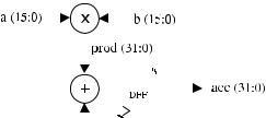
One typical MAC (multiply-accumulate) architecture is illustrated in figure 12.6. It consists of multiplying two values, then adding the result to the previously accumulated value, which must then be re-stored in the registers for future accumulations. Another feature of a MAC circuit is that it must check for overflow, which might happen when the number of MAC operations is large.
This design can be done using COMPONENTS, because we have already designed each of the units shown in figure 12.6. However, since it is a relatively simple circuit, it can also be designed directly. The latter approach is illustrated below, while the former is treated in problem 12.2. In any case, the MAC circuit, as a whole, can be used as a COMPONENT in applications like digital filters and neural networks (next sections).
Overflow: In the implementation (code) shown below, a FUNCTION was written to detect overflow and truncate the result in case overflow happens. Overflow in a signed adder occurs when two operands with the same signal (leftmost bit) produce a result with a di¤erent signal from them. If it occurs, the largest value (positive or negative) should be assigned to the result. For example, if eight bits are used to encode the values, the addition of two positive numbers must fall in the interval from 0 to 127, while the addition of two negative numbers must fall between 128 (that is, þ128 in unsigned representation) and 1 (255 in unsigned representation). For example, 65 þ 65 ¼ 130, which is indeed 126 (overflow), so the result should be truncated to the largest positive value (127). Likewise, ( 70) þ ( 70) ¼ 140, which is, indeed, 116 (overflow), so the result should be truncated to the most negative value ( 128). On the other hand, when the operands have di¤erent signals, overflow cannot happen.
The add_truncate( ) function was placed in a PACKAGE (chapter 10) called my_functions. The function receives two signals, adds them, then checks for overflow
TLFeBOOK
Additional System Designs |
287 |
and truncates the result if necessary, returning the processed result to the main code. Notice that the function is generic, for the number of bits of the operands is passed to it by means of a parameter called size. Notice also in the main code that the parameters passed to the function were declared as signals (line 14), because variables are not allowed (chapter 11).
1 ------- PACKAGE my_functions: -----------------------------
2LIBRARY ieee;
3 USE ieee.std_logic_1164.all;
4 USE ieee.std_logic_arith.all;
5 ----------------------------------------------------------
6PACKAGE my_functions IS
7 FUNCTION add_truncate (SIGNAL a, b: SIGNED; size: INTEGER) 8 RETURN SIGNED;
9 END my_functions;
10 ----------------------------------------------------------
11 PACKAGE BODY my_functions IS
12FUNCTION add_truncate (SIGNAL a, b: SIGNED; size: INTEGER)
13RETURN SIGNED IS
14VARIABLE result: SIGNED (7 DOWNTO 0);
15BEGIN
16result := a + b;
17IF (a(a'left)=b(b'left)) AND
18(result(result'LEFT)/=a(a'left)) THEN
19result := (result'LEFT => a(a'LEFT),
20 |
OTHERS => NOT a(a'left)); |
21END IF;
22RETURN result;
23END add_truncate;
24END my_functions;
25 |
---------------------------------------------------------- |
1 ------- ----------------------- |
Main code: |
2LIBRARY ieee;
3 USE ieee.std_logic_1164.all;
4 USE ieee.std_logic_arith.all;
5 USE work.my_functions.all;
6 ------------------------------------------
TLFeBOOK

288 |
Chapter 12 |
7ENTITY mac IS
8PORT ( a, b: IN SIGNED(3 DOWNTO 0);
9clk, rst: IN STD_LOGIC;
10acc: OUT SIGNED(7 DOWNTO 0));
11END mac;
12------------------------------------------
13ARCHITECTURE rtl OF mac IS
14SIGNAL prod, reg: SIGNED(7 DOWNTO 0);
15BEGIN
16PROCESS (rst, clk)
17VARIABLE sum: SIGNED(7 DOWNTO 0);
18BEGIN
19prod <= a * b;
20IF (rst='1') THEN
21reg <= (OTHERS=>'0');
22ELSIF (clk'EVENT AND clk='1') THEN
23sum := add_truncate (prod, reg, 8);
24reg <= sum;
25END IF;
26acc <= reg;
27END PROCESS;
28END rtl;
29------------------------------------------
Simulation results are presented in figure 12.7. Notice that the following sequence of signals was presented to the MAC circuit: a ¼ (0, 2, 4, 6, 8, 6, 4, 2), b ¼ (0, 3, 6, 7, 8, 8, 8). Therefore, the expected output sequence is acc ¼ (0, 6, 30,12, 52, 100, 148) (recall that 12 is represented in the graph as 256 12 ¼ 244).
Figure 12.7
Simulation results of MAC circuit.
TLFeBOOK
Additional System Designs |
289 |
All the values are OK, except the last one, for it is above the maximum positive value allowed for 8-bit signed numbers (127). Therefore, this result was kept at 127.
12.4Digital Filters
Digital signal processing (DSP) finds innumerable applications in the fields of audio, video, and communications, among others. Such applications are generally based on LTI (linear time invariant) systems, which can be implemented with digital circuitry.
Any LTI system be represented by the following equation:
NM
aky[n k] ¼ |
bkx[n k] |
k¼0 |
k¼0 |
where ak and bk are the filter coe‰cients, and x[n k], y[n k] are the current (for k ¼ 0) and earlier (for k > 0) input and output values, respectively. To implement this expression, registers are necessary to store x[n k] and/or y[n k] (for k > 0), besides multipliers and adders, which are well-known building blocks in the digital domain.
The impulse response of a digital filter can be divided into two categories: IIR (infinite impulse response) and FIR (finite impulse response). The former corresponds to the general case described by the equation above, while the latter occurs when N ¼ 0. Only FIR filters can exhibit linear phase, so they are indispensable when linear phase is required, like in many telecom applications. With N ¼ 0, the equation above becomes
M
y[n] ¼ ckx[n k]
k¼0
where ck ¼ bk/a0 are the coe‰cients of the FIR filter. This equation can be implemented by the system of figure 12.8, where D (delay) represents a register (flip-flops), a triangle is a multiplier, and a circle means an adder.
An equivalent RTL representation is shown in figure 12.9. As shown, the values of x are stored in a shift register, whose outputs are connected to multipliers and then to adders. The coe‰cients must also be stored on chip. However, if the coe‰cients are always the same (that is, if it is a dedicated filter), their values can be implemented by means of logic gates rather than registers (we just need to store CONSTANTS). On the other hand, if it is a general purpose filter, then registers are required for the coe‰cients. In the architecture of figure 12.9, the output vector (y) was also stored, in order to provide a clean, synchronous output.
TLFeBOOK

290 |
Chapter 12 |
x[n] |
+ |
y[n] |
|
co |
|
|
D |
|
x[n-1] |
+ |
|
c1
D
x[n-2] 
 + c2
+ c2
D
x[n-3]
c3
Figure 12.8
FIR filter diagram (with 4 coe‰cients).
Figure 12.9
RTL representation of a FIR filter.
The circuit of figure 12.9 can be constructed in several ways. However, if it is intended for future reuse or sharing, than it should be as generic as possible. In the code presented below, two GENERIC parameters are specified (line 7): n defines the number of filter coe‰cients, while m specifies the number of bits used to represent the input and coe‰cients. For the output, 2 m bits were used. Thus, for example, 16 bits could be used for x, coef, and reg, while 32 bits could be used for all other signals (from the outputs of the multipliers all the way to y).
Notice that the lower section of the filter contains a MAC (multiply-accumulate) pipeline. This circuit is closely related to the MAC circuit discussed in section 12.3. Here too, overflow can happen, so an add/truncate procedure must be included in the design.
TLFeBOOK
Additional System Designs |
291 |
In the solution below, the coe‰cients were considered as CONSTANTS (line 19), thus inferring no flip-flops. The values chosen were coef(0) ¼ 4, coef(1) ¼ 3, coef(2) ¼ 2, and coef(3) ¼ 1. Small values were chosen for n and m (4 for both) in order to make the simulation results easy to visualize. With n ¼ m ¼ 4, the synthesized circuit required 20 flip-flops (four for each stage of the shift register, plus eight for the output). As described in chapter 7, flip-flops are inferred when a signal assignment is made on the transition of another signal, which occurs in lines 33–45 of the code below (notice that indeed VARIABLE assignments are made in lines 33–38, but since their values are then passed to a SIGNAL (y), registers are inferred).
1 -----------------------------------------------------------
2LIBRARY ieee;
3USE ieee.std_logic_1164.all;
4 |
USE ieee.std_logic_arith.all; -- package needed for SIGNED |
5 |
----------------------------------------------------------- |
6ENTITY fir2 IS
7GENERIC (n: INTEGER := 4; m: INTEGER := 4);
8-- n = # of coef., m = # of bits of input and coef.
9 -- Besides n and m, CONSTANT (line 19) also need adjust
10PORT ( x: IN SIGNED(m-1 DOWNTO 0);
11clk, rst: IN STD_LOGIC;
12y: OUT SIGNED(2*m-1 DOWNTO 0));
13END fir2;
14 |
----------------------------------------------------------- |
|
15 |
ARCHITECTURE rtl OF fir2 IS |
|
16 |
TYPE registers IS ARRAY (n-2 DOWNTO 0) OF |
|
17 |
SIGNED(m-1 DOWNTO |
0); |
18 |
TYPE coefficients IS ARRAY (n-1 DOWNTO 0) |
OF |
19 |
SIGNED(m-1 DOWNTO 0); |
|
20SIGNAL reg: registers;
21CONSTANT coef: coefficients := ("0001", "0010", "0011",
22 |
"0100"); |
23BEGIN
24PROCESS (clk, rst)
25VARIABLE acc, prod:
26SIGNED(2*m-1 DOWNTO 0) := (OTHERS=>'0');
27VARIABLE sign: STD_LOGIC;
28BEGIN
29----- reset: --------------------------
TLFeBOOK

292 |
Chapter 12 |
30IF (rst='1') THEN
31FOR i IN n-2 DOWNTO 0 LOOP
32FOR j IN m-1 DOWNTO 0 LOOP
33 |
reg(i)(j) <= '0'; |
34END LOOP;
35END LOOP;
36----- register inference + MAC: -------
37ELSIF (clk'EVENT AND clk='1') THEN
38acc := coef(0)*x;
39FOR i IN 1 TO n-1 LOOP
40sign := acc(2*m-1);
41prod := coef(i)*reg(n-1-i);
42acc := acc + prod;
43---- overflow check: ------------
44IF (sign=prod(prod'left)) AND
45 |
(acc(acc'left) /= sign) |
46 |
THEN |
47 |
acc := (acc'LEFT => sign, OTHERS => NOT sign); |
48END IF;
49END LOOP;
50reg <= x & reg(n-2 DOWNTO 1);
51END IF;
52y <= acc;
53END PROCESS;
54END rtl;
55-----------------------------------------------------------
Simulation results are shown in figure 12.10. Recall that the coe‰cients are coef(0) ¼ 4, coef(1) ¼ 3, coef(2) ¼ 2, and coef(3) ¼ 1, and that the numbers are
Figure 12.10
Simulation results of FIR filter of figure 12.9.
TLFeBOOK

Additional System Designs |
293 |
SIGNED (therefore, with 4-bit values, the range is from 8 to þ7). The sequence applied to the input was x[0] ¼ 0, x[1] ¼ 5, x[2] ¼ 6 (16 6 ¼ 10 in the graph), x[3] ¼ 1 (16 1 ¼ 15 in the graph), x[4] ¼ 4, x[5] ¼ 7 (16 7 ¼ 9 in the graph), and x[6] ¼ 2 (16 2 ¼ 14 in the graph). Therefore, with all flip-flops previously reset, at the first positive edge of clk the expected output is y[0] ¼ coef(0)*x[0] ¼ 0, which coincides with the first result for y in figure 12.10. At the next upward transition of clk, the expected value is y[1] ¼ coef(0)*x[1] þ coef(1)*x[0] ¼ 20. And one clock cycle later, y[1] ¼ coef(0)*x[2] þ coef(1)*x[1] þ coef(2)*x[0] ¼ 9 (256 9 ¼ 247 in the graph), and so on.
General Purpose FIR Filter
The design presented above contained fixed coe‰cients, and is therefore adequate for an ASIC with a dedicated filter. For a general purpose implementation (that is, with programmable coe‰cients), the architecture of figure 12.11 can be used instead. As can be seen, this structure is modular and allows several chips to be cascaded, which might be helpful in some applications, because FIR filters tend to have many taps (coe‰cients).
In this structure, there are two shift registers, one for storing the inputs (x) and the other for the coe‰cients (coef ). The structure is divided into n equal modules, called TAP1, . . . , TAPn. Each module (TAP) contains a slice of the shift registers, plus a multiplier and an adder. It also contains an output register, but this is optional (could be used at the last TAP only). This would, however, increase the ripple propagation
Figure 12.11
General purpose FIR filter.
TLFeBOOK

294 |
Chapter 12 |
x1 |
|
w11 |
y1 |
||||
|
|
|
|
1 |
|
||
|
|
||||||
|
|
|
|
||||
|
|
w12 |
|
|
|||
|
|
|
|
|
|||
|
w13 |
|
|||||
x2 |
|
|
|
|
2 |
|
y2 |
|
|
||||||
Input |
Hidden layers |
Output layer |
x3 |
3 |
y3 |
(a) |
(b) |
Figure 12.12
Feedforward neural network.
between the adders. Of course, all coe‰cients must be loaded before the computation starts. This FIR architecture will be object of problem 12.4.
12.5 Neural Networks
Neural Networks (NN) are highly parallel, highly interconnected systems. Such characteristics make their implementation very challenging, and also very costly, due to the large amount of hardware required.
A feedforward NN is shown in figure 12.12(a). In this example, the circuit has three layers, with three 3-input neurons in each layer. Internal details of each layer are depicted in figure 12.12(b). xi represents the ith input, wij is the weight between input i and neuron j, and yj is the jth output. Therefore, y1 ¼ f(x1.w11 þ x2.w21 þ x3.w31), y2 ¼ f(x1.w12 þ x2.w22 þ x3.w32), and y3 ¼ f(x1.w13 þ x2.w23 þ x3.w33), where f( ) is the activation function (linear threshold, sigmoid, etc.).
A ‘‘ring’’ architecture for the NN of figure 12.12 is presented in figure 12.13, which implements one layer of the NN. Each box represents one neuron. As shown, there are several circular shift registers, one for each neuron (vertical shifters) plus one for the whole set (horizontal shifter). The vertical shifters hold the weights, while the horizontal one holds the inputs (shift registers with ‘data_load’ capability). Notice
TLFeBOOK

Additional System Designs |
295 |
||||||||||||||||||||||||||||||||||||||||||||||||||||||||||||||||||||||||||
|
|
|
|
|
|
|
|
|
|
|
|
|
|
|
|
|
|
|
|
|
|
|
|
|
|
|
|
|
|
|
|
|
|
|
|
|
|
|
|
|
|
|
|
|
|
|
|
|
|
|
|
|
|
|
|
|
|
|
|
|
|
|
|
|
|
|
|
|
|
|
|
|
|
|
|
|
|
|
|
|
|
|
|
|
|
|
|
|
|
|
|
|
|
|
|
|
|
|
|
|
|
|
|
|
|
|
|
|
|
|
|
|
|
|
|
|
|
|
|
|
|
|
|
|
|
|
|
|
|
|
|
|
|
|
|
|
|
|
|
|
|
|
|
|
|
|
|
|
|
|
|
|
|
|
|
|
|
|
|
|
|
|
|
|
|
|
|
|
|
|
|
|
|
|
|
|
|
|
|
|
|
|
|
|
|
|
|
|
|
|
|
|
|
|
|
|
|
|
|
|
|
|
|
|
|
|
|
|
|
|
|
|
|
|
|
|
|
|
|
|
|
|
|
|
|
|
|
|
|
|
|
|
|
|
|
|
|
|
|
|
|
|
|
|
|
|
|
|
|
|
|
|
|
|
|
|
|
|
|
|
|
|
|
|
|
|
|
|
|
|
|
|
|
|
|
|
|
|
|
|
|
|
|
|
|
|
|
|
|
|
|
|
|
|
|
|
|
|
|
|
|
|
|
|
|
|
|
|
|
|
|
|
|
|
|
|
|
|
|
|
|
|
|
|
|
|
|
|
|
|
|
|
|
|
|
|
|
|
|
|
|
|
|
|
|
|
|
|
|
|
|
|
|
|
|
|
|
|
|
|
|
|
|
|
|
|
|
|
|
|
|
|
|
|
|
|
|
|
|
|
|
|
|
|
|
|
|
|
|
|
|
|
|
|
|
|
|
|
|
|
|
|
|
|
|
|
|
|
|
|
|
|
|
|
|
|
|
|
|
|
|
|
|
|
|
|
|
|
|
|
|
|
|
|
|
|
|
|
|
|
|
|
|
|
|
|
|
|
|
|
|
|
|
|
|
|
|
|
|
|
|
|
|
|
|
|
|
|
|
|
|
|
|
|
|
|
|
|
|
|
|
|
|
|
|
|
|
|
|
|
|
|
|
|
|
|
|
|
|
|
|
|
|
|
|
|
|
|
|
|
|
|
|
|
|
|
|
|
|
|
|
|
|
|
|
|
|
|
|
|
|
|
|
|
|
|
|
|
|
|
|
|
|
|
|
|
|
|
|
|
|
|
|
|
|
|
|
|
|
|
|
|
|
|
|
|
|
|
|
|
|
|
|
|
|
|
|
|
|
|
|
|
|
|
|
|
|
|
|
|
|
|
|
|
|
|
|
|
|
|
|
|
|
|
|
|
|
|
|
|
|
|
|
|
|
|
|
|
|
|
|
|
|
|
|
|
|
|
|
|
|
|
|
|
|
|
|
|
|
|
|
|
|
|
|
|
|
|
|
|
|
|
|
|
|
|
|
|
|
|
|
|
|
|
|
|
|
|
|
|
|
|
|
|
|
|
|
|
|
|
|
|
|
|
|
|
|
|
|
|
|
|
|
|
|
|
|
|
|
|
|
|
|
|
|
|
|
|
|
|
|
|
|
|
|
|
|
|
|
|
|
|
|
|
|
|
|
|
|
|
|
|
|
|
|
|
|
|
|
|
|
|
|
|
|
|
|
|
|
|
|
|
|
|
|
|
|
|
|
|
|
|
|
|
|
|
|
|
|
|
|
|
|
|
|
|
|
|
|
|
|
|
|
|
|
|
|
|
|
|
|
|
|
|
|
|
|
|
|
|
|
|
|
|
|
|
|
|
|
|
|
|
|
|
|
|
|
|
|
|
|
|
|
|
|
|
|
|
|
|
|
|
|
|
|
|
|
|
|
|
|
|
|
|
|
|
|
|
|
|
|
|
|
|
|
|
|
|
|
|
|
|
|
|
|
|
|
|
|
|
|
|
|
|
|
|
|
|
|
|
|
|
|
|
|
|
|
|
|
|
|
|
|
|
|
|
|
|
|
|
|
|
|
|
|
|
|
|
|
|
|
|
|
|
|
|
|
|
|
|
|
|
|
|
|
|
|
|
|
|
|
|
|
|
|
|
|
|
|
|
|
|
|
|
|
|
|
|
|
|
|
|
|
|
|
|
|
|
|
|
|
|
|
|
|
|
|
|
|
|
|
|
|
|
|
|
|
|
|
|
|
|
|
|
|
|
|
|
|
|
|
|
|
|
|
|
|
|
|
|
|
|
|
|
|
|
|
|
|
|
|
|
|
|
|
|
|
|
|
|
|
|
|
|
|
|
|
|
|
|
|
|
|
|
|
|
|
|
|
|
|
|
|
|
|
|
|
|
|
|
|
|
|
|
|
|
|
|
|
|
|
|
|
|
|
|
|
|
|
|
|
|
|
|
|
|
|
|
|
|
|
|
|
|
|
|
|
|
|
|
|
|
|
|
|
|
|
|
|
|
|
|
|
|
|
|
|
|
|
|
|
|
|
|
|
|
|
|
|
|
|
|
|
|
|
|
|
|
|
|
|
|
|
|
|
|
|
|
|
|
|
|
|
|
|
|
|
|
|
|
|
|
|
|
|
|
|
|
|
|
|
|
|
|
|
|
|
|
|
|
|
|
|
|
|
|
|
|
|
|
|
|
|
|
|
|
|
|
|
|
|
|
|
|
|
|
|
|
|
|
|
|
|
|
|
|
|
|
|
|
|
|
|
|
|
|
|
|
|
|
|
|
|
|
|
|
|
|
|
|
|
|
|
|
|
|
|
|
|
|
|
|
|
|
|
|
|
|
|
|
|
|
|
|
|
|
|
|
|
|
|
|
|
|
|
|
|
|
|
|
|
|
|
|
|
|
|
|
|
|
|
|
|
|
|
|
|
|
|
|
|
|
|
|
|
|
|
|
|
|
|
|
|
|
|
|
|
|
|
|
|
|
|
|
|
|
|
|
|
|
|
|
|
|
|
|
|
|
|
|
|
|
|
|
|
|
|
|
|
|
|
|
|
|
|
|
|
|
|
|
|
|
|
|
|
|
|
|
|
|
|
|
|
|
|
|
|
|
|
|
|
|
|
|
|
|
|
|
|
|
|
|
|
|
|
|
|
|
|
|
|
|
|
|
|
|
|
|
|
|
|
|
|
|
|
|
|
|
|
|
|
|
|
|
|
|
|
|
|
|
|
|
|
|
|
|
|
|
|
|
|
|
|
|
|
|
|
|
|
|
|
|
|
|
|
|
|
|
|
|
|
|
|
|
|
|
|
|
|
|
|
|
|
|
|
|
|
|
|
|
|
|
|
|
|
|
|
|
|
|
|
|
|
|
|
|
|
|
|
|
|
|
|
|
|
|
|
|
|
|
|
|
|
|
|
|
|
|
|
|
|
|
|
|
|
|
|
|
|
|
|
|
|
|
|
|
|
|
|
|
|
|
|
|
|
|
|
|
|
|
|
|
|
|
|
|
|
|
|
|
|
|
|
|
|
|
|
|
|
|
|
|
|
|
|
|
|
|
|
|
|
|
|
|
|
|
|
|
|
|
|
|
|
|
|
|
|
|
|
|
|
|
|
|
|
|
|
|
|
|
|
|
|
|
|
|
|
|
|
|
|
|
|
|
|
|
|
|
|
|
|
|
|
|
|
|
|
|
|
|
|
|
|
|
|
|
|
|
|
|
|
|
|
|
|
|
|
|
|
|
|
|
|
|
|
|
|
|
|
|
|
|
|
|
|
|
|
|
|
|
|
|
|
|
|
|
|
|
|
|
|
|
|
|
|
|
|
|
|
|
|
|
|
|
|
|
|
|
|
|
|
|
|
|
|
|
|
|
|
|
|
|
|
|
|
|
|
|
|
|
|
|
|
|
|
|
|
|
|
|
|
|
|
|
|
|
|
|
|
|
|
|
|
|
|
|
|
|
|
|
|
|
|
|
|
|
|
|
|
|
|
|
|
|
|
|
|
|
|
|
|
|
|
|
|
|
|
|
|
|
|
|
|
|
|
|
|
|
|
|
|
|
|
|
|
|
|
|
|
|
|
|
|
|
|
|
|
|
|
|
|
|
|
|
|
|
|
|
|
|
|
|
|
|
|
|
|
|
|
|
|
|
|
|
|
|
|
|
|
|
|
|
|
|
|
|
|
|
|
|
|
|
|
|
|
|
|
|
|
|
|
|
|
|
|
|
|
|
|
|
|
|
|
|
|
|
|
|
|
|
|
|
|
|
|
|
|
|
|
|
|
|
|
|
|
|
|
|
|
|
|
|
|
|
|
|
|
|
|
|
|
|
|
|
|
|
|
|
|
|
|
|
|
|
|
|
|
|
|
|
|
|
|
|
|
|
|
|
|
|
|
|
|
|
|
|
|
|
|
|
|
|
|
|
|
|
|
|
|
|
|
|
|
|
|
|
|
|
|
|
|
|
|
|
|
Figure 12.13
Ring architecture for NN implementation.
that the relative position of the weights in their respective registers must match that of the input values. At the output of a vertical shifter there is a MAC circuit (section 12.3), which accumulates the product between the weights and the inputs. All shifters use the same clock signal. Therefore, after one complete circulation, the following values will be available at the output of the MAC circuits: x1.w11 þ x2.w21 þ x3.w31, x1.w12 þ x2.w22 þ x3.w32, and x1.w13 þ x2.w23 þ x3.w33. These values are then applied to a LUT (lookup table), which implements the activation function (sigmoid, for example), thus producing the actual outputs, yi, of the NN.
In this kind of circuit, truncation must be considered. Say that the inputs and weights are 16 bits long. Then at the output of the MAC cells 32-bit numbers would be the natural choice. However, since the actual outputs (after the LUT) might be connected to another layer of neurons, truncation to 16 bits is required. This can be done in the LUT or in the MAC circuit.
Another approach is presented in figure 12.14, which is appropriate for generalpurpose NNs (that is, with programmable weights). It employs only one input to load all weights (thus saving on chip pins). In figure 12.14, the weights are shifted in sequentially until each register is loaded with its respective weight. The weights are then multiplied by the inputs and accumulated to produce the desired outputs.
TLFeBOOK

296 |
|
|
|
|
|
|
|
|
|
|
|
|
|
|
|
|
|
|
|
|
|
|
|
|
|
|
|
|
|
|
|
|
|
|
|
|
|
|
|
|
|
|
|
|
|
|
|
|
|
|
|
|
|
|
|
|
|
|
|
|
|
|
Chapter 12 |
||||||
|
|
|
|
|
|
|
|
|
|
|
|
|
|
|
|
|
|
|
|
|
|
|
|
|
|
|
|
|
|
|
|
|
|
|
|
|
|
|
|
|
|
|
|
|
|
|
|
|
|
|
|
|
|
|
|
|
|
|
|
|
|
|
|
|
|
|
|
|
|
|
|
|
|
|
|
|
|
|
|
|
|
|
|
|
|
|
|
|
|
|
|
|
|
|
|
|
|
|
|
|
|
|
|
|
|
|
|
|
|
|
|
|
|
|
|
|
|
|
|
|
|
|
|
|
|
|
|
|
|
|
|
|
|
|
|
|
|
|
|
|
|
|
|
|
|
|
|
|
|
|
|
|
|
|
|
|
|
|
|
|
|
|
|
|
|
|
|
|
|
|
|
|
|
|
|
|
|
|
|
|
|
|
|
|
|
|
|
|
|
|
|
|
|
|
|
|
|
|
|
|
|
|
|
|
|
|
|
|
|
|
|
|
|
|
|
|
|
|
|
|
|
|
|
|
|
|
|
|
|
|
|
|
|
|
|
|
|
|
|
|
|
|
|
|
|
|
|
|
|
|
|
|
|
|
|
|
|
|
|
|
|
|
|
|
|
|
|
|
|
|
|
|
|
|
|
|
|
|
|
|
|
|
|
|
|
|
|
|
|
|
|
|
|
|
|
|
|
|
|
|
|
|
|
|
|
|
|
|
|
|
|
|
|
|
|
|
|
|
|
|
|
|
|
|
|
|
|
|
|
|
|
|
|
|
|
|
|
|
|
|
|
|
|
|
|
|
|
|
|
|
|
|
|
|
|
|
|
|
|
|
|
|
|
|
|
|
|
|
|
|
|
|
|
|
|
|
|
|
|
|
|
|
|
|
|
|
|
|
|
|
|
|
|
|
|
|
|
|
|
|
|
|
|
|
|
|
|
|
|
|
|
|
|
|
|
|
|
|
|
|
|
|
|
|
|
|
|
|
|
|
|
|
|
|
|
|
|
|
|
|
|
|
|
|
|
|
|
|
|
|
|
|
|
|
|
|
|
|
|
|
|
|
|
|
|
|
|
|
|
|
|
|
|
|
|
|
|
|
|
|
|
|
|
|
|
|
|
|
|
|
|
|
|
|
|
|
|
|
|
|
|
|
|
|
|
|
|
|
|
|
|
|
|
|
|
|
|
|
|
|
|
|
|
|
|
|
|
|
|
|
|
|
|
|
|
|
|
|
|
|
|
|
|
|
|
|
|
|
|
|
|
|
|
|
|
|
|
|
|
|
|
|
|
|
|
|
|
|
|
|
|
|
|
|
|
|
|
|
|
|
|
|
|
|
|
|
|
|
|
|
|
|
|
|
|
|
|
|
|
|
|
|
|
|
|
|
|
|
|
|
|
|
|
|
|
|
|
|
|
|
|
|
|
|
|
|
|
|
|
|
|
|
|
|
|
|
|
|
|
|
|
|
|
|
|
|
|
|
|
|
|
|
|
|
|
|
|
|
|
|
|
|
|
|
|
|
|
|
|
|
|
|
|
|
|
|
|
|
|
|
|
|
|
|
|
|
|
|
|
|
|
|
|
|
|
|
|
|
|
|
|
|
|
|
|
|
|
|
|
|
|
|
|
|
|
|
|
|
|
|
|
|
|
|
|
|
|
|
|
|
|
|
|
|
|
|
|
|
|
|
|
|
|
|
|
|
|
|
|
|
|
|
|
|
|
|
|
|
|
|
|
|
|
|
|
|
|
|
|
|
|
|
|
|
|
|
|
|
|
|
|
|
|
|
|
|
|
|
|
|
|
|
|
|
|
|
|
|
|
|
|
|
|
|
|
|
|
|
|
|
|
|
|
|
|
|
|
|
|
|
|
|
|
|
|
|
|
|
|
|
|
|
|
|
|
|
|
|
|
|
|
|
|
|
|
|
|
|
|
|
|
|
|
|
|
|
|
|
|
|
|
|
|
|
|
|
|
|
|
|
|
|
|
|
|
|
|
|
|
|
|
|
|
|
|
|
|
|
|
|
|
|
|
|
|
|
|
|
|
|
|
|
|
|
|
|
|
|
|
|
|
|
|
|
|
|
|
|
|
|
|
|
|
|
|
|
|
|
|
|
|
|
|
|
|
|
|
|
|
|
|
|
|
|
|
|
|
|
|
|
|
|
|
|
|
|
|
|
|
|
|
|
|
|
|
|
|
|
|
|
|
|
|
|
|
|
|
|
|
|
|
|
|
|
|
|
|
|
|
|
|
|
|
|
|
|
|
|
|
|
|
|
|
|
|
|
|
|
|
|
|
|
|
|
|
|
|
|
|
|
|
|
|
|
|
|
|
|
|
|
|
|
|
|
|
|
|
|
|
|
|
|
|
|
|
|
|
|
|
|
|
|
|
|
|
|
|
|
|
|
|
|
|
|
|
|
|
|
|
|
|
|
|
|
|
|
|
|
|
|
|
|
|
|
|
|
|
|
|
|
|
|
|
|
|
|
|
|
|
|
|
|
|
|
|
|
|
|
|
|
|
|
|
|
|
|
|
|
|
|
|
|
|
|
|
|
|
|
|
|
|
|
|
|
|
|
|
|
|
|
|
|
|
|
|
|
|
|
|
|
|
|
|
|
|
|
|
|
|
|
|
|
|
|
|
|
|
|
|
|
|
|
|
|
|
|
|
|
|
|
|
|
|
|
|
|
|
|
|
|
|
|
|
|
|
|
|
|
|
|
|
|
|
|
|
|
|
|
|
|
|
|
|
|
|
|
|
|
|
|
|
|
|
|
|
|
|
|
|
|
|
|
|
|
|
|
|
|
|
|
|
|
|
|
|
|
|
|
|
|
|
|
|
|
|
|
|
|
|
|
|
|
|
|
|
|
|
|
|
|
|
|
|
|
|
|
|
|
|
|
|
|
|
|
|
|
|
|
|
|
|
|
|
|
|
|
|
|
|
|
|
|
|
|
|
|
|
|
|
|
|
|
|
|
|
|
|
|
|
|
|
|
|
|
|
|
|
|
|
|
|
|
|
|
|
|
|
|
|
|
|
|
|
|
|
|
|
|
|
|
|
|
|
|
|
|
|
|
|
|
|
|
|
|
|
|
|
|
|
|
|
|
|
|
|
|
|
|
|
|
|
|
|
|
|
|
|
|
|
|
|
|
|
|
|
|
|
|
|
|
|
|
|
|
|
|
|
|
|
|
|
|
|
|
|
|
|
|
|
|
|
|
|
|
|
|
|
|
|
|
|
|
|
|
|
|
|
|
|
|
|
|
|
|
|
|
|
|
|
|
|
|
|
|
|
|
|
|
|
|
|
|
|
|
|
|
|
|
|
|
|
|
|
|
|
|
|
|
|
|
|
|
|
|
|
|
|
|
|
|
|
|
|
|
|
|
|
|
|
|
|
|
|
|
|
|
|
|
|
|
|
|
|
|
|
|
|
|
|
|
|
|
|
|
|
|
|
|
|
|
|
|
|
|
|
|
|
|
|
Figure 12.14
NN implementation with only one input for the weights.
Two VHDL codes are presented below, both implementing the architecture of figure 12.14. However, in both solutions the LUT was not included (this will be treated in problem 12.5). The main di¤erence between these two solutions is that the first code is not as generic, and is therefore adequate for specific, small designs. The second solution, being generic, is reusable and easily adaptable to any NN size.
Solution 1: For Small Neural Networks
The solution below has the advantage of being simple, easily understandable, and self-contained in the main code. Its only limitation is that the inputs (x) and outputs
(y) are specified one by one rather than using some kind of two-dimensional array, thus making it inappropriate for large NNs. Everything else is generic.
1 -----------------------------------------------------------
2LIBRARY ieee;
3USE ieee.std_logic_1164.all;
4 |
USE ieee.std_logic_arith.all; -- package needed for SIGNED |
5 |
----------------------------------------------------------- |
TLFeBOOK
Additional System Designs |
297 |
6ENTITY nn IS
7 GENERIC ( n: INTEGER := 3; -- # of neurons
8m: INTEGER := 3; -- # of inputs or weights per neuron
9 |
b: INTEGER := 4); -- # of bits per input or weight |
10 PORT ( x1: IN SIGNED(b-1 DOWNTO 0);
11x2: IN SIGNED(b-1 DOWNTO 0);
12x3: IN SIGNED(b-1 DOWNTO 0);
13w: IN SIGNED(b-1 DOWNTO 0);
14clk: IN STD_LOGIC;
15test: OUT SIGNED(b-1 DOWNTO 0); -- register test output
16y1: OUT SIGNED(2*b-1 DOWNTO 0);
17y2: OUT SIGNED(2*b-1 DOWNTO 0);
18y3: OUT SIGNED(2*b-1 DOWNTO 0));
19END nn;
20 -----------------------------------------------------------
21 ARCHITECTURE neural OF nn IS
22TYPE weights IS ARRAY (1 TO n*m) OF SIGNED(b-1 DOWNTO 0);
23TYPE inputs IS ARRAY (1 TO m) OF SIGNED(b-1 DOWNTO 0);
24TYPE outputs IS ARRAY (1 TO m) OF SIGNED(2*b-1 DOWNTO 0);
25BEGIN
26PROCESS (clk, w, x1, x2, x3)
27VARIABLE weight: weights;
28VARIABLE input: inputs;
29VARIABLE output: outputs;
30VARIABLE prod, acc: SIGNED(2*b-1 DOWNTO 0);
31VARIABLE sign: STD_LOGIC;
32BEGIN
33----- shift register inference: -------------
34IF (clk'EVENT AND clk='1') THEN
35weight := w & weight(1 TO n*m-1);
36END IF;
37 --------- |
initialization: ------------------- |
38input(1) := x1;
39input(2) := x2;
40input(3) := x3;
41 ------ |
multiply-accumulate: ----------------- |
42L1: FOR i IN 1 TO n LOOP
43acc := (OTHERS => '0');
TLFeBOOK

298 |
Chapter 12 |
44L2: FOR j IN 1 TO m LOOP
45prod := input(j)*weigth(m*(i-1)+j);
46sign := acc(acc'LEFT);
47acc := acc + prod;
48---- overflow check: -----------------
49IF (sign=prod(prod'left)) AND
50 |
(acc(acc'left) /= sign) THEN |
51 |
acc := (acc'LEFT => sign, OTHERS => NOT sign); |
52END IF;
53END LOOP L2;
54output(i) := acc;
55END LOOP L1;
56 --------- |
outputs: -------------------------- |
57test <= weight(n*m);
58y1 <= output(1);
59y2 <= output(2);
60y3 <= output(3);
61END PROCESS;
62END neural;
63 -----------------------------------------------------------------
Simulation results are shown in figure 12.15. Notice that a small number of bits and a small quantity of neurons were used in order to ease the visualization of the simulation results. As can be seen in lines 7–9 of the code above, the NN has three neurons with three 4-bit inputs each. Since type SIGNED was employed, the range
Figure 12.15
Simulation results of NN implemented in solution 1.
TLFeBOOK
Additional System Designs |
299 |
of the input values and weights runs from 8 to 7, and the range of the outputs (8 bits) runs from 128 to 127. The inputs were kept fixed at x1 ¼ 3, x2 ¼ 4, and x3 ¼ 5. Since there are nine weights, nine clock cycles are needed to shift them in, as shown in figure 12.5. The values chosen for the weights were w9 ¼ 1, w8 ¼ 2, . . . , w1 ¼ 9 (notice that the first weight in is indeed w9, for it is shifted nine positions over). Recall, however, that 9 is indeed 7, and 8 is 8, because our data type is SIGNED. Therefore, after the weights have been all loaded, the system immediately
furnishes its first set of outputs; that is: |
y1 ¼ x1.w1 þ x2.w2 þ x3.w3 ¼ (3)( 7) |
þ |
|
(4)( 8) þ (5)(7) ¼ 18 (represented |
as |
256 18 ¼ 238); y2 ¼ x1.w4 þ x2.w5 þ |
|
x3.w6 ¼ (3)(6) þ (4)(5) þ (5)(4) ¼ 58; |
and |
y3 ¼ x1.w7 þ x2.w8 þ x3.w9 ¼ (3)(3) þ |
|
(4)(2) þ (5)(1) ¼ 22. These values (238, 58, and 22) can be seen at the right end of figure 12.15.
Solution 2: For Large Neural Networks
The code below is generic. Moreover, the inputs and outputs were declared as twodimensional arrays (section 3.5), thus easily allowing the construction of NNs of any size.
To specify the arrays needed in the design, a PACKAGE named my_data_types was employed. As can be seen, it contains two user-defined data types, vector_ array_in and vector_array_out. The PACKAGE was then made visible to the design by means of a USE clause (line 5 of the main code). In this way, the new data types are truly global, and so can be used even in the ENTITY of the main code (that is, in the specification of PORT). These data types were used to specify the inputs and outputs of the systems (lines 11 and 15, respectively). Therefore, all parameters are now generic and easily modifiable, regardless of the size of the NN to be constructed.
Notice in the code below that this solution was divided into two very short parts: sequential logic (shift register implementation) in lines 26–28, followed by combinational logic (MAC) implementation. A test output (for checking the last register) was also included, which is obviously optional. As in all our previous MAC circuit implementations, a routine to check for overflow was also included (lines 39–41).
1 -------- |
Package my_data_types: ---------------------------- |
2LIBRARY ieee;
3USE ieee.std_logic_1164.all;
4 |
USE ieee.std_logic_arith.all; -- package needed for SIGNED |
5 |
---------------------------- |
6PACKAGE my_data_types IS
7 CONSTANT b: INTEGER := 3; -- # of bits per input or weight
TLFeBOOK
300 |
Chapter 12 |
8TYPE vector_array_in IS ARRAY (NATURAL RANGE <>) OF
9 |
SIGNED(b-1 DOWNTO 0); |
10 |
TYPE vector_array_out IS ARRAY (NATURAL RANGE <>) OF |
11 |
SIGNED(2*b-1 DOWNTO 0); |
12 |
END my_data_types; |
13 |
------------------------------------------------------------ |
1 |
--------- Project nn (main code): -------------------------- |
2LIBRARY ieee;
3USE ieee.std_logic_1164.all;
4 |
USE ieee.std_logic_arith.all; |
-- |
package needed for SIGNED |
5 |
USE work.my_data_types.all; |
-- |
package of user-defined types |
6 |
------------------------------------------------------------ |
|
|
7ENTITY nn3 IS
8 |
GENERIC ( n: INTEGER := 3; |
-- # of neurons |
||||
9 |
m: INTEGER := |
3; |
-- # |
of |
inputs or weights per |
|
10 |
|
|
-- neuron |
|||
11 |
b: INTEGER := |
3); -- |
# |
of |
bits per input or |
|
12 |
|
|
-- |
weight |
||
13PORT ( x: IN VECTOR_ARRAY_IN (1 TO m);
14w: IN SIGNED(b-1 DOWNTO 0);
15clk: IN STD_LOGIC;
16test: OUT SIGNED(b-1 DOWNTO 0); -- register test
17 |
-- output |
18y: OUT VECTOR_ARRAY_OUT(1 TO n));
19END nn3;
20 ----------------------------------------------------------------
21 ARCHITECTURE neural OF nn3 IS
22BEGIN
23PROCESS (clk, w, x)
24VARIABLE weight: VECTOR_ARRAY_IN (1 TO m*n);
25VARIABLE prod, acc: SIGNED(2*b-1 DOWNTO 0);
26VARIABLE sign: STD_LOGIC;
27BEGIN
28----- shift register inference: --------------
29IF (clk'EVENT AND clk='1') THEN
30weight := w & weight(1 TO n*m-1);
31END IF;
TLFeBOOK
Additional System Designs |
301 |
32test <= weight(n*m);
33---- initialization: -------------------------
34acc := (OTHERS => '0');
35 ------ |
multiply-accumulate: ------------------ |
36L1: FOR i IN 1 TO n LOOP
37L2: FOR j IN 1 TO m LOOP
38prod := x(j)*weight(m*(i-1)+j);
39sign := acc(acc'LEFT);
40acc := acc + prod;
41---- overflow check: ------------------
42IF (sign=prod(prod'LEFT)) AND
43 |
(acc(acc'LEFT)/=sign) THEN |
44 |
acc := (acc’LEFT => sign, OTHERS => NOT sign); |
45END IF;
46END LOOP L2;
47 ------ |
output: --------------------------- |
48y(i) <= acc;
49acc := (OTHERS => ’0’);
50END LOOP L1;
51END PROCESS;
52END neural;
53 -----------------------------------------------------------------
Other aspects related to the design of NNs will be treated in problem 12.5.
12.6Problems
This section contains a series of problems regarding the use of system-level VHDL units (PACKAGES, COMPONENTS, FUNCTIONS, and PROCEDURES).
Problem 12.1: Parallel Multiplier
We have seen, in section 12.2, the implementation of a parallel multiplier from scratch. It was also mentioned that the pre-defined ‘‘*’’ (multiplication) operator implements a parallel multiplier too. Though there are several architectures for such a circuit (one was shown in figure 12.3), it is reasonable to assume that the amount of hardware necessary to implement either solution presented in section 12.2 (from scratch or using ‘‘*’’) should not di¤er substantially. You are asked to synthesize
TLFeBOOK

302 |
Chapter 12 |
q3 |
q2 |
|
q1 |
q0 |
d |
|
|
|
|
|
|
|
|
|
DFF |
DFF |
DFF |
|
DFF |
clk
MUX q
sel
Figure P12.2.
both solutions and compare the resulting report files. Choose several PLD/FPGA target chips. What is the number of product terms and logic cells required in each case? Are their quantities of the same order?
Problem 12.2: Shifter
Consider the 4-stage shift register of figure P12.2, whose actual output (q) is selected by means of a multiplexer. Say that the data bus is eight-bit wide (thus each register is composed of eight D-type flip-flops).
(a)Create two COMPONENTS, reg and mux, and then make use of them to construct the complete circuit of figure P12.2.
(b)Assume now that we want to implement only the shift register, without the multiplexer, but that all registered values (q0, q1, q2, and q3) must be available at the output. Write a VHDL code for such a circuit.
(c)Let us consider the same situation of (b) above. However, we now want the design to be generic (that is, to have n stages, and b bits per stage, with such parameters specified by means of a GENERIC statement). In this case, an user-defined array will be necessary to specify the outputs (call the outputs qout). Write such a code. (Suggestion: review section 3.5 and/or examine the second design of section 12.5).
(d)Finally, in continuation to the design of (c) above, assume that we want to add ‘data load’ capability to the shift register. Add an extra input (call it x) to each register and an extra pin to (call it load ), such that when load is asserted all registers are overwritten with the values presented at the inputs. For x, the same user-defined TYPE created for qout can (and should) be used.
TLFeBOOK
Additional System Designs |
303 |
Problem 12.3: MAC Circuit
In section 12.3, we studied the implementation of a MAC (multiply-accumulate) circuit (figure 12.6). In the implementation shown there, a FUNCTION was employed, but COMPONENTS were not. Write another solution, this time using COMPONENTS (multiplier, adder, and register). Create the components, then instantiate them in the main code. Compile and simulate your project, comparing your results with those obtained in figure 12.7
Problem 12.4: General Purpose FIR Filter
In section 12.4, we discussed the implementation of FIR filters. One complete design was presented, in which the coe‰cients of the filter were fixed (figure 12.9). For a general purpose filter (programmable coe‰cients), a modular architecture was suggested in figure 12.11. You are asked to write a VHDL code for that filter. As a suggestion, review first sections 12.3 and 12.4. Do not forget to include overflow check in your design. Consider that the number of bits of all signals from the input (x and coef) up to the multiplier inputs is m, and 2m from there on (that is, from the multiplier outputs up to y). Consider also that the number of taps (stages) is n. Write a code as generic as possible. Then synthesize and simulate your circuit.
Problem 12.5: Neural Network
In section 12.5, we discussed the implementation of a highly interconnected system: a neural network. Two architectures were presented, and two VHDL codes were written regarding the second architecture. However, the LUT was not included in those solutions. In this problem, the following is asked:
(a)Write a VHDL code that implements a LUT (you can choose the function to be implemented, because what we want to practice here is how to implement a LUT). Recall that a lookup table is simply a ROM (section 9.10).
(b)Write a VHDL code that implements the neural architecture depicted in figure 12.13. Then synthesize and simulate your solution to verify whether it works as expected.
(c)There certainly are other ways of implementing a NN besides the two approaches presented in section 12.5. Can you suggest another one? Can you suggest improvements on the architectures and solutions presented there?
TLFeBOOK
TLFeBOOK