

100EMBEDDED CONTROLLER
Hardware Design
Another way of classifying memory devices is based on how information is written into the memory. Read/write memories are memories that can be written to as easily as they are read from by the processor.
Read/Write Memories
Static RAM or SRAM refers to a volatile semiconductor read/write memory in which the basic storage element is a flip-flop to store each bit. The flip-flops are arranged in rows and columns and are available in several organizations. The flip-flops take about four transistors per bit of storage, so they are generally about four times less dense than DRAMs that use only one transistor per bit. While these devices are volatile, they will maintain information as long as they are powered, unlike dynamic RAM that must be refreshed.
Dynamic RAM or DRAM, is a memory using a capacitor as the storage element. The presence or absence of charge on the capacitor represents ones and zeros. Because the capacitors are not perfect, they leak charge and will “forget” in as little as a few milliseconds if they are left alone, rather like a small child after being told to clean her room. In order to make the capacitors useful for storage they must be periodically refreshed. This is done by sensing whether there is any charge present on the capacitor and recharging the capacitor if there was charge present when it was sensed.
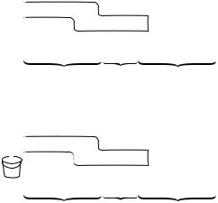
Refer to Figure 4-5. Charge is stored on the parasitic gate capacitance of a MOSFET transistor so that only one transistor is required per bit of storage. The process of reading or sensing the data is destructive in the sense that the charge representing the data is lost when it is sensed. The DRAM capacitor must be refreshed whenever it is read, and also periodically to restore the charge that leaks away. Each row in a DRAM has a sense amplifier and recharge circuitry designed to read and restore the data on an entire row at once. In order to refresh the DRAM data, a special abbreviated read cycle must be performed for each row of the memory. Because of the high density of data storage in DRAMs such as a 4 megabit device, the memory must have 22 address bits to select the location to be read or written. Rather than using 22 individual pins to specify the location, 11 wires are used and the address is latched by the DRAM in two parts: the row address and the column address. This is referred to as a multiplexed address Two control signals, row address strobe (RAS) and
101CHAPTER FOUR
Memory Technologies and Interfacing
column address strobe (CAS, are used to multiplex the two 11-bit halves of the address into the DRAM. To simplify the refresh process, only the row address is used in a refresh cycle. Doing this takes advan tage of the fact that there is one sense and refresh circuit for each bit in a row. The refresh row address is sequenced through all possible addresses before the capacitors can discharge.
One DRAM Bit Cell
|
|
|
|
|
|
|
|
|
|
|
|
|
|
|
|
|
|
|
|
|
|
|
|
|
|
|
|
|
|
|
|
|
|
|
|
|
|
|
|
|
|
|
|
|
|
|
|
|
|
|
|
|
|
|
|
|
|
|
|
|
|
|
|
|
|
|
Gate |
|
|
SiO2 |
|||||
|
|
|
|
|
|
|
|
|
|
|
|
|
|
|||||
|
|
|
|
|
|
|
|
|
|
|
|
|
|
|
|
|
|
|
|
|
|
|
|
|
|
|
|
|
|
|
|
|
|
|
|
|
|
|
|
|
|
|
Semiconductor. |
|
|
|
|
|
|
|
Semiconductor. |
|
|
|
||
|
|
|
|
|
|
|
|
|
|
|
|
|
|
|
||||
|
|
|
|
|
|
|
|
|
|
|
|
|
|
|
||||
|
|
|
|
|
|
|
|
|
|
|
|
|
|
|
|
|
|
|
|
|
|
|
|
|
|
|
|
|
|
|
|
|
|
|
|
|
|
|
|
|
|
|
Source |
|
Channel |
Drain |
||||||||||
|
|
|
|
|
|
|
|
ON or OFF |
|
|
|
|
|
|||||
|
|
|
|
|
|
|
|
depending on |
|
|
|
|
|
|||||
|
|
|
|
|
|
|
|
gate voltage |
|
|
|
|
|
|||||
|
|
|
|
|
|
|
|
|
Charge on gate leaks off slowly, |
|||||||||
|
|
|
|
|
|
|
|
|
||||||||||
|
|
|
|
|
|
|
|
|
and must be “refreshed” periodically |
|||||||||
|
|
|
|
|
|
|
|
|
|
|
|
|
|
|
|
|
|
|
|
|
|
|
|
|
|
|
|
|
|
|
|
|
|
|
|
|
|
|
|
|
|
|
|
|
|
|
|
Gate |
SiO2 |
|||||||
|
|
|
|
|
|
|
|
|
|
|||||||||
|
|
|
|
|
|
|
|
|
|
|
|
|
|
|||||
|
|
|
|
|
|
|
|
|
|
|
|
|
|
|
|
|||
Bit |
|
|
|
Semiconductor. |
|
|
|
|
|
|
|
Semiconductor. |
|
|
||||
|
|
|
|
|
|
|
|
|
||||||||||
|
|
|
|
|
|
|
|
|
|
|
|
|
|
|
|
|
||
|
|
|
|
|
|
|
|
|
|
|
|
|
|
|
|
|
||
Bucket |
|
|
|
Source |
|
Channel |
Drain |
|||||||||||
|
|
|
|
|
|
|||||||||||||
|
|
|
|
|
|
|
|
|
ON |
|
|
|
|
|
||||
Read-Only Memory
Figure 4-5: Dynamic RAM bit storage mechanism.
Read-only memory (ROM) is a class of storage that cannot be erased or modi fied by the processor. Typical embedded systems may make use of one or more of the following types of ROM: mask ROM PROM, EPROM EEPROM or flash EPROM.
Mask ROM is memory that has been programmed at the time it is manufactured and can never be changed. The data patterns are defined by the photographic masks used to define the circuits on a chip when it is being fabricated. Mask ROMs are used when the programs or data do not need to be changed, when the production quantities are large, and the cost must be as low as possible. This is the oldest form of ROM and is still used in high volume applications because of its very low manufacturing cost. The program must be permanently defined in advance by including it as part of the master artwork film or “masks” used to fabricate the chips. It is also the least flexible to change, as a program change necessitates building and packaging new chips, which can take from weeks to months to accomplish.
PROM is user-programmable ROM, which is often used as a generic term for memories that can be programmed one or more times by the user using a special device called a PROM programmer or PROM burner. This was the first “field programmable” memory, meaning that it can be loaded with data by the
103CHAPTER FOUR
Memory Technologies and Interfacing
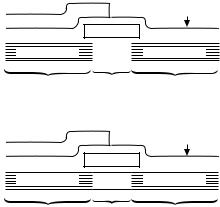
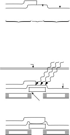
current flow across the insulating region for up to 50 milliseconds, and some of the charge is stranded on the floating gate. Figure 4-7 illustrates the program and read operations of a typical EPROM.
|
Reading a Bit |
|
Charged |
Insulating |
|||||||||||
|
|
Gate |
|||||||||||||
|
|
|
|
|
|
|
|
|
|
|
|
|
Material |
||
|
|
|
|
|
|
|
|
|
|
|
|
|
|||
|
|
|
|
|
|
|
|
|
|
|
|
|
|
||
|
|
|
|
|
|
|
|
|
|
|
|
|
|
|
|
|
|
Metal |
|
|
|
|
|
|
|
|
|
|
|
|
|
|
|
|
|
|
|
|
|
Metal Gate |
|
|
SiO2 |
||||
|
|
|
|
|
|
|
|||||||||
|
|
|
|
|
|
|
|
|
|
|
|
|
|||
|
|
|
|
|
|
|
|
|
|
|
|
|
|||
|
|
|
|
|
|
|
|
|
|
|
|
|
|
|
|
|
|
|
Semiconductor. |
|
|
|
|
|
|
|
|
Semiconductor. |
|
||
|
|
|
|
|
|
||||||||||
|
|
|
|
|
|
|
|
|
|
|
|
|
|
|
|
|
|
|
|
|
|
|
|
|
|
|
|
|
|
|
|
Source Channel Drain