

169CHAPTER EIGHT
Basic I/O Interfaces
device’s inputs are driven by a separately powered device. When power is applied to the previously unpowered device, having the inputs at a higher level than the supply voltage can cause latch-up. By using a resistor in series with the input, as shown in the previous figure, it is possible to limit the current in these conditions to a level which will not cause latch-up to occur.
The 80C32 parameters are different than other members of the 8051 family. The Atmel 89C2051, a low cost 20-pin version, has greater output drive capability than the 80C32. Depending upon which port is used and how it is configured, the output capabilities can also vary, even on the same device.
Processors other than the 8051 family of devices frequently have different characteristics, including: standard tri-state outputs with higher drive capacity and data direction control registers, and much higher output source and sink currents. For example, the Microchip PIC family of processors has devices that are capable of sinking and sourcing up to 25 milliamperes per pin. Note that the price for the higher drive capability is the requirement to write to the data direction register for bi-directional I/O functions, and the potential for bus contention problems. Higher output drive on any microcontroller can be accomplished using external power control devices, designed for driving motors, solenoids, valves, and other larger loads. Some of these devices have additional features, such as current limiting, over temperature shutdown, and so forth. Some also have limited logic built in, and are often referred to as “smart power” devices.
There are several common types of I/O device which can be directly connected to the processor, including simple switches, keypads, LEDs, and LCDs. Input devices can be divided into three categories: simple switches, multiplexed keyboards, and intelligent keyboards as used on the desktop PC. The displays can also be divided into three groups: simple on/off indicators, multiplexed LED or LCD displays, and intelligent display modules. People can also be classified into three groups: those who divide things into groups, those who do not, and those who have no opinion.
Simple Input/Output Devices
The switch is probably the simplest of all input devices, and one of the most useful. Hardware interfacing is quite simple, and for CPUs that have internal pull-ups like the 8051, all that need be done is connect the switch between
170EMBEDDED CONTROLLER
Hardware Design
the pin and ground. As can be seen from Figure 8-7, the input will be a logic one when the switch is open, and logic zero when the switch is closed. Unfortunately switch contacts bounce when they are closed and sometimes when they are broken. This causes
the output to oscillate briefly between |
+V Internal CPU |
+V |
|
one and zero until the contacts stop |
Resistor |
|
|
|
|
||
Sources |
|
|
|
bouncing, usually after several milli- |
Current |
|
|
seconds or more. As a result, the |
|
|
|
|
|
|
|
“1” |
|
|
|
|
|
|
|
|
“0” |
|
|
|
|
|
|
|
|
|
|
|
|
|
|
|
|||
program reading the switch state must |
|
|
|
|
|
|
Switch |
|
|
|
|
|
|
|
|
Output |
|
|
|
|
|
|
|
|
|
|
|
|
|
|
|
||||
|
|
|
|
|
|
|
|
|
|
|
|
|
|
|
Sinks |
||
“de-bounce” the switch operation, |
|
|
|
|
|
|
|
OFF |
Switch |
|
Current |
||||||
meaning that the switch transitions |
|
|
|
|
|
|
(open) |
ON |
|
|
|
|
|||||
|
|
|
|
|
|
|
|
|
|||||||||
|
|
|
|
|
|
|
|
(shorted) |
|
|
|
|
|||||
must be ignored for some time after |
|
|
|
|
|
|
|
|
|
|
|
|
|
|
|
|
|
the first transition between off and on. |
|
|
|
|
|
|
|
|
|
|
|
|
|
|
|
|
|
|
|
|
|
|
|
|
|
|
|
|
|
|
|
|
|
|
|
|
|
|
|
|
|
|
|
|
|
|
|
|
|
|
|
|
|
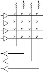
Matrix Keyboard Input
The next step up in input complexity is the matrix keypad or keyboard. These switch arrays are usually organized into a number of rows and columns, like the 4-by-3 array of 12 buttons on a telephone. These matrix-connected devices can be multiplexed to reduce the number of I/O lines required to sense the keys. If a 4-row-by-4-column keypad were implemented using separate inputs, one per switch, a total of 16 input pins would be required. Since I/O pins are almost always at a premium, this is not the best approach.
By arranging the switch contacts to short the row and column lines corresponding to their position in the matrix, the number of lines can be reduced. By selecting one column at a time and looking for activity on any of the row inputs, the program can determine which key has been depressed. One row output can be driven low at a time, and the column input bits are read to see if any of them are low. A low column input indicates that the switch belonging to the corresponding row and column is closed. Multiplexing allows the rows and columns to be scanned for activity under software control. In the case of sixteen keys, only four columns and four rows would be required, or a total of eight I/O pins, compared to 16 for the simple one input per switch approach. For the processors like the 8051 with built-in pull-ups, the only thing that is required is the key switch matrix. A key switch matrix like this can be implemented very inexpensively by using a standard matrix keypad, or by attaching steel switch domes to a PC board with row and column contacts, encapsulated
171 CHAPTER EIGHT
172EMBEDDED CONTROLLER
Hardware Design
many other types of displays, such as most LCDs. In each case, the flicker of the display is normally not apparent to the observer. You can see the strobelike effect by waving your fingers quickly in front of a multiplexed display.
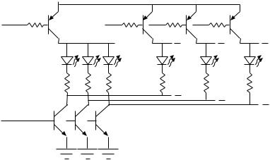
An array of LEDs or seven segment numeric LED displays can be illuminated this way, using many fewer I/O pins than would be required by using one pin per LED, as shown in Figure 8-9.
+5 V
Digit (Column)
Drivers
LEDs
Row (Segment)
Drivers
Figure 8-9: Multiplexed LED display.
The display is scanned, or refreshed, by activating the column, and then the row bits that correspond to the LEDs in that column which should be lit. The display is left on for a short period, then switched to the next column and row, and so on. As long as the display is refreshed frequently enough, there is no visible flicker.
Another type of display is the LCD. The simplest of these is just a glass panel with extremely thin metalized connections to the segments. These are rather complex to drive directly from most microcontrollers, but there are two ways that they can be connected without much effort. The simplest, but more expensive approach, is to use an intelligent LCD module complete with the drive electronics. Most of these devices use a standard controller, and can be driven using either a 4-bit bus or an 8-bit bus. Serial input devices are also available, which can be driven directly from a standard RS-232 serial port. They are available in text-only display versions, ranging in size from one row of 16