

10EMBEDDED CONTROLLER
Hardware Design
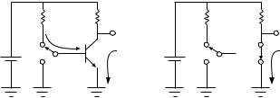
of current flows in the control |
|
|
|
|
|
Collector |
|
|
|
|
|
|
|
circuit (the transistor base- |
|
|
|
|
|
P |
|
|
|
|
|
|
|
emitter circuit) to turn the tran- |
Base |
|
|
|
|
|
|
|
|
|
|||
|
|
N |
|
|
|
|
|
|
|
||||
|
|
|
|
|
|
|
|
|
|||||
sistor on. This control current is |
|
|
|
|
|
P |
|
|
|
|
|
|
|
|
|
|
|
|
|
|
|
|
|
|
|
||
|
|
|
|
|
Emitter |
|
|
|
|
Current |
|
||
amplified (multiplied by the gain |
|
|
|
|
|
|
|
|
|
|
|||
|
|
|
|
|
|
|
|
|
|
Flow |
|
||
or beta of the transistor) and |
|
|
|
|
|
“Source” |
|
|
|
|
|
||
Current |
|
Control |
|
|
|
||||||||
allows a larger current to flow in |
|
|
|
|
|
||||||||
|
|
|
|
|
|||||||||
Flow |
|
|
|
|
|
||||||||
|
|
|
|
|
|
|
|
|
|||||
the output circuit (the collector- |
|
|
|
|
|
|
|
|
|
|
|
|
|
|
|
|
|
|
|
|
|
|
|
|
|
|
|
emitter circuit). Once again, the |
|
|
|
|
|
“Sink” |
|
|
|
|
|
|
|
device is not perfect because of |
|
|
|
|
|
|
|
|
|
|
|
|
|
Figure 1-7: Operation of a bipolar PNP transistor. |
|||||||||||||
the resistance, current, gain, and
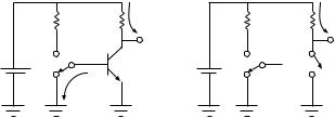
leakage limitations of real transistors. Bipolar transistors come in two polarities, NPN and PNP, with the difference being the direction in which current flows for normal operation. A
bipolar PNP transistor is shown |
|
Collector |
|
|
|
N |
|
|
|
and modeled in Figure 1-7. |
|
|
|
|
Base |
P |
|
|
|
|
|
N |
|
|
For most of the illustrative circuit |
|
Emitter |
Current |
|
examples in this book, we will be |
|
|
|
|
|
“Sink” |
Flow |
|
|
using NPN transistors, as shown |
Current |
|
||
|
|
|
||
|
|
|
||
|
|
|
|
|
in Figure 1-8. |
Flow |
|
|
|
Control |
|
“Source” |
Mechanical Switches
Figure 1-8: Operation of a bipolar NPN transistor.
Mechanical switches are useful for direct input to digital circuits. One of the more convenient versions is a bank of rocker switches packaged into a module that can fit into the same location as a standard chip. The dual in-line package, or DIP, switch is one of the easiest ways to add multiple switches to a microcontroller design. The mechanical switch has extremely low “on” resistance and high “off” resistance, unlike most semiconductor switches. Figure 1-9 shows a typical DIP switch and the schematic symbol for it.
|
|
N |
|
F |
O |
|
|
|
F |
|
|
O |
|
|
Figure 1-9: 8-position DIP switch and schematic equivalent.
11CHAPTER ONE
Review of Electronics Fundamentals
Transistor Switch ON
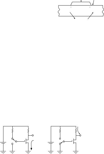
Transistors can be configured to function as switches. As can be seen in Figure 1-10, an NPN transistor operating as a current controlled switch can be used to build a simple inverter. It changes a logic one on its input to a logic zero at its output, and vice versa. In this case, logic one is represented as a positive voltage, and a logic zero is represented by zero volts. The logic one input (positive input voltage) is supplied through a resistor from the power supply voltage to the transistor base terminal, resulting in a small base control current into the base.
Transistor Inverter |
|
|
Transistor Inverter |
|
Input 1 -> Output 0 |
|
|
Equivalent Circuit |
|
Resistor |
|
|
|
|
Sources |
|
|
|
|
Current |
“0” |
|
“1” |
“0” |
“1” |
|
|||
+ |
Output |
+ |
|
Output |
|
Sinks |
|
|
Sinks |
Transistor |
Current |
|
Transistor |
Current |
ON |
|
|
ON |
|
(shorted) |
|
|
(shorted) |
|
Transistor Switch “ON” |
|
|
Equivalent Circuit |
|
Figure 1-10: The transistor inverter; input = 1 and transistor ON. The transistor
ON configuration is at left and the equivalent circuit is at right.
The transistor is used because it has gain allowing a larger output current to flow as controlled by a weaker input. When the transistor is turned on as much as it can be, the collector emitter circuit looks almost like a short circuit, effectively connecting the output to ground or zero volts. This gives a logic zero on the collector output. When the transistor collector is shorted to ground, current flows from the supply through the resistor and into the transistor collector to ground. The transistor is said to sink the resistor current into ground. If there is an external load, such as another inverter or gate, connected to the collector output, the transistor can also sink current from the load. This is also referred to as pulling down the output voltage. The current sinking capacity of the transistor limits the number of devices this inverter can drive.
12EMBEDDED CONTROLLER
Hardware Design
Transistor Switch OFF
When the input is connected to logic zero (ground voltage), no current flows into the base of the transistor, since its base and emitter terminals are at the same voltage. When there is no current flowing in the base, the transistor will not allow current to flow in the collector emitter circuit either. As a result, the circuit behaves as if the transistor was removed from the circuit. The output resistor will source current to any potential load. The output is pulled up to the supply voltage, resulting in a logic one at the output. Once again, there is a limit to the resistor’s ability to source current, resulting in a limit to the number of loads that can be attached to this circuit’s output. Notice these two limits are defined by the ability of the transistor to pull down the output, and the resistor’s ability to pull up the output become the main limits to its ability to drive other devices. Gates can be constructed by adding diodes or transistors to the inverter circuit in Figure 1-11.
Transistor Inverter |
|
Transistor Inverter |
|
Input 0 -> Output 1 |
|
Equivalent Circuit |
|
|
Resistor |
|
Resistor |
|
Sources |
|
Sources |
|
Current |
|
Current |
“0” |
“1” |
“0” |
“1” |
+ |
Transistor |
+ |
Transistor |
Input |
OFF |
|
OFF |
(open) |
|
(open) |
|
Sinks |
|
||
|
|
|
|
Current |
|
|
|
Transistor Switch “OFF” |
Equivalent Circuit |
|
|
Figure 1-11: The transistor inverter; input = 0 and transistor OFF.
The transistor OFF configuration is at left and the equivalent circuit is at right.
The FET as a Logic Switch
Most of the logic devices used in highly integrated circuits do not use bipolar transistors. Instead, they use field effect transistors. FETs perform a similar function
to the bipolar transistors discussed earlier, but they are voltage |
|
Drain |
||||
|
||||||
controlled. While the current flowing in the base |
|
|
|
|
|
|
controls bipolar transistors, the voltage between the |
|
Gate |
|
|
|
|
|
|
|
|
|
||
|
|
|
|
|
||
gate and source controls field effect transistors. The |
|
|
|
|
|
|
|
|
|
|
|
|
|
gate voltage of a field effect transistor controls the |
|
|
|
|
|
|
|
|
|
|
|
|
|
current flowing in the drain-source circuit. The |
Figure 1-12: Field |
|
|
|||
symbol for the FET shows the gate to be insulated |
effect transistor (FET) |
|
Source |
|||
schematic diagram. |
|
|||||
|
|
|
||||
from the source-drain circuit, as shown in Figure 1-12.
13CHAPTER ONE
Review of Electronics Fundamentals
This type of FET is referred to as a MOSFET (metal oxide semiconductor FET), since the insulating material is silicon dioxide (SiO2), commonly known as glass (for early devices, the gate was made
of metal). Like bipolar NPN and PNP |
|
|
Conductor |
SiO2 |
||
|
|
Insulator |
||||
|
|
|
|
|||
transistors with opposite polarity, FETs |
|
|
Gate |
|
|
|
come in N- and P- channel varieties. |
|
|
|
|
|
|
|
Drain |
Channel |
Source |
|
||
The N- and P- channels refer to the |
|
|
||||
|
|
|
|
|
|
|
|
|
|
|
|
|
|
polarity of the source drain element |
|
|
Conductors |
|
|
|
of the device. A cross-section view |
|
|
|
|
||
|
|
|
|
|
|
|
of a FET is shown in Figure 1-13. |
Figure 1-13: Field effect transistor cross-section. |
|||||
NMOS Logic
The conductive state of the FET’s channel is what allows or prevents current from flowing in the device. For a typical logic N-channel MOSFET, the channel becomes conductive when the gate has a positive voltage with respect to the source, allowing current to flow between the drain and source terminals. When the gate is at the same voltage as the source, no current flows. The design of MOS logic circuits can be almost exactly equivalent to the bipolar inverter we saw earlier, substituting an N-channel MOSFET for the bipolar NPN transistor. In fact, the most of the early microcontroller integrated circuits were manufactured using variations of this method, and are referred to as NMOS logic. As can be seen from Figure 1-14, the NMOS FET circuit behaves in an equivalent way to the NPN transistor inverter. When the gate (control input) of the NMOS FET is at a positive voltage, the FET is ON, effectively shorting the source and drain pins. When the gate is at 0 volts, the FET is OFF, opening the circuit between the source and drain. Older NMOS logic ICs use this type of circuit. The original 8051 microcontroller was an NMOS processor.
NMOS FET Inverter |
|
NMOS FET Inverter |
|
Input 1 -> Output 0 |
|
Input 1 -> Output 0 |
|
|
|
|
Resistor |
|
|
|
Sources |
|
|
|
Current |
“1” |
“0” |
“1” |
“0” |
+ |
Output |
+ |
NMOS FET |
|
Sinks |
|
|
NMOS FET |
Current |
|
OFF |
ON |
|
|
(open) |
(shorted) |
|
|
|
Figure 1-14: NMOS inverter circuit.