

ARM cross development with Eclipse, version 2 (J.P. Lynch, 2005)
.pdfThis part of the crt.s file sets up the interrupt vectors.
Note that all of the code and data that follows goes into the .text section. It is also in ARM 32-bit code (not Thumb).
One label is made global, _startup. This will be available to other modules in the project and will also appear in the map.
The GNU assembler doesn’t require you .extern anything. If a symbol is not defined in the assembler file, it is automatically assumed to be external.
The vector table is 32 bytes long and is required to be placed at address 0x000000.
You will see later in this tutorial that the interrupt service routines referenced in the
Vector Table are just endless-loop stubs in the main.c function and the interrupts are turned off.
The NOP instruction at address 14 is an empty spot to hold the checksum. Page 179 of the Philips LPC2106 manual states:
The reserved ARM interrupt vector location (0x0000 0014) should contain the 2’s complement of the check-sum of the remaining interrupt vectors. This causes the checksum of all of the vectors together to be 0.
Before you fall on your sword, you’ll be happy to know that the Philips Flash Loader will calculate that checksum and insert it for you. That’s why we show it as a NOP.
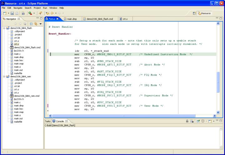
This part of the crt.s file sets up the various interrupt modes and stacks.
The label Reset_Handler is the beginning of the code. Recall that the first interrupt vector at address 0x000000 loads the PC with the contents of the address Reset_Addr, which contains the address of the startup code at the label Reset_Handler. This trick, used in the entire vector table, loads a 32-bit constant into the PC and thus can jump to any address in memory space.
_vectors: |
ldr PC, Reset_Addr |
|
: |
Reset_Addr: |
.word Reset_Handler |
Whenever the LPC2106 is reset, the instruction at 0x000000 is executed first; it jumps to Reset_Handler. From that point, we are off and running!
The first part of the startup code above sets up the stacks and the mode bits.
The symbol _stack_end will be defined in the linker command script file demo2106.cmd. Here is how it will be defined. Knowing that the Philips ISP Flash
Loader will use the very top 288 bytes of RAM for its internal stack and variables, we’ll start our application stacks at 0x4000FEE0.
(Note: 0x40010000 – 0x120 = 0x4000FEE0)
/* define a global symbol _stack_end, placed at the very end of RAM (minus 4 bytes) */ stack_end = 0x4000FEE0 – 4;
Working that out with the Windows calculator, the _stack_end is placed at 4000FEDC.
The code snippet that sets up the stacks and modes is a bit complex, so let’s explain it a bit.
First we load R0 with the address of the end of the stack, as described above.
ldr r0, =_stack_end
Now we put the ARM into Undefined Instruction mode by setting the MODE_UND bit in the Current Program Status Register (CPSR). The four modes undefined, irq, abort and svc all have their own private copies of R13 (sp) and r14 (link return). The FIQ mode has private copies of registers R8 – R14. Thus, by writing R0 into the stack pointer sp
(R13), it will use 0x4000FEDC as the initial stack pointer if we ever have processing of an undefined instruction. By subtracting the undefined stack size (4 bytes) from R0, we’re limiting the stack for UND mode to just 4 bytes.
msr |
CPSR_c, #MODE_UND|I_BIT|F_BIT |
/* This puts the CPU in undefined mode */ |
mov |
sp, r0 |
/* stack pointer for UND mode is 0x40000FEDC */ |
sub |
r0, r0, #UND_STACK_SIZE |
/* Register R0 is now 0x4000FED8 */ |
Now we put the ARM into Abort mode by setting the MODE_ABT bit in the CPSR. As mentioned above, abort mode has its own private copies of R13 and R14. We now set the abort mode stack pointer to 0x4000FED8. Again by subtracting the abort stack size from R0, we’re limiting the stack for ABT mode to just 4 bytes.
msr |
CPSR_c, #MODE_ABT|I_BIT|F_BIT |
/* this puts CPU in Abort mode */ |
mov |
sp, r0 |
/* stack pointer for ABT mode is 0x4000FED8 */ |
sub |
r0, r0, #ABT_STACK_SIZE |
/* Register R0 is now 0x4000FED4 */ |
Now we put the ARM into FIQ (fast interrupt) mode by setting the MODE_FIQ bit in the CPSR. As mentioned above, FIQ mode has its own private copies of R14 through R8. We now set the abort mode stack pointer to 0x4000FED4. Again by subtracting the abort stack size from R0, we’re limiting the stack for FIQ mode to just 4 bytes. We’re not planning to support FIQ interrupts in this example.
msr |
CPSR_c, #MODE_FIQ|I_BIT|F_BIT |
/* this puts CPU in FIQ mode */ |
mov |
sp, r0 |
/* stack pointer for FIQ mode is 0x4000FED4 |
sub |
r0, r0, #FIQ_STACK_SIZE |
/* Register R0 is now 0x4000FED0 */ |
Now we put the ARM into IRQ (normal interrupt) mode by setting the MODE_IRQ bit in the CPSR. As mentioned above, IRQ mode has its own private copies of R13 and R14. We now set the IRQ mode stack pointer to 0x4000FDE0. Again by subtracting the IRQ stack size from R0, we’re limiting the stack for IRQ mode to just 4 bytes. We’re not planning to support IRQ interrupts in this example.
msr |
CPSR_c, #MODE_IRQ|I_BIT|F_BIT |
/* this puts the CPU in IRQ mode */ |
mov |
sp, r0 |
/* stack pointer for IRQ mode is 0x4000FED0 */ |
sub |
r0, r0, #IRQ_STACK_SIZE |
/* R0 is now 0x4000FECC */ |

Now we put the ARM into SVC (Supervisor) mode by setting the MODE_SVC bit in the CPSR. As mentioned above, SVC mode has its own private copies of R13 and R14. We now set the supervisor mode stack pointer to 0x4000FDDC. Again by subtracting the SVC stack size(4 bytes) from R0, we’re sizing the stack for SVC mode to 4 bytes.
msr |
CPSR_c, #MODE_SVC|I_BIT|F_BIT |
/* This puts the CPU in SVC mode */ |
mov |
sp, r0 |
/* stack pointer for SVC mode is 0x4000FECC */ |
sub |
r0, r0, #SVC_STACK_SIZE |
/* R0 is now 0x4000FEC8 */ |
The ARM “User” mode and the ARM “System” mode share the same registers and stack. For this very simple example, we’ll run the application in “User” mode. Setting up the stack for User mode also sets up the stack for System mode.
Now we put the ARM into USR (user) mode by setting the MODE_USR bit in the CPSR. We now set the USR mode stack pointer to 0x4000FEC8.
msr |
CPSR_c, #MODE_USR|I_BIT|F_BIT |
/* User Mode */ |
mov |
sp, r0 |
|
To summarize the above operations, let’s draw a diagram of the stacks we just created.
RAM STACK USAGE
Philips ISP Flash Loader
Stack and variables
(288. bytes)
Undefined mode stack ( 4 bytes )
Abort mode stack |
( 4 bytes ) |
|
|
FIQ mode stack |
( 4 bytes ) |
|
|
IRQ mode stack |
( 4 bytes ) |
|
|
SVC mode |
( 4 bytes ) |
RAM
USR mode / SYS mode stack
Stack grows downward
( until it collides with
0x40010000
0x4000FFFF last address in internal
0x4000FEE0 |
bottom of Philips ISP |
0x4000FEDC |
UND stack pointer |
0x4000FED8 |
ABT stack pointer |
0x4000FED4 |
FIQ stack pointer |
0x4000FED0 |
IRQ stack pointer |
0x4000FECC |
SVC stack pointer |
0x4000FEC8 |
USR / SYS stack |
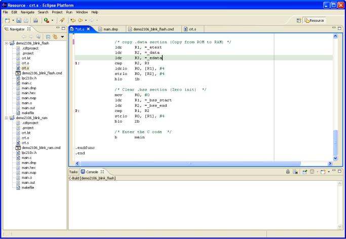
The next part of the startup file crt.s to investigate is the setup of the .data and .bss sections, as shown below.
The .data section contains all the initialized static and global variables. The GNU linker will create a exact copy of the variables in flash with the correct initial values loaded. The onus is on the programmer to copy this initialized flash copy of the data to RAM.
The location of the start of the .data section in flash is defined by symbol _etext (defined in the linker command script demo2106.cmd). Likewise, the location of the start and end of the .data section in destination RAM is given by the symbols _data and
_edata. Both of these symbols are defined in the linker command script.
The .bss section contains all the uninitialized static and global variables. All we have to do here is clear this area. Likewise, the location of the start and end of the .bss section in destination RAM is given by the symbols _bss_start and _bss_end. Both of these symbols are defined in the linker command script.
Two simple assembly language loops load the .data section in RAM with the initializers in flash and clear out the .bss section in RAM.
The GNU linker specifies two addresses for sections, the Virtual Memory Address (VMA) and the Load memory Address (LMA). The VMA is the final destination for the section; for the .data section, this is the RAM address where it will reside. The LMA is
where it will be loaded in Flash memory, the exact copy with the initial values. The GNU Linker will sort this out for us.
14 Description of the Main Program main.c
Now let’s look at the main program.
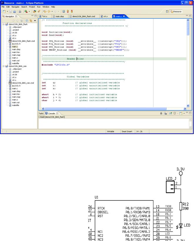
The main program starts out with a few function prototypes. Note that the interrupt routines mentioned in the crt.s assembler program reside in the main() program. We’ve used the GNU C compiler syntax that identifies the interrupt routines and makes sure that the compiler will save and restore registers, etc. whenever the interrupt is asserted.
I’ve also included a few do-nothing variables, both initialized and uninitialized, to illustrate that the compiler will put the initialized variables into the .data section and the uninitialized ones into the .bss section.
We’re going to try to toggle a single I/O bit, specifically P0.7 which is the Olimex red LED.

By the way, with this hardware arrangement:
P0.7 = 1 // turn off LED
P0.7 = 0 // turn on LED
The Philips LPC2106 has 32 I/O pins, labeled P0.0 through P0.31. Most of these pins have two or three possible uses. For example, pin P0.7 has three possible uses; digital
I/O port, SPI Slave Select and PWM output 2. Normally, you select which function to use with the Pin Connect Block. The Pin Connect Block is composed of two 32-bit registers, PINSEL0 and PINSEL1. Each Pin Select register has two bits for each I/O pin, allowing at least three functions for each pin to be specified.
For example, pin P0.7 is controlled by PINSEL0, bits 14 – 15. The following specification would select PWM2 output.
PINSEL0 = 0x00008000; // set PINSEL0 bits 14 – 15 to 01
Fortunately, the Pin Connect Block resets to zero, meaning that all port pins are General-Purpose I/O bits. So we don’t have to set the Pin Select registers in this example.
We do have to set the I/O Direction for port P0.7, this can be done in this way.
IODIR |= 0x00000080; |
// set IO Direction register, P0.7 as output |
|
// 1 = output, 0 = input |
The ARM I/O ports are manipulated by register IOSET and register IOCLR. You never directly write to the I/O Port! You set a bit in the IOSET register to set the port bit and you set a bit in the IOCLR register to clear the port bit. This little nuance will trip up novice and experienced programmers alike. Alert readers will ask; “What if both bits are set in IOSET and IOCLR?” The answer is “Last one wins.” The last IOSET or IOCLR instruction will prevail.
To turn the LED P0.7 off, we can write:
IOSET = 0x00000080; |
// turn P0.7 (red LED) off |
Likewise, to turn the LED P0.7 on, we can write:
IOCLR = 0x00000080; // turn P0.7 (red LED) on
As you can see, it’s fairly simple to manipulate I/O bits on the ARM processor.
To blink the LED, a simple FOREVER loop will do the job. I selected the loop counter values to get a one half second blink on – off time.
// endless loop to toggle the red LED P0.7 while (1) {
for (j = 0; j < 5000000; j++ ); |
// wait 500 msec |
IOSET = 0x00000080; |
// red led off |
for (j = 0; j < 5000000; j++ ); |
// wait 500 msec |
IOCLR = 0x00000080; |
// red led on |
} |
|
This scheme is very inefficient in that it hog-ties the CPU while the wait loops are counting up.
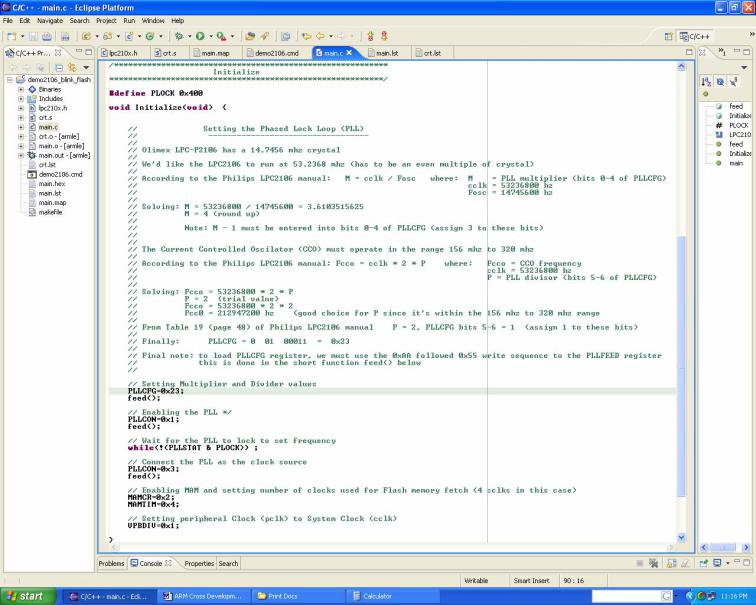
The Initialize(); function requires some explanation.
We have to set up the Phased Lock Loop (PLL) and that takes some math.
Olimex LPC-P2106 board has a 14.7456 Mhz crystal
We'd like the LPC2106 to run at 53.2368 Mhz (has to be an even multiple of crystal, in this case 3x)
According to the Philips LPC2106 manual: M = cclk / Fosc |
where: M = PLL multiplier (bits 0-4 of |
PLLCFG) |
cclk = 53236800 hz |
|
|
|
Fosc = 14745600 hz |
Solving:M = 53236800 / 14745600 = 3.6103515625 |
|
M = 4 (round up) |
|
Note: M - 1 must be entered into bits 0-4 of PLLCFG (assign 3 to these bits)
The Current Controlled Oscillator (CCO) must operate in the range 156 Mhz to 320 Mhz
According to the Philips LPC2106 manual: |
Fcco = cclk * 2 * P where: |
Fcco = CCO frequency |
||
|
|
|
cclk = 53236800 hz |
|
|
|
|
P = PLL divisor (bits 5-6 of PLLCFG) |
|
Solving: |
Fcco = 53236800 * 2 |
* P |
|
|
|
P = 2 (trial value) |
|
|
|
|
Fcco = 53236800 * 2 |
* 2 |
|
|
Fcc0 = 212947200 hz (good choice for P since it's within the 156 mhz to 320 mhz range From Table 19 (page 48) of Philips LPC2106 manual P = 2, PLLCFG bits 5-6 = 1 (assign 1 to these bits)
Finally: PLLCFG = 0 01 00011 = 0x23
Final note: to load PLLCFG register, we must use the 0xAA followed 0x55 write sequence to the PLLFEED register
this is done in the short function feed() below
With the math completed, we can set the Phase Locked Loop Configuration Register
(PLLCFG)
// Setting Multiplier and Divider values PLLCFG = 0x23;
feed();
To set values into the PLLCON and PLLCFG registers, you have to write a twobyte sequence to the PLLFEED register:
PLLFEED = 0xAA;
PLLFEED = 0x55;
This sequence is coded in a short function feed();
The net effect of the above setup is to run the ARM CPU at 53.2 Mhz.
Next we fully enable the Memory Accelerator module and set the Flash memory to run at ¼ the clock speed. Now you see why some people prefer to execute out of RAM where it’s much faster.
//Enabling MAM and setting number of clocks used for Flash memory fetch
//(4 cclks in this case)
MAMCR=0x2;
MAMTIM=0x4;
The clock speed of the peripherals is also run at 53.2 Mhz which is the full clock speed.
// Setting peripheral Clock (pclk) to System Clock (cclk) VPBDIV=0x1;