

IKP40N65H5
.pdfIKW40N65H5, IKP40N65H5
High speed switching series fifth generation
|
1.6 |
|
|
|
|
|
|
|
|
|
0.8 |
|
|
|
|
|
|
|
|
Eoff |
|
|
|
|
|
|
|
|
|
Eoff |
|
|
|
|
|
|
|
Eon |
|
|
|
|
|
|
|
|
|
Eon |
|
|
|
|
|
|
1.4 |
Ets |
|
|
|
|
|
|
|
|
0.7 |
Ets |
|
|
|
|
|
E[mJ]LOSSESENERGYSWITCHING, |
1.2 |
|
|
|
|
|
|
|
|
E[mJ]LOSSESENERGYSWITCHING, |
0.6 |
|
|
|
|
|
|
1.0 |
|
|
|
|
|
|
|
|
0.5 |
|
|
|
|
|
|
||
0.8 |
|
|
|
|
|
|
|
|
0.4 |
|
|
|
|
|
|
||
0.6 |
|
|
|
|
|
|
|
|
0.3 |
|
|
|
|
|
|
||
0.4 |
|
|
|
|
|
|
|
|
0.2 |
|
|
|
|
|
|
||
|
|
|
|
|
|
|
|
|
|
|
|
|
|
|
|
||
|
0.2 |
|
|
|
|
|
|
|
|
|
0.1 |
|
|
|
|
|
|
|
0.0 |
|
|
|
|
|
|
|
|
|
0.0 |
|
|
|
|
|
|
|
5 |
15 |
25 |
35 |
45 |
55 |
65 |
75 |
85 |
|
25 |
50 |
75 |
100 |
125 |
150 |
175 |
|
|
|
rG, GATE RESISTOR [Ω] |
|
|
|
|
Tvj, JUNCTION TEMPERATURE [°C] |
|
||||||||
|
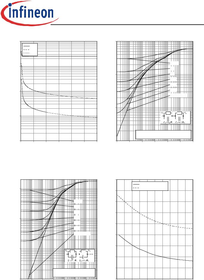
Figure 13. Typical switching energy losses as a |
|
|
Figure 14. Typical switching energy losses as a |
|
||||||||||||
|
|
function of gate resistor |
|
|
|
|
|
function of junction temperature |
|
||||||||
|
|
(inductive load, Tvj=150°C, VCE=400V, |
|
|
|
(inductive load, VCE=400V, VGE=15/0V, |
|
||||||||||
|
|
VGE=15/0V, IC=20A, Dynamic test circuit in |
|
|
IC=20A, rG=15Ω,Dynamic test circuit in |
|
|||||||||||
|
|
Figure E) |
|
|
|
|
|
|
|
|
Figure E) |
|
|
|
|
|
|
|
1.0 |
|
|
|
|
|
|
|
|
|
16 |
|
|
|
|
|
|
|
|
Eoff |
|
|
|
|
|
|
|
|
|
130V |
|
|
|
|
|
|
0.9 |
Eon |
|
|
|
|
|
|
|
|
|
520V |
|
|
|
|
|
|
Ets |
|
|
|
|
|
|
|
|
14 |
|
|
|
|
|
|
|
|
|
|
|
|
|
|
|
|
|
|
|
|
|
|
|
||
[mJ]LOSSESENERGYSWITCHING, |
0.8 |
|
|
|
|
|
|
|
|
VGEGATE,-[V]VOLTAGEEMITTER |
|
|
|
|
|
|
|
|
|
|
|
|
|
|
|
|
12 |
|
|
|
|
|
|
||
0.7 |
|
|
|
|
|
|
|
|
|
|
|
|
|
|
|
||
0.6 |
|
|
|
|
|
|
|
|
10 |
|
|
|
|
|
|
||
|
|
|
|
|
|
|
|
|
|
|
|
|
|
|
|||
0.5 |
|
|
|
|
|
|
|
|
8 |
|
|
|
|
|
|
||
0.4 |
|
|
|
|
|
|
|
|
6 |
|
|
|
|
|
|
||
|
|
|
|
|
|
|
|
|
|
|
|
|
|
|
|||
0.3 |
|
|
|
|
|
|
|
|
|
|
|
|
|
|
|
||
|
|
|
|
|
|
|
|
|
4 |
|
|
|
|
|
|
||
0.2 |
|
|
|
|
|
|
|
|
|
|
|
|
|
|
|
||
E |
|
|
|
|
|
|
|
|
|
|
|
|
|
|
|
|
|
|
0.1 |
|
|
|
|
|
|
|
|
|
2 |
|
|
|
|
|
|
|
|
|
|
|
|
|
|
|
|
|
|
|
|
|
|
|
|
|
0.0 |
|
|
|
|
|
|
|
|
|
0 |
|
|
|
|
|
|
|
200 |
250 |
|
300 |
350 |
400 |
|
450 |
500 |
|
0 |
20 |
|
40 |
60 |
80 |
100 |
|
|
VCE, COLLECTOR-EMITTER VOLTAGE [V] |
|
|
|
QGE, GATE CHARGE [nC] |
|
|
|||||||||
|
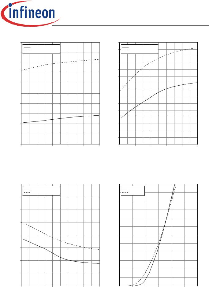
Figure 15. Typical switching energy losses as a |
|
|
Figure 16. Typical gate charge |
|
|
|
||||||||||
|
|
function of collector emitter voltage |
|
|
|
(IC=40A) |
|
|
|
|
|
||||||
|
|
(inductive load, Tvj=150°C, VGE=15/0V, |
|
|
|
|
|
|
|
|
|
||||||
|
|
IC=20A, rG=15Ω,Dynamic test circuit in |
|
|
|
|
|
|
|
|
|
||||||
|
|
Figure E) |
|
|
|
|
|
|
11 |
|
|
|
|
Rev. 1.2, 2013-12-18 |
|||
|
|
|
|
|
|
|
|
|
|
|
|
|
|
||||
IKW40N65H5, IKP40N65H5
High speed switching series fifth generation
|
1E+4 |
|
|
1 |
|
|
|
|
|
|
Ciss |
|
|
|
|
|
|
,CAPACITANCE[pF]C |
|
Coss |
,TRANSIENTTHERMALRESISTANCE[K/W]c) |
|
|
|
|
|
|
Crss |
|
|
|
|
|
||
|
|
|
|
|
|
|
|
|
|
1000 |
|
|
|
|
|
D=0.5 |
|
|
|
|
|
|
|
0.2 |
|
|
|
|
|
|
|
|
|
|
|
|
|
|
|
0.1 |
|
|
0.1 |
|
|
|
|
|
|
|
|
0.05 |
|
|
|
|
|
|
|
|
0.02 |
|
|
100 |
|
|
|
|
|
0.01 |
|
|
|
|
|
|
|
|
single pulse |
|
|
|
|
|
0.01 |
|
|
|
|
|
10 |
|
|
|
|
|
|
|
|
|
|
th(j- |
|
|
|
|
|
|
|
|
Z |
i: |
1 |
2 |
3 |
4 |
|
|
|
|
|||||
|
|
|
|
ri[K/W]: |
0.08245484 |
0.144197 |
0.2151774 |
0.1581708 |
|
|
|
|
τi[s]: |
7.3E-5 |
7.0E-4 |
0.01235548 |
0.08020881 |
1 |
|
|
|
|
|
|
|
|
0.001 |
|
|
|
|
|
|
0 |
5 |
10 |
|
15 |
20 |
25 |
30 |
|
1E-6 |
1E-5 |
1E-4 |
0.001 |
0.01 |
0.1 |
1 |
VCE, COLLECTOR-EMITTER VOLTAGE [V] |
|
|
|
|
tp, PULSE WIDTH [s] |
|
|
||||||||
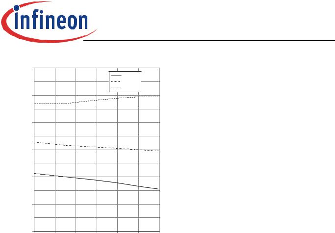
Figure 17. Typical capacitance as a function of |
|
|
Figure 18. IGBT transient thermal resistance |
|
|||||||||||
|
collector-emitter voltage |
|
|
|
|
|
(D=tp/T) |
|
|
|
|
|
|||
|
(VGE=0V, f=1MHz) |
|
|
|
|
|
|
|
|
|
|
|
|
||
|
|
|
|
|
|
|
|
|
130 |
|
|
|
|
|
|
1 |
|
|
|
|
|
|
|
|
|
|
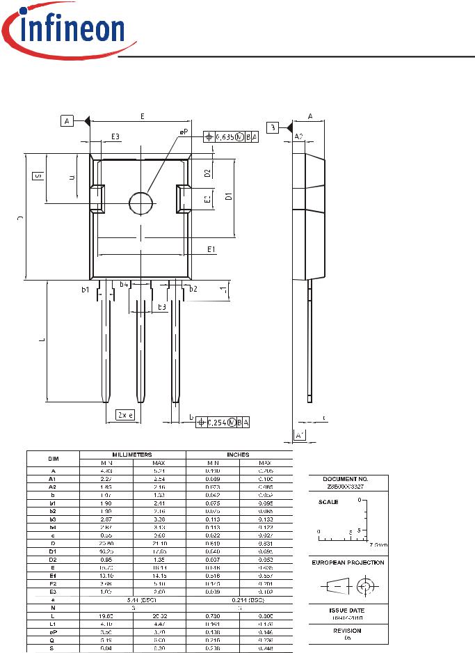
Tj=25°C, IF = 20A |
|
|
||
|
|
|
|
|
|
|
|
120 |
|
Tj=150°C, IF = 20A |
|
|
|||
|
|
|
|
|
|
|
|
|
|
|
|
|
|
|
|
|
|
|
|
|
D=0.5 |
|
|
110 |
|
|
|
|
|
|
|
|
|
|
|
|
0.2 |
|
|
|
|
|
|
|
|
|
|
|
|
|
|
|
0.1 |
|
|
|
100 |
|
|
|
|
|
|
0.1 |
|
|
|
|
0.05 |
|
|
|
|
|
|
|
|
|
|
|
|
|
|
|
0.02 |
|
|
|
90 |
|
|
|
|
|
|
|
|
|
|
|
0.01 |
|
|
|
|
|
|
|
|
|
|
|
|
|
|
|
single pulse |
|
|
80 |
|
|
|
|
|
|
|
0.01 |
|
|
|
|
|
|
|
|
70 |
|
|
|
|
|
|
|
|
|
|
|
|
|
|
|
|
|
|
|
|
|
|
[K/W]RESISTANCETHERMALTRANSIENT,c) |
|
|
|
|
|
|
|
[ns]TIMERECOVERYREVERSE,trr |
60 |
|
|
|
|
|
|
|
|
|
|
|
|
|
|
|
|
|
|
|
|
||
th(j- |
|
|
|
|
|
|
|
|
50 |
|
|
|
|
|
|
Z |
|
|
i: |
1 |
2 |
3 |
|
|
|
|
|
|
|
|
|
|
|
|
|
|
|
|
|
|
|
|
|||||
|
|
|
|
|
|
|
|
|
|
|
|
||||
|
|
|
ri[K/W]: 0.6701584 0.775759 |
0.3540826 |
|
|
|
|
|
|
|
|
|
||
|
|
|
τi[s]: 3.4E-4 |
4.7E-3 |
0.04680901 |
|
|
|
|
|
|
|
|
|
|
0.001 |
|
|
|
|
|
|
|
|
40 |
|
|
|
|
|
|
1E-7 |
1E-6 |
1E-5 |
1E-4 |
0.001 |
0.01 |
0.1 |
1 |
|
500 |
700 |
900 |
|
1100 |
1300 |
1500 |
|
|
tp, PULSE WIDTH [s] |
|
|
|
|
diF/dt, DIODE CURRENT SLOPE [A/µs] |
|
|||||||
Figure 19. Diode transient thermal impedance as a |
|
Figure 20. Typical reverse recovery time as a function |
|||||||||||||
|
function of pulse width |
|
|
|
|
|
of diode current slope |
|
|
||||||
|
(D=tp/T) |
|
|
|
|
|
|
|
(VR=400V) |
|
|
|
|
||
|
|
|
|
|
|
|
|
12 |
|
|
|
|
Rev. 1.2, 2013-12-18 |
||
IKW40N65H5, IKP40N65H5
High speed switching series fifth generation
|
1.2 |
|
|
|
|
|
|
20 |
|
|
|
|
|
|
|
|
Tj=25°C, IF = 20A |
|
|
|
|
19 |
Tj=25°C, IF = 20A |
|
|
|
|||
|
|
Tj=150°C, IF = 20A |
|
|
|
|
Tj=150°C, IF |
= 20A |
|
|
|
|||
|
|
|
|
|
|
|
|
|
|
|||||
Qrr[µC]CHARGERECOVERYREVERSE, |
|
|
|
|
|
|
Irr[A]CURRENTRECOVERYREVERSE, |
18 |
|
|
|
|
|
|
1.0 |
|
|
|
|
|
17 |
|
|
|
|
|
|
||
|
|
|
|
|
|
16 |
|
|
|
|
|
|
||
|
|
|
|
|
|
15 |
|
|
|
|
|
|
||
0.8 |
|
|
|
|
|
14 |
|
|
|
|
|
|
||
|
|
|
|
|
|
13 |
|
|
|
|
|
|
||
|
|
|
|
|
|
12 |
|
|
|
|
|
|
||
0.6 |
|
|
|
|
|
11 |
|
|
|
|
|
|
||
|
|
|
|
|
|
10 |
|
|
|
|
|
|
||
0.4 |
|
|
|
|
|
9 |
|
|
|
|
|
|
||
|
|
|
|
|
8 |
|
|
|
|
|
|
|||
|
|
|
|
|
|
7 |
|
|
|
|
|
|
||
|
|
|
|
|
|
|
|
|
|
|
|
|
|
|
|
|
|
|
|
|
|
|
6 |
|
|
|
|
|
|
|
0.2 |
|
|
|
|
|
|
5 |
|
|
|
|
|
|
|
500 |
700 |
900 |
1100 |
1300 |
1500 |
|
500 |
700 |
|
900 |
1100 |
1300 |
1500 |
|
|
diF/dt, DIODE CURRENT SLOPE [A/µs] |
|
|
|
diF/dt, DIODE CURRENT SLOPE [A/µs] |
|
|||||||
|
Figure 21. Typical reverse recovery charge as a |
|
|
Figure 22. Typical reverse recovery current as a |
|
|||||||||
|
|
function of diode current slope |
|
|
|
function of diode current slope |
|
|||||||
|
|
(VR=400V) |
|
|
|
|
|
|
(VR=400V) |
|
|
|
|
|
|
0 |
|
|
|
|
|
|
60 |
|
|
|
|
|
|
|
|
Tj=25°C, IF = 20A |
|
|
|
|
|
Tj=25°C |
|
|
|
|
|
|
|
|
Tj=150°C, IF = 20A |
|
|
|
|
|
Tj=150°C |
|
|
|
|
||
|
-50 |
|
|
|
|
|
|
50 |
|
|
|
|
|
|
rr/dtoffallofratepeakdiode,Irr[A/µs] |
|
|
|
|
|
|
|
|
|
|
|
|
|
|
-100 |
|
|
|
|
|
IF[A]CURRENTFORWARD, |
|
|
|
|
|
|
|
|
-150 |
|
|
|
|
|
40 |
|
|
|
|
|
|
||
|
|
|
|
|
|
|
|
|
|
|
|
|||
-200 |
|
|
|
|
|
30 |
|
|
|
|
|
|
||
-250 |
|
|
|
|
|
20 |
|
|
|
|
|
|
||
|
|
|
|
|
|
|
|
|
|
|
|
|||
-300 |
|
|
|
|
|
|
|
|
|
|
|
|
||
|
|
|
|
|
|
|
|
|
|
|
|
|
||
dI |
|
|
|
|
|
|
|
10 |
|
|
|
|
|
|
|
-350 |
|
|
|
|
|
|
|
|
|
|
|
|
|
|
|
|
|
|
|
|
|
|
|
|
|
|
|
|
|
-400 |
|
|
|
|
|
|
0 |
|
|
|
|
|
|
|
500 |
700 |
900 |
1100 |
1300 |
1500 |
|
0.0 |
0.5 |
1.0 |
1.5 |
2.0 |
2.5 |
3.0 |
|
|
diF/dt, DIODE CURRENT SLOPE [A/µs] |
|
|
|
VF, FORWARD VOLTAGE [V] |
|
|||||||
|
Figure 23. Typical diode peak rate of fall of reverse |
|
Figure 24. Typical diode forward current as a function |
|||||||||||
|
|
recovery current as a function of diode |
|
|
of forward voltage |
|
|
|
||||||
|
|
current slope |
|
|
|
|
|
|
|
|
|
|
|
|
|
|
(VR=400V) |
|
|
|
|
|
|
|
|
|
|
|
|
|
|
|
|
|
|
13 |
|
|
|
|
Rev. 1.2, 2013-12-18 |
|||
IKW40N65H5, IKP40N65H5
High speed switching series fifth generation
2.0 |
|
|
|
|
|
|
|
|
|
|
|
IF=10A |
|
|
|
|
|
|
IF=20A |
|
|
|
|
|
|
IF=40A |
|
1.8 |
|
|
|
|
|
|
1.6 |
|
|
|
|
|
|
1.4 |
|
|
|
|
|
|
1.2 |
|
|
|
|
|
|
[V]VOLTAGEFORWARD,VF |
|
|
|
|
|
|
1.0 |
|
|
|
|
|
|
0.8 |
|
|
|
|
|
|
25 |
50 |
75 |
100 |
125 |
150 |
175 |
|
Tvj, JUNCTION TEMPERATURE [°C] |
|
||||
Figure 25. Typical diode forward voltage as a function |
||||||
|
of junction temperature |
|
|
|
||
14 |
Rev. 1.2, 2013-12-18 |
IKW40N65H5, IKP40N65H5
High speed switching series fifth generation
PG-TO247-3
15 |
Rev. 1.2, 2013-12-18 |
IKW40N65H5, IKP40N65H5
High speed switching series fifth generation
PG-TO220-3
16 |
Rev. 1.2, 2013-12-18 |
IKW40N65H5, IKP40N65H5
High speed switching series fifth generation
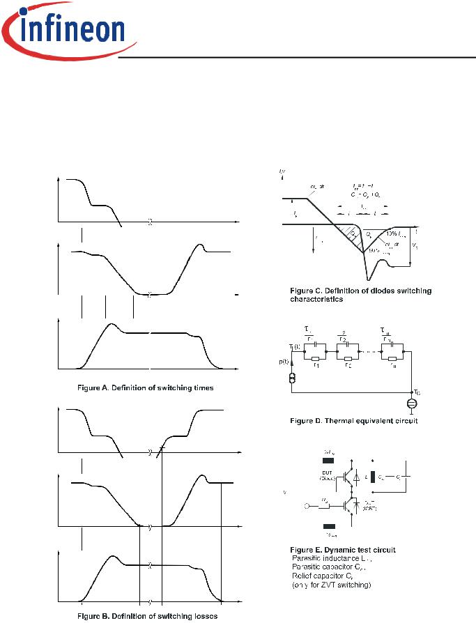
vGE(t)
90% VGE
iC(t)
90% IC
10% IC
vCE(t)
|
td(off) |
|
tf |
|
|
|
|
|
|
||
|
|
|
|
||
|
|
|
|
||
|
|
|
|
|
|
vGE(t)
90% VGE
iC(t)
2% IC
vCE(t)
t2
Eoff =t1∫VCE x IC x dt
t1 |
t2 |
|
|
|
|
a |
b |
|
10% VGE |
a |
b |
||
|
t |
|
|||
|
|
|
|
|
|
|
|
|
90% IC |
|
|
|
|
|
|
|
|
|
|
10% IC |
t |
|
|
|
|
|
|
|
|
|
|
|
|
|
|
|
|
|
|
|
|
τ
|
td(on) |
|
tr |
|
t |
|
|
|
|||
|
|
|
|
||
|
|
|
|
|
|
10% VGE |
t |
|
CC 
t
|
t4 |
|
|||
Eon = |
VCE x IC x dt |
|
|||
t3∫ |
|
|
2% VCE |
t |
|
t3 |
t4 |
||||
|
|||||
17 |
Rev. 1.2, 2013-12-18 |

IKW40N65H5, IKP40N65H5
High speed switching series fifth generation
Revision History
IKW40N65H5, IKP40N65H5
Revision: 2013-12-18, Rev. 1.2
Previous Revision
Revision |
Date |
Subjects (major changes since last revision) |
|
|
|
1.1 |
2012-11-09 |
Preliminary data sheet |
|
|
|
1.2 |
2013-12-18 |
New Marking Pattern |
|
|
|
We Listen to Your Comments
Any information within this document that you feel is wrong, unclear or missing at all ?
Your feedback will help us to continuously improve the quality of this document.
Please send your proposal (including a reference to this document) to: erratum@infineon.com
Published by
Infineon Technologies AG
81726 Munich, Germany
81726 München, Germany
© 2014 Infineon Technologies AG All Rights Reserved.
Legal Disclaimer
The information given in this document shall in no event be regarded as a guarantee of conditions or characteristics. With respect to any examples or hints given herein, any typical values stated herein and/or any information regarding the application of the device, Infineon Technologies hereby disclaims any and all warranties and liabilities of any kind, including without limitation, warranties of non-infringement of intellectual property rights of any third party.
Information
For further information on technology, delivery terms and conditions and prices, please contact the nearest Infineon
Technologies Office (www.infineon.com).
Warnings
Due to technical requirements, components may contain dangerous substances. For information on the types in question, please contact the nearest Infineon Technologies Office.
The Infineon Technologies component described in this Data Sheet may be used in life-support devices or systems and/or automotive, aviation and aerospace applications or systems only with the express written approval of Infineon Technologies, if a failure of such components can reasonably be expected to cause the failure of that life-support, automotive, aviation and aerospace device or system or to affect the safety or effectiveness of that device or system. Life support devices or systems are intended to be implanted in the human body or to support and/or maintain and sustain and/or protect human life. If they fail, it is reasonable to assume that the health of the user or other persons may be endangered.
18 |
Rev. 1.2, 2013-12-18 |