

 ATtiny2313A/4313
The OCR1A Register however, is double buffered. This feature allows the OCR1A I/O location to be written anytime. When the OCR1A I/O location is written the value written will be put into the OCR1A Buffer Register. The OCR1A Compare Register will then be updated with the value in the Buffer Register at the next timer clock cycle the TCNT1 matches TOP. The update is done at the same timer clock cycle as the TCNT1 is cleared and the TOV1 flag is set.
Using the ICR1 Register for defining TOP works well when using fixed TOP values. By using ICR1, the OCR1A Register is free to be used for generating a PWM output on OC1A. However, if the base PWM frequency is actively changed (by changing the TOP value), using the OCR1A as TOP is clearly a better choice due to its double buffer feature.
In fast PWM mode, the compare units allow generation of PWM waveforms on the OC1x pins. Setting the COM1x1:0 bits to two will produce a non-inverted PWM and an inverted PWM output can be generated by setting the COM1x1:0 to three (see Table 12-2 on page 111). The actual OC1x value will only be visible on the port pin if the data direction for the port pin is set as output (DDR_OC1x). The PWM waveform is generated by setting (or clearing) the OC1x Register at the compare match between OCR1x and TCNT1, and clearing (or setting) the OC1x Register at the timer clock cycle the counter is cleared (changes from TOP to BOTTOM).
The PWM frequency for the output can be calculated by the following equation:
f fclk_I/O
OCnxPWM = ----------------------------------
N (1 + TOP)
The N variable represents the prescaler divider (1, 8, 64, 256, or 1024).
The extreme values for the OCR1x Register represents special cases when generating a PWM waveform output in the fast PWM mode. If the OCR1x is set equal to BOTTOM (0x0000) the output will be a narrow spike for each TOP+1 timer clock cycle. Setting the OCR1x equal to TOP will result in a constant high or low output (depending on the polarity of the output set by the COM1x1:0 bits.)
A frequency (with 50% duty cycle) waveform output in fast PWM mode can be achieved by setting OCF1A to toggle its logical level on each compare match (COM1A1:0 = 1). The waveform generated will have a maximum frequency of fOC1A = fclk_I/O/2 when OCR1A is set to zero (0x0000). This feature is similar to the OCF1A toggle in CTC mode, except the double buffer feature of the Output Compare unit is enabled in the fast PWM mode.
12.8.4Phase Correct PWM Mode
The phase correct Pulse Width Modulation or phase correct PWM mode (WGM13:0 = 1, 2, 3, 10, or 11) provides a high resolution phase correct PWM waveform generation option. The phase correct PWM mode is, like the phase and frequency correct PWM mode, based on a dualslope operation. The counter counts repeatedly from BOTTOM (0x0000) to TOP and then from TOP to BOTTOM. In non-inverting Compare Output mode, the Output Compare (OC1x) is cleared on the compare match between TCNT1 and OCR1x while upcounting, and set on the compare match while downcounting. In inverting Output Compare mode, the operation is inverted. The dual-slope operation has lower maximum operation frequency than single slope operation. However, due to the symmetric feature of the dual-slope PWM modes, these modes are preferred for motor control applications.
The PWM resolution for the phase correct PWM mode can be fixed to 8-, 9-, or 10-bit, or defined by either ICR1 or OCR1A. The minimum resolution allowed is 2-bit (ICR1 or OCR1A set to
101
8246B–AVR–09/11
0x0003), and the maximum resolution is 16-bit (ICR1 or OCR1A set to MAX). The PWM resolution in bits can be calculated by using the following equation:
RPCPWM = |
log(TOP + 1) |
----------------------------------log(2) |
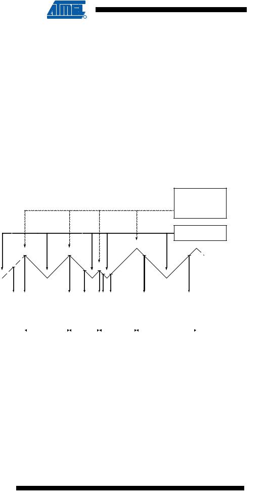
In phase correct PWM mode the counter is incremented until the counter value matches either one of the fixed values 0x00FF, 0x01FF, or 0x03FF (WGM13:0 = 1, 2, or 3), the value in ICR1 (WGM13:0 = 10), or the value in OCR1A (WGM13:0 = 11). The counter has then reached the TOP and changes the count direction. The TCNT1 value will be equal to TOP for one timer clock cycle. The timing diagram for the phase correct PWM mode is shown on Figure 12-8 on page 102. The figure shows phase correct PWM mode when OCR1A or ICR1 is used to define TOP. The TCNT1 value is in the timing diagram shown as a histogram for illustrating the dual-slope operation. The diagram includes non-inverted and inverted PWM outputs. The small horizontal line marks on the TCNT1 slopes represent compare matches between OCR1x and TCNT1. The OC1x interrupt flag will be set when a compare match occurs.
Figure 12-8. Phase Correct PWM Mode, Timing Diagram
OCRnx/TOP Update and OCnA Interrupt Flag Set or ICFn Interrupt Flag Set (Interrupt on TOP)
TOVn Interrupt Flag Set (Interrupt on Bottom)
TCNTn
OCnx |
|
|
|
|
|
|
|
|
|
|
|
|
|
|
|
|
|
|
|
|
|
|
|
|
|
|
|
(COMnx1:0 = 2) |
|
|
|
|
|
|
|
|
|
|
|
|
|
|
|
|
|
|
|
|
|
|
|
|
|
|
|
|
|
|
|
OCnx |
|
|
|
|
|
|
|
|
|
|
|
|
|
|
|
|
|
|
|
|
|
|
|
|
|
|
(COMnx1:0 = 3) |
||
|
|
|
|
|
|
|
|
|
|
|
|
|
|
|
|
|
|
|
|
|
|
|
|
|
|
|
|
|
|
Period |
|
|
|
|
|
|
|
|
|
|
|
|
|
|
|
|
|
|
|
|
|
|
|
||||||
|
|
|
|
|
|
|
|
|
|
|
|
|
|
|
|
|
|
|
|
|
|
|
|
||||||
|
|
|
1 |
|
|
|
|
2 |
|
|
|
|
3 |
|
|
|
|
|
4 |
|
|
|
|
||||||
|
|
|
|
|
|
|
|
|
|
|
|
|
|
||||||||||||||||
|
|
|
|
|
|
|
|
|
|
|
|
|
|
|
|
|
|
|
|
|
|
|
|
|
|
|
|
|
|
The Timer/Counter Overflow Flag (TOV1) is set each time the counter reaches BOTTOM. When either OCR1A or ICR1 is used for defining the TOP value, the OCF1A or ICF1 flag is set accordingly at the same timer clock cycle as the OCR1x Registers are updated with the double buffer value (at TOP). The interrupt flags can be used to generate an interrupt each time the counter reaches the TOP or BOTTOM value.
When changing the TOP value the program must ensure that the new TOP value is higher or equal to the value of all of the Compare Registers. If the TOP value is lower than any of the Compare Registers, a compare match will never occur between the TCNT1 and the OCR1x. Note that when using fixed TOP values, the unused bits are masked to zero when any of the OCR1x Registers are written. As the third period shown in Figure 12-8 illustrates, changing the TOP actively while the Timer/Counter is running in the phase correct mode can result in an unsymmetrical output. The reason for this can be found in the time of update of the OCR1x Register. Since the OCR1x update occurs at TOP, the PWM period starts and ends at TOP. This
102 ATtiny2313A/4313
8246B–AVR–09/11

 ATtiny2313A/4313
implies that the length of the falling slope is determined by the previous TOP value, while the length of the rising slope is determined by the new TOP value. When these two values differ the two slopes of the period will differ in length. The difference in length gives the unsymmetrical result on the output.
It is recommended to use the phase and frequency correct mode instead of the phase correct mode when changing the TOP value while the Timer/Counter is running. When using a static TOP value there are practically no differences between the two modes of operation.
In phase correct PWM mode, the compare units allow generation of PWM waveforms on the OC1x pins. Setting the COM1x1:0 bits to two will produce a non-inverted PWM and an inverted PWM output can be generated by setting the COM1x1:0 to three (See Table 12-3 on page 111). The actual OC1x value will only be visible on the port pin if the data direction for the port pin is set as output (DDR_OC1x). The PWM waveform is generated by setting (or clearing) the OC1x Register at the compare match between OCR1x and TCNT1 when the counter increments, and clearing (or setting) the OC1x Register at compare match between OCR1x and TCNT1 when the counter decrements. The PWM frequency for the output when using phase correct PWM can be calculated by the following equation:
fOCnxPCPWM = |
fclk_I/O |
2---------------------------N TOP |
The N variable represents the prescaler divider (1, 8, 64, 256, or 1024).
The extreme values for the OCR1x Register represent special cases when generating a PWM waveform output in the phase correct PWM mode. If the OCR1x is set equal to BOTTOM the output will be continuously low and if set equal to TOP the output will be continuously high for non-inverted PWM mode. For inverted PWM the output will have the opposite logic values.
12.8.5Phase and Frequency Correct PWM Mode
The phase and frequency correct Pulse Width Modulation, or phase and frequency correct PWM mode (WGM13:0 = 8 or 9) provides a high resolution phase and frequency correct PWM waveform generation option. The phase and frequency correct PWM mode is, like the phase correct PWM mode, based on a dual-slope operation. The counter counts repeatedly from BOTTOM (0x0000) to TOP and then from TOP to BOTTOM. In non-inverting Compare Output mode, the Output Compare (OC1x) is cleared on the compare match between TCNT1 and OCR1x while upcounting, and set on the compare match while downcounting. In inverting Compare Output mode, the operation is inverted. The dual-slope operation gives a lower maximum operation frequency compared to the single-slope operation. However, due to the symmetric feature of the dual-slope PWM modes, these modes are preferred for motor control applications.
The main difference between the phase correct, and the phase and frequency correct PWM mode is the time the OCR1x Register is updated by the OCR1x Buffer Register, (see Figure 12- 8 on page 102 and Figure 12-9 on page 104).
The PWM resolution for the phase and frequency correct PWM mode can be defined by either ICR1 or OCR1A. The minimum resolution allowed is 2-bit (ICR1 or OCR1A set to 0x0003), and the maximum resolution is 16-bit (ICR1 or OCR1A set to MAX). The PWM resolution in bits can be calculated using the following equation:
RPFCPWM = |
log (TOP + 1) |
----------------------------------log (2) |
103
8246B–AVR–09/11
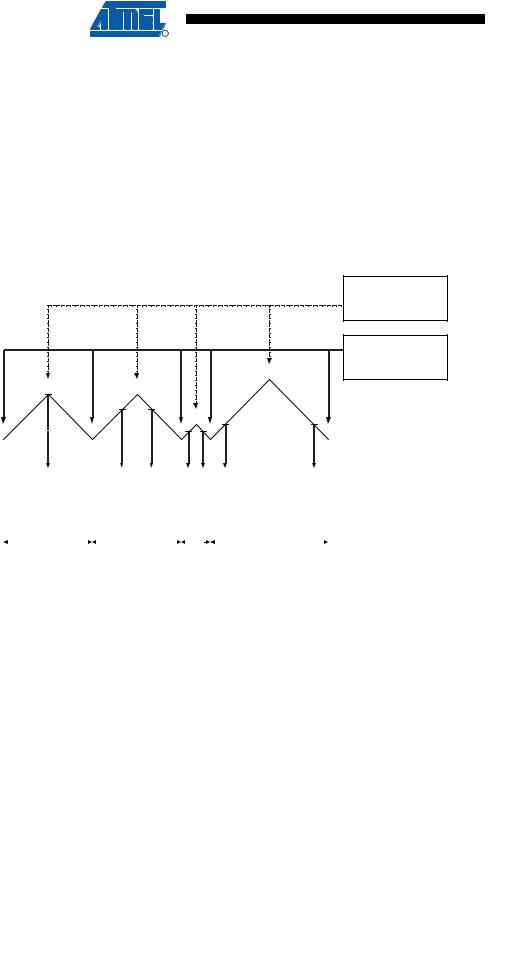
In phase and frequency correct PWM mode the counter is incremented until the counter value matches either the value in ICR1 (WGM13:0 = 8), or the value in OCR1A (WGM13:0 = 9). The counter has then reached the TOP and changes the count direction. The TCNT1 value will be equal to TOP for one timer clock cycle. The timing diagram for the phase correct and frequency correct PWM mode is shown on Figure 12-9 on page 104. The figure shows phase and frequency correct PWM mode when OCR1A or ICR1 is used to define TOP. The TCNT1 value is in the timing diagram shown as a histogram for illustrating the dual-slope operation. The diagram includes non-inverted and inverted PWM outputs. The small horizontal line marks on the TCNT1 slopes represent compare matches between OCR1x and TCNT1. The OC1x interrupt flag will be set when a compare match occurs.
Figure 12-9. Phase and Frequency Correct PWM Mode, Timing Diagram
OCnA Interrupt Flag Set or ICFn Interrupt Flag Set (Interrupt on TOP)
OCRnx/TOP Updateand TOVn Interrupt Flag Set (Interrupt on Bottom)
TCNTn
OCnx |
|
|
|
|
|
|
|
|
|
|
|
|
|
|
|
|
|
|
|
|
|
|
|
|
(COMnx1:0 = 2) |
|
|
|
|
|
|
|
|
|
|
|
|
|
|
|
|
|
|
|
|
|
|
|
|
|
|
|
|
OCnx |
|
|
|
|
|
|
|
|
|
|
|
|
|
|
|
|
|
|
|
|
|
|
|
|
(COMnx1:0 = 3) |
|
Period |
|
|
|
|
|
|
|
|
|
|
|
|
|
|
|
|
|
|
|
|
|
|
|
|
|
|
|
|
|
|
|
|
|
|
|
|
|
|
|
|
|
|
|
|
|
|
|
|
|
||||
|
|
|
|
|
|
|
|
|
|
|
|
|
|
|
|
|
|
|
|
|
|
|
||||
|
|
1 |
|
|
|
|
|
2 |
|
|
|
|
|
3 |
|
|
|
4 |
|
|
|
|
||||
|
|
|
|
|
|
|
|
|
|
|
|
|
|
|||||||||||||
|
|
|
|
|
|
|
|
|
|
|
|
|
|
|
|
|
|
|
|
|
|
|
|
|
|
|
The Timer/Counter Overflow Flag (TOV1) is set at the same timer clock cycle as the OCR1x Registers are updated with the double buffer value (at BOTTOM). When either OCR1A or ICR1 is used for defining the TOP value, the OCF1A or ICF1 flag set when TCNT1 has reached TOP. The interrupt flags can then be used to generate an interrupt each time the counter reaches the TOP or BOTTOM value.
When changing the TOP value the program must ensure that the new TOP value is higher or equal to the value of all of the Compare Registers. If the TOP value is lower than any of the Compare Registers, a compare match will never occur between the TCNT1 and the OCR1x.
As Figure 12-9 shows the output generated is, in contrast to the phase correct mode, symmetrical in all periods. Since the OCR1x Registers are updated at BOTTOM, the length of the rising and the falling slopes will always be equal. This gives symmetrical output pulses and is therefore frequency correct.
Using the ICR1 Register for defining TOP works well when using fixed TOP values. By using ICR1, the OCR1A Register is free to be used for generating a PWM output on OC1A. However, if the base PWM frequency is actively changed by changing the TOP value, using the OCR1A as TOP is clearly a better choice due to its double buffer feature.
In phase and frequency correct PWM mode, the compare units allow generation of PWM waveforms on the OC1x pins. Setting the COM1x1:0 bits to two will produce a non-inverted PWM and
104 ATtiny2313A/4313 
8246B–AVR–09/11