

subvolt
.pdftunnel transistors with Vdd ≈0.2 V[47,48], quantum interference effect molecular transistors[49], integrated emitters and sensors of terahertz radiation[50-52], nanotube-based ones included [53], atomic switches with quantum conductivity based on solid state ionic conductors [54], memristors[55], etc. The nano-epitaxy method of semiconductor fabrication with a high-quality crystal structure makes it possible to combine different highly functional materials within one system [56].
Algorithms of information processing
Systems: SoC, 3D, SiP, NMSE, nanomorphic cell
Topology of integrated circuits
Design methodology of integrated circuits
Types and classes of devices
Technologies
Materials
New carriers and ways for information processing and transmission
Thermodynamics Quantum Electrodynamics mechanics
Fig. 4. Hierarchy of levels determining energy consumption per 1 bit processing.
At the level of IC design methodology, integrated digital cellular automata[57], adaptive and defect-tolerant self-organizing, self-healing networks that implement massively parallel computations [58], crossbar 3D and hybrid structures [59,60] look definitely promising. At the level of systems, built-in devices, e.g. for brain-machine interfaces, large-scale distributed complex systems for health, security and environment (nano-tera networks) pose tremendous challenges in various areas of information processing, see Ref. 61 for more details. In Ref. 62, the possibility of creating «nanomorphic cell» of a 10 m characteristic size integrated at the atomic level was discussed. Such systems equipped with an energy sources [63] should interact with living cells, analyze data (computing), and be able to exchange information. In Ref. 64 a thin-film Mach-Zehnder intensity modulator operating at 0.3 V was developed, which is an important step toward integration of DSVN and deep-sub-voltage electro-optical heterostructures. For «1012-1012» IC architectures, a critical problem is to describe closely placed nanodevices operating in the ballistic or tunnel mode because certain values of capacitance, inductance and resistance cannot be attributed to them.
In NRI [65], major attention is concentrated on the search for novel information carriers [66] and methods of data transfer and processing. Some works analyze the basic principles of nanodevice functioning and capacity of information channels [67,68], determine ways to obtain transistor current characteristics below Vg =kBTln10/e (300 K) =60 mV/decade I [69,70], discuss possible applications of spin waves to perform logic operations [56], and make estimates of quantum limits for energy dissipation in spintronics. Computation is a physical process which occurs in a material subsystem (a nanotransistor) embedded in a thermostat (semiconductor crystal) [28]. It was shown in Ref. 71 that under the conditions when a thermodynamic equilibrium between a device and a thermostat is not reached (the device sizes and the time of switching are of the order characteristic of thermal processes), the dissipated power can be smaller than in the case of the Boltzmann equilibrium distribution.
An estimate of the optimal effective mass of information carriers by the Q-factor in nanotransistors of binary logics with a gate channel length decreasing below 5 nm was made in Ref. 66. The Q-factor is the ratio of the time a device is in the state 1
or 0 (τstore) to the time of transition process 1↔0 (tsw), it determine the ratio (Ion/Ioff) and probability of correct performance of a logic operation.
Q |
store |
|
|
h |
|
|
exp |
|
|
exp |
|
|
|
|
|
|
|
|
Eb |
|
|||
|
|
|
|
|
|
|
|
|
|
|
|
|
tsw |
|
|
|
|
|
|
|
kBT |
||
|
|
L 2m* E |
|
||||||||
|
|
|
g |
b |
|
|
|
|
|||
2 2E
b Lg
|
|
|
|
Eb |
|
|
|
|
m* |
exp |
|
exp |
|
||||
|
|
|||||||
|
|
|
|
|
|
|
||
|
|
|
|
kBT |
|
|
||
|
|
|
|
|
1 |
|
|
2 2Eb |
|
|
|||||
Lg |
m* |
, |
(2) |
||||
|
|||||||
|
|
|
|
|
|||
|
|
|
|
|
|
|
|
where Lg is the gate length , m* is the effective mass of information carriers, Eb is the potential barrier height, T is the temperature, kB is the Boltzmann constant, and h = 2 is the Plank constant (6.6∙10-34 J s-1). According to Eq. (2) [66], silicon field effect transistors with Eb =0.75 eV (high-performance ICs) cannot be used at Lg ≤5 nm (Q –factor is small because of m* smallness). However, in DSVN where Eb ≤0.25 eV, silicon meets the requirements of nanotransistors fabricated with Lg ≤ 5 nm (figure 5).
21
|
1 |
Eb=0.75 eV, Lg=10 nm |
3 |
Eb=0.25 eV, |
Lg=10 nm |
|
|
||
|
2 |
Eb=0.75 eV, |
Lg=5 nm |
4 |
Eb=0.25 eV, |
Lg=5 nm |
|
|
|
|
1,50E+012 |
|
|
|
|
|
|
15000 |
|
|
|
|
|
|
|
|
2 |
|
|
|
1,00E+012 |
|
|
|
|
|
|
10000 |
|
|
|
|
|
|
|
|
|
|
|
Q -factor |
|
|
|
|
|
|
4 |
|
factor- Q |
5,00E+011 |
|
|
|
|
|
1 |
5000 |
||
|
|
|
|
|
|
|
|
|
|
|
|
|
m*Si |
|
|
3 |
|
|
|
|
|
|
|
|
|
0 |
|
||
|
0,00E+000 |
|
|
|
|
|
|
|
|
|
|
|
|
|
|
|
|
|
|
|
|
0,0 |
0,2 |
0,4 |
0,6 |
0,8 |
1,0 |
|
|
|
|
|
|
m* /m |
|
|
|
|
|
|
|
|
|
|
e |
|
|
|
|
Fig. 5. Q –factor dependence on the effective mass m* of information carriers in short channel field effect transistors. Calculated by formula (2), see Ref. 66 for more details:
1 - Eb =0.75 eV, Lg =10 nm; 2 - Eb =0.75 eV, Lg =5 nm; 3 - Eb =0.25 eV, Lg =10 nm; 4 - Eb =0.25 eV, Lg =5 nm.
In DSVN the portion of application-specific ICs must be large because of (i) a large number of approaches to obtaining limit values of ε (figure 4), (ii) a wide range of science and technological directions (microand nanosystem engineering, wireless networks of microsensors and microrobots, RFID, bio-medical applications, etc.) which require autonomous and energy-saving ICs of the “system on chip” type, and (iii) high-functionality of a chip of < 1mm2 area at the 1011-1012 cm-2 component density. According to (i) and (ii), the number of chips in a application-specific series is relatively small, ~104 -105 and because of (iii) 2- 10 wafers of a 100-200 mm diameter would suffice to fabricate these chips. Therefore, it can be expected that mini-factories with a potential of fast resetting-up of technological processes would be in demand in DSVN. Special attention should be paid to the development of technologies for the creation of high-density (up to 1012 cm-2 double-electrode elements) crossbar structures [72] which do not require electrode layers matching with high precision and have a number of advantages in hybrid configurations with CMOS [59]. In the recent work [73], new materials for functional crossbar structures and a low cost nonlithographic patterning technique for tera-scale integration were considered.
3. High-capacity capacitors for nanoelectronics
In portable devices, surface mount capacitors stand out sharply against other electronic components because of their large size. With the development of nanoelectronics and related technologies, creation of micro-scale capacitors and impulse storage devices with high density of energy ( E), capacitance ( C), and power ( W) has become urgent. Below, we present arguments for the benefits using of all-solid state impulse supercapacitors with fast ion transport (FIT) at functional advanced superionic conductor (AdSIC)/electronic conductor (EC) heterojunctions (nanoionic supercapacitors, NSCs) in sub-voltage and deep-sub- voltage nanoelectronics, space technique, micro(nano)systems, wireless, RFID, high-temperature electronics and some other fields. AdSICs have a crystal structure close to optimal for fast ion transport (FIT). The rigid ion sublattice of AdSIC has structure channels where mobile ions migrate. The ion-transport characteristics of AdSIC are very high: ionic conductivity i ≈0.3 Ohm-1 cm-1 (RbAg4I5, 300 K) and activation energy Ei ≈0.1 eV. This determines the temperature-dependent concentration of mobile ions ni ~Ni exp(-Ei /kBT) capable of migrating in conduction channels at any moment (Ni ≈1022 cm-3, ni ~2∙1020cm-3, 300 K). Time-averaged distribution of mobile Ag+ ions in the channels of ionic conductivity of AdSIC (crystal structure of RbAg4I5) was experimentally obtained in Ref. 74.
The NSCs can be fabricated by microelectronics technologies. The values E and C of NSC are 1-2 decimal orders of magnitude higher than in conventional-type capacitors with thin films of ferroelectric ceramics, SiO2, ZrO2, HfO2, etc. An inherent disadvantage of conventional capacitors is an exponential fast growth of tunnel leakage current at dielectric film thickness less than 2 nm. The frequency range of NSC operation is determined by FIT at functional AdSIC/EC heterojunctions
22
and has a theoretical limit of ~1010 Hz (300 K), which corresponds to the frequency of jumps of mobile ions in AdSIC. High C in NSC (Vdd ~0.5 V) is not associated with tunnel leakage current.
3.1. Field application of sub-voltage high-capacity micro-sized capacitors
In digital electronics, currents i on internal buses of IC increase as frequencies f increase and Vdd decrease. Large i give rise to noise sources whose effect can be minimized by using decoupling capacitors Cdecap. If the dissipated power is P = 100 W, f =1
GHz and Vdd =1.4 V, then Cdecap ~0.5 F [75]. |
|
Cdecap > 10 P∙f -1 ∙V-2dd . |
(3) |
At low Vdd the value of di/dt ≈P∙f ∙V-1dd increases on the loaders. To prevent the voltage of a noise source, determined by di/dt
from increasing with respect to Vdd, the following steps should be taken (i) to increase the area underCdecap (however, this reduces the efficiency and functioning of IC) and (ii) to increase the density of capacitanceC ( F/cm2) and C ( F/cm3) of
Cdecap. For nanodevices, 1/f noise (with spectral density ~ N-1 f -1) is a fundamental challenge (N is the number of electron carriers in a sample). In perfect epitaxial layers, the constant is ~10-6 - 10-4, in defect layers the constant is much higher. For
example, in pMOSFET the 1/f noise increases by 10 to 100 times when the device size decreases from 350 to 130 nm [76]. A complex noise is filtered by several parallel-connected capacitors which differ in relaxation times , capacitance, inductance and equivalent resistance. Capacitors with large and C ( C) values are also used in low-frequency filters, amplifiers, seismic detectors, supply circuits, etc.
Tiny self-sustained objects of critical and advanced technologies require impulse energy and charge storage devices with high E, C and W values. Sub-voltage devices scavenged energy from the environment (light, pressure and temperature gradients, vibration, etc.) and -radioisotope-based microgenerators together with impulse energy and charge storage devices can support long-term operation of portable consumer electronics, wireless microsensors and microrobots networks, picosputnics, RFID, implanted biomedical devices, etc. According to J. Pister, the author of «Smart Dust» conception, autonomous power sources with Vdd ≤ 0.5 V would be used in digital and analog electronics of self-sustained wireless networks with nodes which posses sensor, computation, and communication functions, see Ref. 77 for more details. The incorporation of 3V lithium cells into power units would require step-down DC/DC voltage converters which should contain high-capacity capacitors.
Present-day 0.3 x 0.3 x 0.6 mm RFID chips include structures transforming radio-frequency energy into a direct current. In the simplest case, such a structure is an antenna, a diode, and a reservoir-capacitor ( C ~0.35 F/cm2) determining the operation possibilities of a RFID chip and occupying about S =¼ of total chip area. The capacitance of a RFID chip reservoir-capacitor is
determined by |
|
C ≈ i Δt (Vmax –Vmin)-1 , |
(4) |
where Vmax and Vmin are the limit voltage values, i is an average current on the load in the active stage of functioning, and Δt is the time of data transfer. In a future 0.5 V RFID, ΔV = Vmax – Vmin should be approximately 0.1 V, which radically differs from
ΔV about 1 V in present-day chips. The energy radiated by a RFID-chip C Vmax ΔV and power C VmaxΔV/Δt depend on the distance and radio-exchange protocol. If Vmax decreases by 3 times and ΔV by 10 times, the capacitance should increase by 30
times, so that
C VmaxΔV product be retained, however a C ~0.35 F/cm2 chip has no room to accommodate the required capacitance. Most acceptable would be chip area S about 0.1, but conventional capacitors cannot afford C ~50 F/cm2. Operational frequencies of reservoir-capacitors are to correspond to the frequency of radio exchange. In RFID standards, these are 135 kHz, 13.56 MHz, 2.45 GHz, 860-960 MHz, etc. So, 0.5 V RFID chips require capacitors with an operation frequency in the 105-109 Hz range. The condition C ~50 F/cm2 determines the lower limit C for many types of 0.5 V autonomous devices.
3.2. Modern design of micro-sized capacitors
3.2.1. Ferroelectric structures
For a plane capacitors, the voltage breakdown Fmax, dielectric permittivity k , Vdd , C and C are related as
Vdd ≈Fmax (k∙ε0 / C )1/2 = Fmax k ε0 / C , (5)
where ε0 = 8.85 10-12 F m-1. Therefore, devices with low Vdd require the development of capacitors with limiting-high C ( C) determined by Vdd and tunnel leakage current (an “inherent” disadvantage of capacitors with dielectric layer thickness d less than 2 nm). For sub-voltage electronics, promising are capacitors (i) based on dielectrics with highk (e.g. ZrO2 ,HfO2, La2Hf2O7, etc.) characterized by C ~2 F/cm2 at d ~2 nm Vdd ~1 V [78-80], (ii) having trench structures (large aspect ratios), where the efficient C ≈3 F/cm2 at the SiO2 film thickness 4.5 nm [75] and C > 20 F/cm2 at the formation of dielectric layers with k ≈15...20 [81], and (iii) based on ferroelectric ceramics, e.g. PZTk (≈900), with C ≈3 F/cm2 [82]. In nanoionic supercapacitors (NSC) based on AdSIC, Fmax at the functional AdSIC/EC heterojunctions (d of the atom size) can exceed 107
23
V/cm, therefore in smooth electrodes C ~100 F/cm2[83]. In NSC with trench structures, the effective values of C ~1000F/cm2. The development of ferroelectric-based capacitors (k ~1000) have shown that k decreases considerably in thin films. Multilayer ferroelectric capacitors of ultra dense surface mount in a smallest case (01005 EIA) are of 0.4 x 0.2 x 0.2 mm size and maximum capacitance 0.01 F at Vdd =6.3 V C ≈1 F/mm3 and effective C ≈13 F/cm2[84]. Low-frequency capacitance of epitaxial heterostructures ScRuO3/ScTiO3 is approximately C ≈26 F/cm2 which differs from the nominal value C = ε0∙k/ d =160 F/cm2 at k=490 and d =2.7 nm[85]. In capacitors based on perovskite thin films (5...30 nm), C is usually equal to 12.5...2.5 F/cm2 (k ~70) at Vdd = 0.65...4.0 V [86]. Operation at temperatures higher than 85 oC is becoming conventional for small-size sources. A standard requirement to them is a guaranteed functioning of an electron component for 10 years at 125 oC. Multilayer ferroelectric capacitors operate at frequencies to 109 Hz and provide C ≈3 F/mm3 at the size 1.6 x 0.8 x 0.6 mm. Disadvantages of these capacitors are a reduction of C with increasing F and low stability of ceramics to higher temperatures and F [87]. So, present-day ferroelectric capacitors do not meet the requirements of C ( C) -Vdd scaling and do not suit a number of new high-tech applications related to DSVN.
3.2.2. Miniature tantalum capacitors
High-capacity tantalum capacitors can operate at temperatures to 175 oC. The working voltage decreases with increasing temperature as follows: 6.3 V (85 oC), 4 V (125 oC), 3.2 V (150 oC), and 2.1 V (175 oC). Their capacity decreases in the range 103…104 Hz. When a 01005 case is used instead of a 3216 one, C decreases by 5…10 times (down to C ≈0.17…0.08F/mm3). This effect is also characteristic of ferroelectric miniature capacitors.
3.2.3. Capacitors on the basis of nanodielectrics with k ~107...1010.
A number of works (see Refs. 88 and 89 for more details) present experimental data on capacitors with nanodielectrics which are reportedly characterized by gigantic k ~107-1010 and a large potential in energy storage [89-91]. The analysis of the data does not support the expectations. In a plane capacitor, the surface charge density Q on atomically smooth electrodes is limited by
Qmax ~1.5∙10-4 C/cm2 (an ion charge of one sign on crystallographic planes with small indices, the concentration n ≈1015 cm-2). The value Qmax cannot be exceeded because at Qmax the electric field Fmax ≈ 2 109 V/cm (k=1) has the energy ρE =ε0 F2max/2 ≈170 kJ/cm3 which is several times large than the standard enthalpy of chemical compound formation (e.g. HNaCl ≈ 411
kJ/mol). Thus,
k F Qmax /ε0 ≈1.5 109 V/cm, (6) where F = V/d and V is the voltage on electrodes. According to Eq. (6), at k ~107-1010 the maximum permissible value of Fmax in a nanodielectric must be small (102 -10-1V/cm) as compared to the breakdown field in ordinary dielectrics (≈2 ∙106 V/cm). In
the zero electrode thickness approximation, the maximum energy density in plane capacitors is
ρE ~ ε0 k F2max /2 . |
(7) |
At k Fmax ≈ Qmax /ε0 , Eq. (7) can be written as |
|
ρE < ~ Qmax Fmax/2 , |
(8) |
where Fmax ~102 -10-1 V/cm. This shows that the expectations concerning the application of nanodielectrics with gigantic dielectric permittivity for energy storage are groundless.
3.2.4. Supercapacitors on the basis of liquid electrolytes.
The possibility of using mobile ions for storing charge and energy has been realized in devices with a double electric layer, called supercapacitors. In the case of liquid electrolytes, electrodes with a large internal surface can provide C ~1000 F/mm3 ( C ~15 F/cm2 per the internal surface area [92]), but the frequencies of device operation are low and the design of the devices is incompatible with vacuum technologies.
3.3. Supercapacitors on the basis of advanced superionic conductors (AdSICs)
Record high capacity-frequency characteristics can be obtained using coherent advanced superionic conductor (AdSIC)/electronic conductor (EC) heterojunctions [93]. The general classification of solid state ionic conductors according to their ion-electron conductivities ( i - e) is presented in Fig. 6 [83]. The boundary of the 7-8 area determines the upper limit of i values for hypothetic AdSIC. By definition, these ionic conductors should have Ei ≈kBT (300 K), which is to give i ~2 Ohm-1 cm-1 (mobile Ag+-ions) at 300 K and i~ 8 (20) Ohm-1cm-1 for mobile Li+ (H+) ions.
24
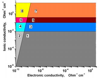
Fig. 6. Classification of solid state ionic conductors in the lg i -lg e coordinates (Ohm-1 cm-1) [83].
2, 4 and 6 – known solid electrolytes (SE), materials
with i >> e;
1, 3, and 5 – known mixed ion-electron conductors;
3 and 4 – superionic conductors (SIC), i.e. materials with i > 0.001 Ohm-1cm-1, e – arbitrary value;
4– SIC and simultaneously SE, i > 0.001 Ohm-1cm-1, i >> e ;
5and 6 – advanced superionic conductors (AdSIC), where
i > 10-1 Ohm-1cm-1 (300 K), Ei 0.1 eV, e – arbitrary value;
6– AdSIC and simultaneously SE, i > 10-1 Ohm-1cm-1, Ei 0.1 eV, i >> e ;
7and 8 – hypothetical AdSIC with Ei ≈ kBT 0.03 eV (300 К);
8– hypothetical AdSIC and simultaneously SE.
The RbAg4I5 family includes a number of AdSIC-SEs with Cu+ or Ag+ mobile ions. Some of these compounds are thermodynamically stable around room temperature ( -RbAg4I5, CsAg4I2-xI3+x, RbCu4Cl3I2, etc.) but the majority of them are stable at higher temperatures (50-120 oC). AdSIC-SE–based supercapacitors have already been developed for several decades (their radiation stability can be very high), however, the C of their heterojunctions (with arbitrary, structure-uncontrolled AdSIC/EC heteroboundaries) is 102 -101 F/cm2 at frequencies 10-2-103 Hz. Low operation frequencies of AdSIC/EC heterojunctions and, hence, low W of supercapacitors are the result of fast ion transport violation in molecular-thin layer at the AdSIC/SE heteroboundaries. The product of maximum operation frequency fмах of AdSIC/EC heterojunction by C is a generalized characteristic of capacity and frequency parameters. For typical heterojunctions, e.g. RbAg4I5/Pt [94], this product fмах∙ C is ~ 1 -104 Hz F/cm2. For heterojunctions with liquid electrolytes, the fмах∙ C product is of the same order of magnitude. Research and development in nanoionics of AdSIC, a new science and technological field, have been carried on at the Institute of Microelectronics Technology RAS for several years[93]. The object of these investigations is nanoand microstructures based on AdSIC. AdSIC/EC heterojunctions are key functional structures in all-solid-state supercapacitors. Therefore the major approach to AdSIC nanoionics is to retain the concentration and potential barrier heights to mobile ion jumps on heteroboundaries at the level of those in AdSIC volume.
4. Nanoionic supercapacitors
High values of fмах∙ C on AdSIC/EC heterojunctions can be obtained under certain conditions. These are (i) to form an atomically clear and sharp AdSIC/EC contact, (ii) to provide small disordering ofethstructure in an AdSIC layer adjacent to EC, which can be realized on the AdSIC/EC coherent boundaries, and (iii) to provide a certain combination and mutual arrangement of crystal symmetry elements of the AdSIC/EC heteroboundary and symmetry elements of fast ion transport channels in the AdSIC structure. To this end, methods of crystallochemical design of AdSIC/EC heteroboundaries were employed see Refs. 93 and 95. AdSIC/EC heterostructures (prototypes of NSC) were developed and synthesized with C ≈100
F/cm2 and fмах up to 106 Hz (record high values of the product fмах∙ C ~108 Hz F/cm2) [83].
Frequency-capacity characteristics were registered by comparing “charge-discharge” oscillograms for an experimental twoelectrode cell and a standard capacitor [83]. The -impulses of an external voltage were applied to a circuit consisting of the
25

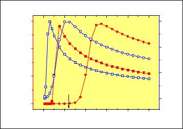
experimental cell (or a standard capacitor) and a ballast resistor R connected in series. The experimental cell of ≈0.0036 mm3 volume (ultra dense surface mount component in the smallest case 01005 EIA has the volume ≈0.016 mm3) had thin film electrodes of the total area ≈0.08 mm2 (0.04 mm2 + 0.04 mm2). The cell thickness was ≈0.03 mm, the area of the cell footprint on the Si-substrate ~0.12 mm2. Voltage changes during “charge-discharge” processes in the experimental cell and the standard capacitor are shown in Fig. 7. Changes in the charge (discharge) time were set by the ballast resistor R. The effective C in the experimental cell is ≈1 F/mm2 (100 F/cm2) at frequencies to ≤106 Hz (Fig. 7) and the power density W ≈0.3 W/mm3 (3∙102 W/cm3). This is 3 times large than in those massive supercapacitors which have distributed carbon electrodes impregnated with a liquid electrolyte (volume ~1 cm3, Vdd ≈2.5 -2.7 V, operation frequencies not higher than fмах < 103 Hz). The energy density E in the cell is ≈10-4 J/mm3 (10-1 J/cm3). This is 36 times smaller than in massive supercapacitors where the product W ∙ E ~4∙102 J2 /s cm6 (in the cell, this product is 10 times smaller). However, the volume can be reduced by 10 times with the stored energy and generated power retained at the same level by changing the cell design. As a result, the product W ∙ E could exceed that in massive supercapacitors by ≈10 times at a volume of ≈0.0004 mm3.
Experiments with a ≈0.0036 mm3 cell showed [83] that (i) effective capacitance densityC depends rather weakly on f up to frequencies ≈106 Hz, (ii) the cell can operate for a long time at 70–170 оС, and (iii) C ≈1 F/mm2, C >10 F/mm3, W ≈0.3 W/mm3, and E ≈ 10-4 J/mm3 can be obtained at frequencies ≈106 Hz. So, film impulse capacitors based on AdSIC are promising devices for deep-sub-voltage nanoelectronics and related technologies.
Fig. 7. Time dependence of the voltage (horizontal scale 1 s/div) during the charge-discharge process in the two-terminal experimental cell and the 0.047 F capacitor through the ballast resistor R=100 Ohm: 1) cell at 155 oC; 2) 0.047 F capacitor connected in series to the resistor r =10 Ohm (vertical scale 100 mV/Div; 3) voltage from an external generator (vertical scale 500 mV/div) for the cases (1) and (2) [83].
Below a model for large C on the heterojunction AdSIC/EC is presented. It is based on three assumptions (i) the formation of an atomically sharp AdSIC/EC heteroboundary, (ii) EC wave function penetration into AdSIC with the formation of charge distribution equivalent to an atomically thin double electric layer by capacity, and (iii) strong shift polarization effect (large values of permittivity k ) of mobile ions of AdSIC. Now consider the (i)-(iii) assumption in detail.
It is known that metal-induced gap states exist on an atomically ordered alkali halide crystal (AHC)/metal (Cu,Ag) heteroboundary, see Refs. 96 and 97 for more details. These states are due to a quantum-mechanical proximity effect between a metal and AHC. The penetration depth of states in AHC (lp) depends on the halide. The values of lp increase with a decrease of the AHC band gap and are 0.3-0.4 nm. This mainly concerns F Cl Br I substitutions in the AHCs. The formation of metal induced gap states on the insulator (semiconductor) heteroboundary is a common-place event [98]. According to Ref. 99, there exist metal induced gap states of the conductivity band character (electron density transfer from a metal to an insulator) and states of the valence band character (electron density transfer from an insulator to a metal). The penetration of electron density into AdSIC (e.g. RbAg4I5) can cause the redistribution of electron density and formation the layer with opposite charge separation ~ lp thick. The electric field (positive sign of potential on EC) in this layer would polarize AdSIC at the interface.
In an external electric field, polarization in crystals with an ionic character of chemical bonding depends on the values of ion displacements from equilibrium positions. These displacements depend on the parameters of a crystal potential relief (coordinate derivative of the crystal potential). In AHC the potential well depth for ions is ~3 eV, which limits permittivity k to ≈5. In AdSIC RbAg4I5–family, the potential wells for mobile ions Ag+ and Cu+ are ~0.1 eV deep. Therefore, k values in AdSIC
26
should be significantly greater than in AHCs. This gives k ~50 for AdSIC, which agrees with the data Ref. 100. Note, that ferroelectric polarization in BaTiO3 ( Q ~2.5 10-5 C/cm2, k ~5000, elementary cell parameter ≈0.4 nm) arises at an ion displacement by ~0.02 nm [101], which is 10 times smaller than a supposed thickness of the double layer on the AdSIC/EC heteroboundary. A plane capacitor with the electrode separation lp ~0.2-0.3 nm and k ~50 has C ~ε0 k/lp>100 F/cm2, which agrees with the experimental data Ref. 83.
In the last few years the performance of INTEL processors mainly rises due to an increase in the component density rather than to an increase in the clock frequency (overheating of ICs, see the figure 1b in Ref. 26). It was noted in Ref. 102 that the operation frequency of ICs with the component density 1012 cm-2 and Vdd~0.5 V would be ~107 Hz unless the problem of thermal overheating of ICs is solved. It follows that the upper limit of time permissible for dielectric relaxation processes on AdSIC/EC functional heterojunctions may be ~10-7 s in DSVN, which would facilitate the creation of devices on the basis of AdSIC. The chemical composition and crystal structure at the AdSIC/EC heterojunctions should be regarded as additional “fields” determining the k value and ion-transport characteristics in nanoionic devices (nanodevices with fast ion transport). Crystal engineering methods and self-organization principles in AdSIC nanosystems (see Refs. 93 and 95 for more details) can become the basis for the creation of capacitors with record high frequency-capacity characteristics.
The figure of merit of an IC planar design is the flop rate per unit area, i.e. the transistor switching frequency and component density product. Reservoir capacitors shrink chip area available for logic and memory. Therefore, the order of NSC market cost
magnitude can be evaluated by the following formula:
VNSC = NjIC AjIC S , (9)
where VNSC is the NSC gross cost, j is the market sector index, NjIC is the number of IC produced, AjIC is an average price of one IC, and S is an average fraction of the IC area taken by NSC. For example, in the RFID sector, the reservoir capacitor of the
power unit in modern IC takes approximately ¼ of the area, therefore S≈0.25 according to Eq. (9). The prognosis of Ref. 103 for the period 2006-2016 says that the RFID market would increase by 10 times to cost NRIC ARIC ~$ 26∙109.
5. Conclusion
Phenomena, properties, effects, mechanizms of processes and applications connected with fast ion transport in all-solid state nano-objects and nanosystems are a subject matter of nanoionics [93, 104,105] which has areas intersecting with nanoelectronics and related technologies. Functional elements with fast ion transport at a nanoscale exist in nanoionic supercapacitors and lithium and fuel cells (nanostructured electrodes) [106]. Switches on the basis of solid state ionic conductors realizing quantum conductance are nanoionic devices [107-109]. ITRS [7] relates the resistive ionic crossbar memory [107-109] to a category of «emerging research devices». By Vdd, nanoionic heterostructures and devices are well suited to a future deep-sub-voltage nanoelectronics and can find unexpected applications. For example, a strong electric field exceeding 107 V/cm can be easily sustained at the interface AdSIC/semiconductor and this effect can be used for efficient modulation of current flow in the channel of future field effect transistors operating at frequencies of approximately 107 Hz (ICs with component densities up to 1012 cm-2).
At present, the vision of future nanoelectronics, constrained solely by fundamental ultimate limits, is being formed in advanced researches, Refs. 29, 39 and 110. Ultimate physical limits to computation [111] are very far off from the present-day attained «1010 -1010» region. What kind of logic switches might be used at the near nmand sub-nm peta-scale integration? The question was already under consideration in the work [112] where the term “nanoelectronics” (Bate R. T., Reed M. A., Frazier G.A. and Frensley W. R., 1987-1989) was not used yet. Quantum mechanics constrains electronic distinguishable configurations by the tunneling effect at the tera-scale. To overcome the 1012 cm-2 bit density limit, atomic and ion configurations with a characteristic dimension of L <2 nm should be used in the information domain and the materials with an effective mass of information carriers m* considerably large than electronic one are required, m* =13me at L =1 nm, m* =53me (L =0.5 nm) and m* =336me (L =0.2 nm) [66]. Future ultimate short-sized devices mat well be nanoionic, i.e. based on the fast ion transport at the nanoscale, as it was first proposed in [105]. Memristors [55,113], hybrid devices that rely on the movement of both electrons and ions and exploiting both classical and quantum charge transport [114], are a step towards future deep-sub- voltage nanoionics.
In conclusion, we would like to cite philosophical view related to nano-world: «The natural scaling process has already led
us to the realm of nanotechnology and nanoelectronics where both difficult technical challenges and golden opportunities co-exist» [6].
Acknowledgments
The authors would like to thank V.V. Zhirnov and R.K. Cavin for the preprints of works on the «nanomorphic cell».
27
References
1.R.T. Bate, G.A. Frazier, W.R. Frensley and M.A. Reed, Texas Instrument Technical Journal: Special Issue on Nanoelectronics 6, #4, 13 (1989).
2.J.H. Luscombe and W.R. Frensley, Nanotechnology 1, 131 (1990).
3.M.P. Frank, Quantum Information Processing 4, 283 (2005).
4.J. Gruska, Natural Computing 6, 75 (2007).
5.J.N. Randall, M.A. Reed and G.A. Frazier, J. Vac. Technol.B 7, 1398 (1989).
6.R. Chau, B. Doyle, S. Datta, J. Kavalieros and K. Zhang, Nature Materials 6, 810 (2007).
7.http://www.itrs.net/home/html
8.P. Tsipas, S. N. Volkos, A. Sotiropoulos, S. F. Galata, G. Mavrou, D. Tsoutsou, Y. Panayiotatos, A. Dimoulas, C. Marchiori and J. Fompeyrine, Appl. Phys. Lett. 93, 082904 (2008).
9.E.-H. Toh, G.H. Wang, L. Chan, G. Samudra and Y-C. Yeo, Semicond. Sci. Technol. 23, 015012 (2008).
10.S. Xin, L. Qiang, V. Moroz, H. Takeuchi, G. Gebara, J. Wetzel, S. Ikeda, C. Shin and Tsu-Jae King Liu, IEEE Electron Device Lett. 29, 491 (2008).
11.G.P. Lansbergen, R. Rahman, C.J. Wellard, I. Woo, J. Caro, N. Collaert, S. Biesemans, G. Klimeck, L.C.L. Hollenberg and S. Rogge, Nature Physics 4, 656 (2008).
12.K. Natoti and N. Sano, J. Appl. Phys. 83, 5019 (1998).
13.R. K. Cavin and V. V. Zhirnov, Morphic architectures: Atomic-level limits, Mater. Res. Soc. Symp. Proc. Materials and Devices for “Beyond CMOS” Scaling (2008), 1067E pp. B01-02.
14.M. Asada, Photonic Based on Wavelength and Manipulation, eds. K. Tada, T. Suhara, K. Kikuchi, Y. Kokubun, K. Utaka, M. Asada, F. Koyama and T. Arakawa, Book 2 (IPAP Books, Tokyo, 2005), pp. 113-126.
15.M.-E. Hwang, A. Raychowdhury, K. Kim and K. Roy, A 85 mV 40 nW process-tolerant subthreshold 8x8 FIR filter in 130 nm technology, Proc. IEEE Symp. VLSI Circuits (2007), pp. 154–155.
16.N. Verma, J. Kwong and A. P. Chandrakasan, IEEE Trans. Electron Devices 55, 163 (2008).
17.T.-H. Kim, J. Liu, J. Keane and C. H. Kim, IEEE J. Solid-State Circuits 43, 518 (2008).
18.H. Kaul, M. Anders, S. Mathew, S. Hsu, A. Agarwal, R. Krishnamurthy and S. Borkar, A 320mV 56 W 41GOPS/Watt ultra-low-voltage motion-estimation accelerator in 65nm CMOS, Int. Solid State Circuits Conf. (2008), pp. 316-317.
19.J. Kwong, Y. Ramadass, N. Verma, M. Koesler, K. Huber, H. Moormann and A. Chandrakasan, A 65nm sub-Vt microcontroller with integrated SRAM and switched-capacitor DC-DC converter, Int. Solid State Circuits Conf. (2008), pp. 318-319.
20.N. Stanic, A. Bulankutty, P. Kinget and Y. Tsividis, IEEE J. Solid-State Circuits 43, 1138 (2008).
21.J. Shen and P. Kinget, IEEE J. Solid-State Circuits 43, 787 (2008).
22.L. Nazhandali, B. Zhai, J. Olson, A. Reeves, M. Minuth, R. Helfand, S. Pant, T. Austin and D. Blaauw, Energy optimization of subthreshold-voltage sensor network processor, 32nd Int. Symp. on Computer Architecture (2005), pp. 197-207.
23.A. L. Despotuli and A. V. Andreeva, Integral 1, 6; 2, 16; 4, 10 (2008) (in Russian).
24.A. L. Despotuli and A. V. Andreeva, Applied nanoionics of advanced superionic conductors, 3rd Int. Conf. on MicroNanoelectronics, Nanotechnology & MEMs (2007), p. 64.
25.http://en.wikipedia.org/wiki/Deep-sub-voltage_nanoelectronics
26.B. Nikolic, IEEE Trans. Electron Devices 55, 71 (2008).
27.S.-C.Lin and K.Banerjee, IEEE Trans.Electron Devices 55, 245 (2008).
28.G. F. Cerofolini, Appl. Phys. A. 86, 23 (2007).
29.L.B. Kish, Phys. Lett. A. 305, 144 (2002).
28
30.B. Zhai, D. Blaauw, D. Sylvester and K. Flautner, Theoretical and practical limits of dynamic voltage scaling, Proc. Design Automation Conf. (2004), pp. 868-873.
31.L. N. B. Chakrapani, Z. J. George, B. Marr, B. E. S. Akgul and K. V. Palem, VLSI-SoC: research trends in VLSI and systemson chip, (Springer, Boston, 2008), pp. 101-118.
32.B. E. S. Akgul, L. N. Chakrapani and K. V. Palem, Probabilistic CMOS technology for cognitive information processing,
High Performance Embedded Computing Workshop (2006).
33.A. S. Sadek, K. Nikolie and M. Forshaw, Nanotechnology 15, 192 (2004).
34.J. Neumann, Automata Studies, eds. C. E. Shannon and J. McCarthy (Univ. Press NJ, Princeton,1954), pp. 43-98.
35.L. B. Kish, Appl. Phys. Lett. 89, 144104 (2006).
36.R. K. Cavin, V. V. Zhirnov, D. J. C. Herr, A. Avila and J. Hutchby, J. Nanoparticle Research 8, 841 (2006).
37.L. B. Kish IEE Proc. Circuits Devices Syst. 151, 190 (2004).
38.J. Meindl, Proc. IEEE 83, 619 (1995).
39.R. K. Cavin and V. V. Zhirnov, Solid-State Electronics 50, 520 (2006).
40.R. W. Keyes, IBM J. Res. Develop. 44, 84 (2000).
41.D.A. Areshkin and C. T. White, Nano Lett. 7, 3253 (2007).
42.M. Lin and P. Avouris, Nano Lett. (2008).
43.X. Wang, Y. Ouyang, X. Li, H. Wang, J. Guo and H. Dia, Phys. Rev. Lett. 100, 206803 (2008).
44.R.-M. Ma, L. Dai, H.-B. Huo, W.-J. Xu and G. G. Qin, Nano Let. 7, 3300 (2007).
45.X. Guo and S. R. P. Silva, Science 320, 618 (2008).
46.C. S. Lent, M. Liu and Y. Lu, Nanotechnology 17, 4200 (2006).
47.Q. Zhang, W. Zhao and A. Sebaugh, IEEE Electron Device Let. 27, 297 (2006).
48.C. Hu, D. Chou, P. Patel and A. Bowonder, Green transistor– a Vdd scaling path for future low power ICs, Int. Symp. on VLSI Technology, Systems and Applications (2008), pp. 14-15.
49.C. A. Stafford, D. M. Cardamone and S. Mazumdar, Nanotechnology 18, 424014 (2007).
50.M. Tonouchi, Nature Photonics 1, 97 (2007).
51.R. Tauk, F. Teppe, S. Boubanga, D. Coquillat, W. Knap, Y. M. Meziani, F. Boeuf, T. Skotnicki, C. Fenouillet-Beranger, D. K. Maude, S. Rumyantsev and M. S. Shur, Appl. Phys. Lett. 89, 253511 (2006).
52.F. Teppe, A.El. Fatimy, S. Boubanga, D. Seliuta, G. Valusis, B. Chenaud and W. Knap, Acta Phys. Polonica A. 113, 815 (2008).
53.O. V. Kibis, M. Rosenau-da Costa and M. E. Portnoi, Nano Lett. 7, 3414 (2007).
54.R. Waser and M. Aono, Nature Materials 6, 833 (2007).
55.D. B.Strukov, G. S.Snider, D. R. Stewart and R. S. Williams, Nature 453, 80 (2008).
56.K. L. Wang, K. Galatsis, R. Ostroumov, A. Knitun, Z. Zhao and S. Han, Proc. IEEE. 96, 212 (2008).
57.V. Zhirnov, R. Cavin, G. Leeming and K. Galatsis, Computer 41, 38 (2008).
58.G. S. Snider, Nanotechnology 18, 365202 (2007).
59.K. K. Likharev, J. Vacuum Sci. & Tech. B. 25, 2531 (2007).
60.C. Dong, D. Chen, S. Tanachutiwat and W. Wang, Performance and power evaluation of a 3D CMOS/nanomaterial reconfigurable architecture, IEEE /ACM Int. Conf. on Computer-Aided Design (2007), pp. 758-64.
61.www. nano-tera.ch/index.html
62.V. V. Zhirnov and R. K. Cavin, Internal SRC working paper on Nanomorphic Systems
63.Y. Qin, X. Wang and Z. L. Wang, Microfibre–nanowire hybrid structure for energy scavenging Nature 451, 809 (2008).
64.J. Shin, Y.-C. Chang and N. Dagli, Appl. Phys. Lett. 92, 201103 (2008).
65.J. J. Welser, G. I. Bourianoff, V. V. Zhirnov and R. K. Cavin, J. Nanoparticle Research 10, 1 (2008).
29
66.V. V. Zhirnov and R. K. Cavin, ECS Trans. 11, 17 (2007).
67.Yu. N. Zaiko, Technical Phys. Lett. 31, 796 (2005).
68.Yu. N. Zaiko, Technical Phys. Lett. 32, 972 (2006).
69.S. Salahuddin and S. Datta, Nano Lett. 8, 405 (2008).
70.E.-H. Toh, G. H. Wang, D. Weeks, M. Zhu, M. Bauer, J. Spear, L. Chan, S. G. Thomas, G. Samudra and Y.-C. Yeo, P- Channel I-MOS transistor featuring silicon nano-wire with multiple-gates, Si1-yCy I-region, in situ doped Si1-yCy source, and sub-5 mV/decade subthreshold swing, Int. Symp. VLSI Technology, Systems and Applications (2008), pp. 24-25.
71.D. E. Nikonov, G. I. Bourianoff and P. A. Gargini, J. Superconduc. Novel Magn. 19, 497 (2006).
72.J. E. Green, J. W. Choi, A. Boukai, Y. Bunimovich, E. Johnston-Halperin, E. DeIonno, Y. Luo, B. A. Sheriff, K. Xu, Y. S. Shin, H.-R. Tseng, J. F. Stoddart and J. R. Heath, 2007 Nature 445, 414 (2007).
73.G. F. Cerofolini, P. Amato and E. Romano, Semicond. Sci. Technol. 23, 075020 (2008).
74.S. Hull, Rep. Prog. Phys. 67, 1233 (2004).
75.C. T. Black, K. W. Guarini, Y. Zhang, H. Kim, J. Benedict, E. Sikorski, I. V. Babich and K. R. Milkove, EEE Electron Device Lett. 25, 622 (2004).
76.W. Chew, K. S. Yeo and S.–F. Chu, Solid-State Electronics 48, 1101 (2004).
77.www.dustnetworks.com
78.E. P. Gusev, V. Narayanan and M. M. Frank, IBM J. Res. Dev. 50, 387 (2006).
79.F. Wei, H. Tu, Y. Wang, S. Yue and J. Du, Appl. Phys. Lett. 92, 012901 (2008).
80.N. K. Karan, J. J. Saavedra-Arais, M. Peres, R. Thomas and R.S. Katiyar, Appl. Phys. Lett. 92, 012903 (2008).
81.J. Klootwijk, A. Kemmeren, R. Wolters, F. Roozeboom, J. Verhoeven and E. Heuvel, NATO Science Series II: Mathematics, Physics and Chemistry 220, 17 (2006).
82.www.st.com/stonline/press/news/year2005/t1701d.htm
83.A. L. Despotuli, A. V. Andreeva and V. V. Aristov, J. Nano and Microsystem Technique 11, 38 (2007) (in Russian).
84.T. Hisaki, AEI 5, 43 (2004).
85.M. Stengel and N. A. Spaldin, Nature 443, 679 (2006).
86.J. Y.Jo, Y. S.Kim, D. H.Kim, J. D.Kim, Y. J.Chang, J. H.Kong, Y. D.Park, T. K.Song, J.-G.Yoon, J. S. Jung and T. W. Noh, Thin Solid Films 486, 149 (2005).
87.S. Tsubota, AEI 12, 41 (2005).
88.S. K. Saha and D. Chakravorty, Appl. Phys. Lett. 89, 043117 (2006).
89.S. K. Saha, M. DaSilva, Q. Hang, T. Sands and D. B. Janes, Nanotechnology 17, 2284 (2006).
90.Y. Cao, P. C. Irwin and K. Younsi, IEEE Trans. on Dielectrics and Electrical Insulation 11, 797 (2004).
91.ww.acq.osd.mil/osbp/sbir/solicitations/sttr06/af06.htm
92.J. Chmiola, G. Yushin, Y. Gogotsi, C. Portet, P. Simon and P. L. Taberna, Science 313, 1760 (2006).
93.A. L. Despotuli, A. V. Andreeva and B. Rambabu, Ionics 11, 306 (2005).
94.F. A. Karamov, Superionic conductors. Heterostructures and elements of functional electronics (Science press, Moscow, 2002).
95.A. V. Andreeva and A. L. Despotuli, Ionics 11, 152 (2005).
96.M. Kiguchi, G. Yoshikawa, S. Ikeda and K. Saiki, Phys. Rev. B 71, 153401 (2005).
97.R. Arita, Y. Tanida, K. Kuroki and H. Aoki, Phys. Rev. B. 69, 115424 (2004).
98.J. Tersoff, Phys. Rev. Lett. 52, 465 (1984).
99.C. Noguera and G. Bordier, J. Phys. III France 4, 1851 (1994).
100.A. Rakitin and M. Kobayashi, Phys. Rev. B.49, 11789 (1994).
101.A. I. Frenkel, Y. Feldman, V. Lyahovitskaya, E. Wachtel and I. Lubomirsky, Phys. Rev. B. 71, 024116 (2005).
30