

lec13_microprog_1
.pdfEE 459/500 – HDL Based Digital
Design with Programmable Logic
Lecture 13
Control and Sequencing: Hardwired
and Microprogrammed Control
References:
Chapter s 4,5 from textbook
Chapter 7 of M.M. Mano and C.R. Kime, Logic and Computer Design Fundamentals, Pearson Prentice-Hall, 2008.
Overview
Control and Sequencing
•Algorithmic State Machine (ASM) Chart of Multiplier
•Hardwired control
•Microprogrammed control
2
1

Multiplier Example
Example: (101 x 011)
Partial products are: |
|
|
1 |
0 |
1 |
|
|
|
|
|
|
||
101 x 0, 101 x 1, and 101 x 1 |
|
x |
0 |
1 |
1 |
|
|
|
|
|
|
|
|
|
|
|
|
1 |
0 |
1 |
|
|
|
1 |
0 |
1 |
|
|
|
0 |
0 |
0 |
|
|
|
|
|
|
|
|
|
0 |
0 |
1 |
1 |
1 |
1 |
|
3
Example (1 0 1) x (0 1 1) again
Reorganizing to follow hardware algorithm:
|
1 |
0 |
1 |
|
|
Multiplicand (B) |
|
x |
0 |
1 |
1 |
|
|
Multiplier (Q) |
|
0 |
0 |
0 |
0 |
|
|
Clear C || A (Carry and register A) |
|
+ |
1 |
0 |
1 |
|
|
Multiplier0 = 1 => Add B |
|
0 |
1 |
0 |
1 |
|
|
Addition |
|
0 |
0 |
1 |
0 |
1 |
|
Shift Right (Zero-fill C) |
|
+ |
1 |
0 |
1 |
|
|
Multiplier1 = 1 => Add B |
|
0 |
1 |
1 |
1 |
1 |
|
Addition |
|
0 |
0 |
1 |
1 |
1 |
1 |
Shift Right |
|
|
|
|
|
|
|
|
Multiplier2 = 0 => No Add, Shift |
0 |
0 |
0 |
1 |
1 |
1 |
1 |
|
|
|
|
|
|
|
|
Right |
2

Multiplier Example: Block Diagram |
||||
|
n- 1 |
|
IN |
|
|
|
|
n |
|
|
|
Multiplicand |
|
|
|
Counter P |
|
Register B |
|
log2 n |
|
n |
|
|
|
Zero detect |
|
|
|
G (Go) |
|
Cout |
Parallel adder |
|
|
Z |
|
n |
n |
Control |
Qo |
|
|
Multiplier |
unit |
|
|
|
|
|
0 |
C |
Shift register A |
Shift register Q |
4 |
|
|
|
n |
|
|
|
|
|
Control signals |
|
|
Product |
|
|
|
|
||
|
|
|
|
OUT |
Multiplier Example: Operation
1.The multiplicand is loaded into register B.
2.The multiplier is loaded into register Q.
3.When G becomes 1, register C|| A is initialized to 0.
4.Down Counter P is initialized to n – 1 (n = number of bits in multiplier)
5.The partial products are formed in register C||A||Q.
6.Each multiplier (Q) bit, beginning with the LSB, is processed (if bit is 1, B is added to partial product of A; if bit is 0, do nothing)
7.C||A||Q is shifted right using the shift register
•
•
Partial product bits fill vacant locations in Q as multiplier is shifted out
If overflow during addition, the outgoing carry is recovered from C during the right shift
8.Steps 6 and 7 are repeated until P = 0 as detected by Zero detect.
3

Multiplier Example: ASM Chart |
|
|||
IDLE |
|
|
|
|
|
|
MUL0 |
|
|
0 |
G |
1 |
|
|
|
|
|
|
|
|
|
0 |
Q0 |
1 |
|
|
C ← 0, A ← 0 |
|
|
|
|
|
|
|
|
|
P ← n – 1 |
|
|
|
|
|
|
A ← A + B, |
|
|
|
|
C ← Cout |
|
|
MUL1 |
|
|
|
|
C ← 0, C || A || Q ← sr C || A || Q, |
||
|
|
|
P ← P – 1 |
|
|
|
0 |
Z |
1 |
|
|
|
|
|
|
|
|
|
7 |
Multiplier Example: ASM Chart (Contd.)
Three states are necessary to implement multiplier
•IDLE state:
Input G is used as the condition for starting the multiplication
C, A, and P are initialized
•MUL0 state: conditional addition is performed based on the value of Q0.
•MUL1 state:
Right shift is performed to capture the partial product and position the next bit of the multiplier in Q0
Down counter P = P - 1
P=0 is used to sense completion or continuation of the multiplication.
4

Control and sequencing
The ASM chart provides information about
•Control of the microoperations (control word)
•Sequencing of these operations
The design can be split up in two parts:
•Control signals
•Sequencing
|
|
|
|
|
9 |
Control signals for multiplier |
|||||
|
n- 1 |
|
IN |
|
|
|
|
|
n |
|
|
Initialize |
|
Multiplicand |
|
|
|
|
|
|
|
Load_B |
|
|
|
|
|
|
|
Shift_dec |
Counter P |
|
Register B |
|
|
|
log2 n |
|
n |
|
|
|
Zero detect |
|
|
|
|
G (Go) |
Cout |
Parallel adder |
|
||
|
Z |
|
n |
Load |
n |
|
|
|
|
|
|
Control |
Qo |
|
|
|
Multiplier |
unit |
|
|
|
|
Load_Q |
|
0 |
C |
Shift register A |
Shift register Q |
|
4 |
|
|
|
|
n |
|
|
|
|
|
|
|
Clear_C Initialize |
|
Product |
||
Control signals |
|
Shift_dec |
|
||
|
|
|
|||
|
|
|
|
OUT |
|
|
|
|
|
|
|
|
|
|
|
|
10 |
5

Multiplier Example: Control Signal Table
Control Signals for Binary Multiplier
Block diagram |
Microoperation |
Control |
Control signal |
module |
|
signal name |
expression |
|
|
|
|
Register A : |
A ← 0 |
Initialize |
IDLE · G |
|
A ← A + B |
Load |
MUL0 · Q0 |
|
C || A || Q← sr C || A || Q |
Shift_dec |
MUL1 |
|
|
|
|
Register B: |
B ← IN |
Load_B |
LOADB |
|
|
|
|
Flip-Flop C: |
C ← 0 |
Clear_C |
IDLE · G + MUL1 |
|
C ← Cout |
Load |
— |
Register Q : |
Q ← IN |
Load_Q |
LOADQ |
|
C || A || Q ← sr C || A || Q |
Shift_dec |
— |
|
|
|
|
Counter P: |
P ← n – 1 |
Initialize |
— |
|
P ← P – 1 |
Shift_dec |
— |
|
|
|
|
11
Multiplier Example: Control Signal Table (Contd.)
Signals are defined on a register basis
LOAD_Q and LOAD_B: external signals controlled from the system using the multiplier and will not be considered a part of this design
Some control signals are “reused” for different registers.
•Four control signals are the “outputs” of the control unit: initialize, load, shift_dec, clear_c
12
6

Multiplier Example – Sequencing part of ASM
With the outputs represented by the table, they can be removed from the ASM making the ASM to represent only the sequencing (next state) behavior Simplified ASM chart. Similar to a state diagram/graph but without outputs specified.
IDLE |
|
00 |
|
|
0 |
G |
1 |
|
|
|
|
|
|
|
|
|
MUL0 |
|
01 |
|
|
MUL1 |
|
10 |
|
|
0 |
Z |
1 |
|
|
|
|
|
|
|
|
|
13 |
Overview
Control and Sequencing
•Algorithmic State Machine (ASM) Chart of Multiplier
•Hardwired control
•Microprogrammed control
14
7

Control
Hardwired Control
•Implemented using gates and flip-flops
•Faster, less flexible, limited complexity
Microprogram Control
•Control Store
Memory storing control signals and next state info
Controller sequences through memory
•Slower, more flexible, greater complexity
15
Hardwired control
Control Design Methods
•(1) Sequential circuit techniques; studied earlier in this course
•Procedure specializations that use a single signal to represent each state
(2) Sequence Register and Decoder
•Sequence register with encoded states, e.g., 00, 01, 10, 11.
•Decoder outputs produce “state” signals, e.g., 0001, 0010,
0100, 1000.
(3) One Flip-Flop per State
•Flip-flop outputs as “state” signals, e. g., 0001, 0010, 0100,
1000.
16
8
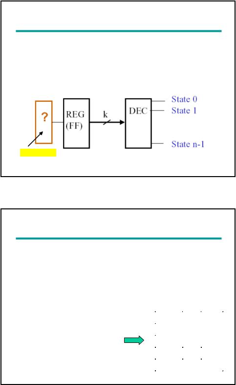
(2)Sequencer (sequence register) and Decoder
Use a register to represent the states and a decoder to generate an output signal corresponding to each state
Use the State Table to find the input logic
Input Logic
17
Multiplier Example: Sequencer and Decoder
Design - Specification
Define:
•States: IDLE, MUL0, MUL1
•Input Signals: G, Z, Q0 (Q0 affects outputs, not next state)
•Output Signals: Initialize, Load, Shift_Dec, Clear_C
•State Transition Diagram (Use Sequencing ASM)
•Output Function: Use Control Signal Table
•Decide on type of flip-flops to use
Find:
•State Assignments
•Use two state bits to encode the three states IDLE, MUL0, and MUL1.
State |
M1 |
M0 |
|
|
|
IDLE |
0 |
0 |
|
|
|
MUL0 |
0 |
1 |
|
|
|
MUL1 |
1 |
0 |
|
|
|
Unused |
1 |
1 |
|
|
|
18
9

Multiplier Example: Sequencer and Decoder
Design - Formulation
Assuming that state variables M1 and M0 are decoded into states, the next state part of the State Table is:
Current State |
Input |
Next State |
||
|
G Z |
M1 M0 |
||
|
|
|
|
|
IDLE |
0 |
0 |
0 |
0 |
IDLE |
0 |
1 |
0 |
0 |
IDLE |
1 |
0 |
0 |
1 |
IDLE |
1 |
1 |
0 |
1 |
MUL0 |
0 |
0 |
1 |
0 |
MUL0 |
0 |
1 |
1 |
0 |
MUL0 |
1 |
0 |
1 |
0 |
MUL0 |
1 |
1 |
1 |
0 |
Current State |
Input |
Next State |
||
|
G Z |
M1 M0 |
||
|
|
|
|
|
MUL1 |
0 |
0 |
0 |
1 |
MUL1 |
0 |
1 |
0 |
0 |
MUL1 |
1 |
0 |
0 |
1 |
MUL1 |
1 |
1 |
0 |
0 |
Unused |
0 |
0 |
d |
d |
Unused |
0 |
1 |
d |
d |
Unused |
1 |
0 |
d |
d |
Unused |
1 |
1 |
d |
d |
19
State Table with Decoder Outputs
20
10