

AS3400_10_30_Datasheet_EN_v4 (2) — копия
.pdfA S 3 4 0 0 / 1 0 / 3 0
L o w P o w e r A m b i e n t N o i s e - C a n c e l l i n g S p e a k e r D r i v e r
1 General Description
The AS3400/10/30 are speaker driver with Ambient Noise Cancelling function for headsets, headphones or ear pieces. It is intended to improve quality of e.g. music listening, a phone conversation etc. by reducing background ambient noise.
The fully analog implementation allows the lowest power consumption, lowest system BOM cost and most natural received voice enhancement otherwise difficult to achieve with DSP implementations. The device is designed to be easily applied to existing architectures.
An internal OTP-ROM can be optionally used to store the microphones gain calibration settings.
The AS3400/10/30 can be used in different configurations for best trade-off of noise cancellation, required filtering functions and mechanical designs.
The simpler feed-forward topology is used to effectively reduce low frequency background noise. The feed-back topology with either 1 or 2 filtering stages can be used to reduce noise for a larger frequency range, and to even implement transfer functions like speaker equalization, Baxandall equalization, high/low shelving filter and to set a predefined loop bandwidth.
The filter loop is optimized by the user for specific headset electrical and mechanical designs by dimensioning simple R, C components.
Most headset implementations will make use of a single noise detecting microphone. Two microphones could be used to allow for increased flexibility of their location in the headset mechanical design. Using the bridged mode allows to even drive high impedance headsets.
2 Key Features
Microphone Input
128 gain steps @ 0.375dB and MUTE with AGC
Differential, low noise microphone amplifier
Single ended or differential mode
Improved supply for electret microphone
MIC gain OTP programmable
High Efficiency Headphone Amplifier
2x34mW, 0.1% THD @ 16Ω, 1.5V supply, 100dB SNR
Bridged mode for e.g. 300Ω loads
Click and pop less start-up and mode switching
Line Input
Volume control via serial interface or volume pin
64 steps @ 0.75dB and MUTE, pop-free gain setting
Single ended stereo or mono differential mode
ANC processing
Feed-forward cancellation
Feed-back cancellation with filter loop transfer function definable via simple RC components
Simple in production SW calibration
12-30dB noise reduction (headset dependent)
10-2000Hz wide frequency active noise attenuation (headset dependent)
Monitor Function
For assisted hearing, i.e. to monitor announcements
Fixed (OTP prog.) ambient sound amplification to compensate headphone passive attenuation
Volume controlled ambient sound amplification mixed with fixed (OTP prog.) attenuation of LineIn
Incremental Functions
ANC with or without music on the receiving path
Improved dynamic range playback
OTP ROM for automatic trimming during production (4 times programmable)
Performance Parameter
5/3.8mA @ 1.5V stereo/mono ANC; <1µA quiescent
Extended PSRR for 217Hz
Interfaces
2-wire serial control mode & volume inputs
Calibration via Line-In or 2-wire serial interface (patent pending)
Single cell or fixed 1.0-1.8V supply with internal CP
Package
AS3400, AS3410 QFN24 [4x4mm] 0.5mm pitch
AS3430 QFN32 [5.x5mm] 0.5mm pitch
3 Applications
The devices are ideal for Ear pieces, Headsets, Hands-Free Kits, Mobile Phones, and Voice Communicating Devices.
www.ams.com/ANC |
Revision 1.10 |
1 - 53 |
AS3400/10/30
Data Sheet - A p p l i c a t i o n s
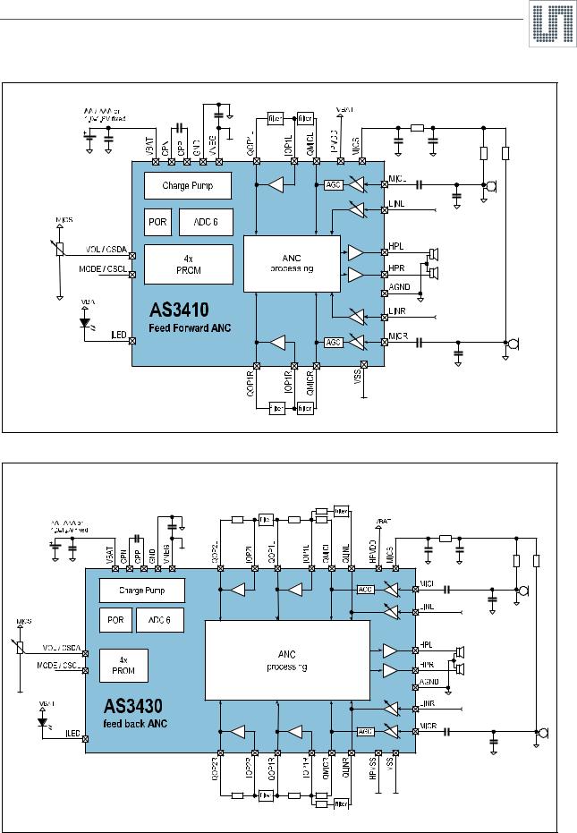
Figure 1. AS3410 Feed Forward ANC Block Diagram
Figure 2. AS3430 Feed-Back Block Diagram
www.ams.com/ANC |
Revision 1.10 |
2 - 53 |

AS3400/10/30
Data Sheet - A p p l i c a t i o n s
Figure 3. AS3400 Feed-Back Block Diagram
Figure 4. AS3400 Feed Forward Block Diagram
www.ams.com/ANC |
Revision 1.10 |
3 - 53 |

AS3400/10/30
Data Sheet - C o n t e n t s
Contents
1 |
General Description .................................................................................................................................................................. |
1 |
||
2 |
Key Features ............................................................................................................................................................................ |
1 |
||
3 |
Applications |
.............................................................................................................................................................................. |
1 |
|
4 |
Pin Assignments ....................................................................................................................................................................... |
5 |
||
|
4.1 |
Pin Descriptions ................................................................................................................................................................................... |
6 |
|
5 |
Absolute Maximum Ratings ...................................................................................................................................................... |
8 |
||
6 |
Electrical Characteristics .......................................................................................................................................................... |
9 |
||
7 |
Typical Operating Characteristics ............................................................................................................................................ |
11 |
||
8 |
Detailed Description ............................................................................................................................................................... |
15 |
||
|
8.1 |
Audio Line Input ................................................................................................................................................................................. |
15 |
|
|
|
8.1.1 |
Gain Stage ................................................................................................................................................................................. |
15 |
|
|
8.1.2 |
Parameter .................................................................................................................................................................................. |
15 |
|
8.2 |
Microphone Input ............................................................................................................................................................................... |
16 |
|
|
|
8.2.1 |
Gain Stage & Limiter .................................................................................................................................................................. |
16 |
|
|
8.2.2 |
Supply ........................................................................................................................................................................................ |
16 |
|
|
8.2.3 |
Parameter .................................................................................................................................................................................. |
17 |
|
8.3 |
Headphone Output ............................................................................................................................................................................. |
18 |
|
|
|
8.3.1 |
Input Multiplexer ........................................................................................................................................................................ |
18 |
|
|
8.3.2 |
No-Pop Function ........................................................................................................................................................................ |
18 |
|
|
8.3.3 |
No-Clip Function ........................................................................................................................................................................ |
18 |
|
|
8.3.4 |
Over-Current Protection ............................................................................................................................................................. |
19 |
|
|
8.3.5 |
Parameter .................................................................................................................................................................................. |
19 |
|
8.4 |
Operational Amplifier .......................................................................................................................................................................... |
19 |
|
|
|
8.4.1 |
Parameter .................................................................................................................................................................................. |
20 |
|
8.5 |
SYSTEM ............................................................................................................................................................................................ |
21 |
|
|
|
8.5.1 Power Up/Down Conditions ....................................................................................................................................................... |
21 |
|
|
|
8.5.2 |
Start-up Sequence ..................................................................................................................................................................... |
21 |
|
|
8.5.3 |
Mode Switching ......................................................................................................................................................................... |
22 |
|
|
8.5.4 |
Status Indication ........................................................................................................................................................................ |
23 |
|
8.6 |
VNEG Charge Pump .......................................................................................................................................................................... |
23 |
|
|
|
8.6.1 |
Parameter .................................................................................................................................................................................. |
23 |
|
8.7 |
OTP Memory & Internal Registers ..................................................................................................................................................... |
23 |
|
|
|
8.7.1 |
Register & OTP Memory Configuration ..................................................................................................................................... |
23 |
|
|
8.7.2 OTP Fuse Burning ..................................................................................................................................................................... |
24 |
|
|
8.8 |
2-Wire-Serial Control Interface ........................................................................................................................................................... |
25 |
|
|
|
8.8.1 |
Protocol ...................................................................................................................................................................................... |
25 |
|
|
8.8.2 |
Parameter .................................................................................................................................................................................. |
28 |
9 |
Register Description ............................................................................................................................................................... |
29 |
||
10 |
Application Information ......................................................................................................................................................... |
44 |
||
11 Package Drawings and Marking ........................................................................................................................................... |
49 |
|||
Ordering Information .................................................................................................................................................................... |
53 |
|||
www.ams.com/ANC |
Revision 1.10 |
4 - 53 |

AS3400/10/30
Data Sheet - P i n A s s i g n m e n t s
4 Pin Assignments
Note: Pin assignment may change in preliminary data sheets.
Figure 5. Pin Assignments (Top View)
CAUTION: Exposed pad must be connect to VNEG or left unconnected. Exposed pad must NOT be connected to GND or AGND!
www.ams.com/ANC |
Revision 1.10 |
5 - 53 |

AS3400/10/30
Data Sheet - P i n A s s i g n m e n t s
4.1 Pin Descriptions
Note: Pin description may change in preliminary data sheets.
Table 1. Pin Description for AS3400 AS3410 AS3430
Pin Name |
|
Pin Number |
|
Type |
Description |
|
|
|
|
||||
AS3400 |
AS3410 |
AS3430 |
||||
|
|
|
||||
IOP1L |
- |
24 |
1 |
ANA IN |
Filter OpAmp1 Input Left Channel |
|
|
|
|
|
|
|
|
QLINL |
- |
- |
2 |
ANA OUT |
Line In GainStage Output Left Channel |
|
|
|
|
|
|
|
|
QMICL |
24 |
1 |
3 |
ANA OUT |
MIC GainStage Output Right Channel |
|
|
|
|
|
|
|
|
AGND |
1 |
2 |
4 |
ANA IN |
Analog Reference |
|
|
|
|
|
|
|
|
|
|
|
|
ANA IN |
Line In Left Channel |
|
LINL |
2 |
3 |
5 |
During Appl Trim Mode Write – CSDA |
||
DIG IN |
||||||
|
|
|
|
During Appl Trim Mode Burn – VNEG |
||
|
|
|
|
|
||
|
|
|
|
|
|
|
|
|
|
|
ANA IN |
LineIn Right Channel |
|
LINR |
3 |
4 |
6 |
During Appl Trim Mode Write – CSCL |
||
DIG IO |
||||||
|
|
|
|
During Appl Trim Mode Burn – Clock |
||
|
|
|
|
|
||
|
|
|
|
|
|
|
VOL_CSDA |
4 |
5 |
7 |
MIXED IO |
Serial Interface Data |
|
ADC Input for volume regulation |
||||||
|
|
|
|
|
||
|
|
|
|
|
|
|
MODE_CSCL |
5 |
6 |
8 |
DIG IN |
Mode Pin (PowerUp/Dn, Monitor) |
|
Serial Interface Clock |
||||||
|
|
|
|
|
||
|
|
|
|
|
|
|
MICL |
6 |
7 |
9 |
ANA IN |
Microphone In Left Channel |
|
|
|
|
|
|
|
|
ILED |
- |
8 |
10 |
ANA OUT |
Current Output for on-indication LED |
|
|
|
|
|
|
|
|
MICS |
7 |
9 |
11 |
ANA OUT |
Microphone Supply |
|
|
|
|
|
|
|
|
MICR |
8 |
10 |
12 |
ANA IN |
Microphone Input Right Channel |
|
|
|
|
|
|
|
|
QMICR |
9 |
11 |
13 |
ANA OUT |
MIC GainStage Output Right Channel |
|
|
|
|
|
|
|
|
QLINR |
10 |
- |
14 |
ANA OUT |
Line In GainStage Output Right Channel |
|
|
|
|
|
|
|
|
IOP1R |
11 |
12 |
15 |
ANA IN |
FilterOpAmp1 Input Right Channel |
|
|
|
|
|
|
|
|
QOP1R |
12 |
13 |
16 |
ANA IN |
Filter OpAmp1 Output Right Channel |
|
|
|
|
|
|
|
|
IOP2R |
13 |
- |
17 |
ANA IN |
Filter OpAmp2 Input Right Channel |
|
|
|
|
|
|
|
|
QOP2R |
14 |
- |
18 |
ANA OUT |
Filter OpAmp2 Output Right Channel |
|
|
|
|
|
|
|
|
VSS |
15 |
14 |
19 |
SUP IN |
Core and Periphery Circuit VSS Supply |
|
|
|
|
|
|
|
|
HPL |
16 |
15 |
20 |
ANA OUT |
Headphone Output Left Channel |
|
|
|
|
|
|
|
|
HPVSS |
- |
- |
21 |
SUP IN |
Headphone VSS Supply |
|
|
|
|
|
|
|
|
HPR |
17 |
16 |
22 |
ANA OUT |
Headphone Output Right Channel |
|
|
|
|
|
|
|
|
HPVDD |
18 |
17 |
23 |
SUP IN |
Headphone VDD Supply |
|
|
|
|
|
|
|
|
VBAT |
19 |
18 |
24 |
SUP IN |
VNEG ChargePump Positive Supply |
|
|
|
|
|
|
|
|
n.c. |
- |
- |
25 |
- |
|
|
|
|
|
|
|
|
|
CPP |
20 |
19 |
26 |
ANA OUT |
VNEG ChargePump Flying Capacitor Positive Terminal |
|
|
|
|
|
|
|
|
GND |
21 |
20 |
27 |
GND |
VNEG ChargePump Negative Supply |
|
|
|
|
|
|
|
|
CPN |
22 |
21 |
28 |
ANA OUT |
VNEG ChargePump Flying Capacitor Negative Terminal |
|
|
|
|
|
|
|
|
VNEG |
23 |
22 |
29 |
SUP IO |
VNEG ChargePump Output |
|
|
|
|
|
|
|
www.ams.com/ANC |
Revision 1.10 |
6 - 53 |

AS3400/10/30
Data Sheet - P i n A s s i g n m e n t s
Table 1. Pin Description for AS3400 AS3410 AS3430
Pin Name |
|
Pin Number |
|
Type |
Description |
|
|
|
|
||||
AS3400 |
AS3410 |
AS3430 |
||||
|
|
|
||||
QOP2L |
- |
- |
30 |
ANA OUT |
Filter OpAmp2 Output Left Channel |
|
|
|
|
|
|
|
|
IOP2L |
- |
- |
31 |
ANA IN |
Filter OpAmp2 Input Left Channel |
|
|
|
|
|
|
|
|
QOP1L |
- |
23 |
32 |
ANA OUT |
Filter OpAmp1 Output Right Channel |
|
|
|
|
|
|
|
|
|
25 |
25 |
33 |
|
Exposed Pad: connect to VNEG or leave it unconnected |
|
|
|
|
|
|
|
www.ams.com/ANC |
Revision 1.10 |
7 - 53 |

AS3400/10/30
Data Sheet - A b s o l u t e M a x i m u m R a t i n g s
5 Absolute Maximum Ratings
Stresses beyond those listed in Table 2 may cause permanent damage to the device. These are stress ratings only, and functional operation of the device at these or any other conditions beyond those indicated in Electrical Characteristics on page 9 is not implied. Exposure to absolute maximum rating conditions for extended periods may affect device reliability. The device should be operated under recommended operating conditions.
Table 2. Absolute Maximum Ratings
Parameter |
|
Min |
Max |
Units |
Comments |
Reference Ground |
|
|
|
|
Defined as in GND |
|
|
|
|
|
|
Supply terminals |
|
-0.5 |
2.0 |
V |
Applicable for pin VBAT, HPVDD |
|
|
|
|
|
|
Ground terminals |
|
-0.5 |
0.5 |
V |
Applicable for pins AGND |
|
|
|
|
|
|
Negative terminals |
|
-2.0 |
0.5 |
V |
Applicable for pins VNEG, VSS, HPVSS |
|
|
|
|
|
|
Voltage difference at VSS terminals |
|
-0.5 |
0.5 |
V |
Applicable for pins VSS, HPVSS |
|
|
|
|
|
|
Pins with protection to VBAT |
|
VNEG |
5.0 |
V |
Applicable for pins CPP, CPN |
|
-0.5 |
VBAT+0.5 |
|||
|
|
|
|
||
|
|
|
|
|
|
Pins with protection to HPVDD |
|
VSS |
5.0 |
V |
Applicable for pins LINL/R, MICL/R, ILED, HPR, |
|
-0.5 |
HPVDD+0.5 |
HPL, QMICL/R, QLINL/R, IOPx, QOPx |
||
|
|
|
|||
|
|
|
|
|
|
other pins |
|
VSS |
5 |
|
Applicable for pins MICS, VOL_CSDA, |
|
-0.5 |
|
MODE_CSCL |
||
|
|
|
|
||
|
|
|
|
|
|
Input Current (latch-up immunity) |
|
-100 |
100 |
mA |
Norm: JEDEC 17 |
|
|
|
|
|
|
Continuous Power Dissipation (TA = +70ºC) |
|
|
|
|
|
|
|
|
|
|
|
Continuous Power Dissipation |
|
- |
200 |
mW |
PT1 for QFN16/24/32 package |
Electrostatic Discharge |
|
|
|
|
|
|
|
|
|
|
|
Electrostatic Discharge HBM |
|
|
+/-2 |
kV |
Norm: JEDEC JESD22-A114C |
|
|
|
|
|
|
Temperature Ranges and Storage Conditions |
|
|
|
|
|
|
|
|
|
|
|
Junction Temperature |
|
|
+110 |
ºC |
|
|
|
|
|
|
|
Storage Temperature Range |
|
-55 |
+125 |
ºC |
|
|
|
|
|
|
|
Humidity non-condensing |
|
5 |
85 |
% |
|
|
|
|
|
|
|
Moisture Sensitive Level |
|
|
3 |
|
Represents a max. floor life time of 168h |
|
|
|
|
|
|
|
|
|
|
|
The reflow peak soldering temperature (body |
|
|
|
|
|
temperature) specified is in accordance with IPC/ |
Package Body Temperature |
|
|
260 |
ºC |
JEDEC J-STD-020“Moisture/Reflow Sensitivity |
|
|
|
|
|
Classification for Non-Hermetic Solid State |
|
|
|
|
|
Surface Mount Devices”. |
|
|
|
|
|
|
1. Depending on actual PCB layout and PCB used |
|
|
|
|
|
www.ams.com/ANC |
Revision 1.10 |
8 - 53 |

AS3400/10/30
Data Sheet - E l e c t r i c a l C h a r a c t e r i s t i c s
6 Electrical Characteristics
VBAT = 1.0V to 1.8V, TA = -20ºC to +85ºC. Typical values are at VBAT = 1.5V, TA = +25ºC, unless otherwise specified. All limits are guaranteed. The parameters with min and max values are guaranteed with production tests or SQC (Statistical Quality Control) methods.
Table 3. Electrical Characteristics
Symbol |
Parameter |
Condition |
Min |
Max |
Unit |
|
TA |
Ambient Temperature Range |
|
-20 |
+85 |
°C |
|
|
|
|
|
|
|
|
Supply Voltages |
|
|
|
|
||
|
|
|
|
|
|
|
GND |
Reference Ground |
|
0 |
0 |
V |
|
|
|
|
|
|
|
|
VBAT, |
Battery Supply Voltage |
normal operation with MODE pin high |
1.0 |
1.8 |
V |
|
|
|
|
|
|||
HPVDD |
Two wire interface operation |
1.4 |
1.8 |
V |
||
|
||||||
|
|
|||||
|
|
|
|
|
|
|
VNEG |
ChargePump Voltage |
|
-1.8 |
-0.7 |
V |
|
|
|
|
|
|
|
|
VSS |
Analog neg. Supply Voltages |
|
-1.8 |
-0.7 |
V |
|
HPVSS, VSS, VNEG |
|
|||||
|
|
|
|
|
||
|
|
|
|
|
|
|
|
Difference of Ground Supplies |
To achieve good performance, the negative |
|
|
|
|
VDELTA- |
supply terminals should be connected to low |
-0.1 |
0.1 |
V |
||
GND, AGND |
||||||
|
impedance ground plane. |
|
|
|
||
|
|
|
|
|
||
|
|
|
|
|
|
|
VDELTA-- |
Difference of Negative Supplies |
Charge pump output or external supply |
-0.1 |
0.1 |
V |
|
VSS, VNEG, HPVSS |
||||||
|
|
|
|
|
||
|
|
|
|
|
|
|
VDELTA+ |
Difference of Positive Supplies |
VBAT-HPVDD |
-0.25 |
0.25 |
V |
|
Other pins |
|
|
|
|
|
|
|
|
|
|
|
|
|
VMICS |
Microphone Supply Voltage |
MICS |
0 |
3.6 |
V |
|
VHPVDD |
Pins with diode to HPVDD |
MICL/R, ILED, HPR, HPL, QMICL/R, QLINL/ |
VSS |
3.6 |
V |
|
R, IOPx, QOPx |
||||||
|
|
|
|
|
||
|
|
|
|
|
|
|
VVBAT |
Pins with diode to VBAT |
CPP, CPN |
VNEG |
VBAT |
V |
|
VCONTROL |
Control Pins |
MODE_CSCL, VOL_CSDA |
VSS |
3.7 |
V |
|
|
|
|
|
|
||
|
|
|
|
|
|
|
VTRIM |
Line Input & Application Trim Pins |
LINL, LINR |
VNEG -0.5 |
HPVDD +0.5 |
V |
|
or -1.8 |
or 1.8 |
|||||
|
|
|
|
|||
|
|
|
|
|
|
|
Symbol |
Parameter |
Condition |
Min |
Typ |
Max |
Unit |
Ileak |
Leakage current |
VBAT<0.8V |
|
|
20 |
µA |
|
|
|
|
|
||
VBAT<0.6V |
|
|
10 |
µA |
||
|
|
|
|
|||
|
|
|
|
|
|
|
Block Power Requirements @ 1.5V VBAT |
|
|
|
|
|
|
|
|
|
|
|
|
|
IOFF |
Off mode current |
MODE pin low, device switched off |
|
1 |
|
µA |
ISYS |
Reference supply current |
Bias generation, oscillator, ILED current sink, |
|
0.25 |
|
mA |
ADC6 |
|
|
||||
|
|
|
|
|
|
|
|
|
|
|
|
|
|
ILIN |
LineIn gain stage current |
no signal, stereo |
|
0.64 |
|
mA |
IMIC |
Mic gain stage current |
no signal, stereo |
|
2.10 |
|
mA |
IHP |
Headphone stage current |
no signal |
|
1.70 |
|
mA |
IVNEG |
VNEG charge pump current |
no load |
|
0.25 |
|
mA |
IMICS |
MICS charge pump current |
no load |
|
0.06 |
|
mA |
IMIN |
Minimal supply current |
Sum of all above blocks |
|
5.00 |
|
mA |
www.ams.com/ANC |
Revision 1.10 |
9 - 53 |

AS3400/10/30
Data Sheet - E l e c t r i c a l C h a r a c t e r i s t i c s
Symbol |
Parameter |
Condition |
Min |
Typ |
Max |
Unit |
IOP1 |
OP1 supply current |
no load |
|
0.64 |
|
mA |
IOP2 |
OP2 supply current |
no load |
|
0.64 |
|
mA |
IILED |
ILED current sink current |
100% duty cycle |
|
2.50 |
|
mA |
IMICB |
Microphone bias current |
200µA per microphone via charge pump |
|
1.30 |
|
mA |
www.ams.com/ANC |
Revision 1.10 |
10 - 53 |