

Маршрут проектирования систем с применением ПЛИС
Программный пакет: Integrated Software Environment (ISE)
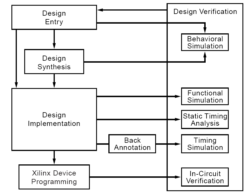
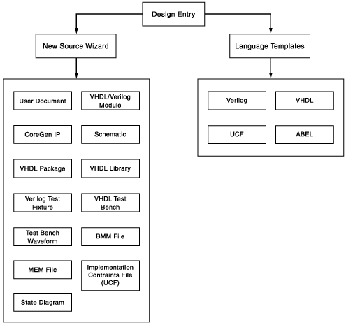
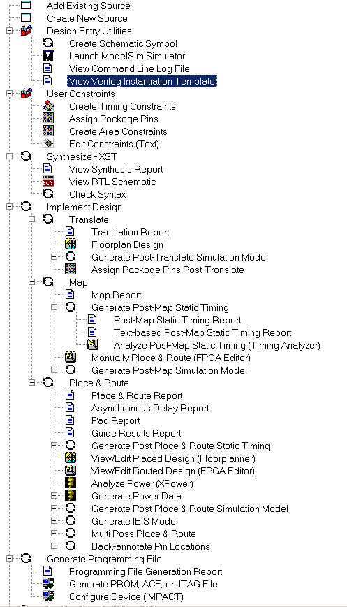
Design Entry
-
Create a new project, or open a current project.
-
Create and add files to your project.
-
Create an implementation constraints (UCF) file (optional).
-
Assign constraints such as timing constraints, pin assignments, and area constraints.
Design Entry (2)
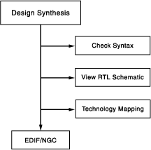
Design Synthesis
-
Set synthesis and/or implementation properties.
-
Simulate the behavior of your design.
Simulation is commonly run after translate or synthesis (behavioral), after implementation (functional) and after place and route (timing). Other simulation points are after the mapping process.
-
Run the Synthesis Process.
-
Simulate the function of your design.
A MEM file is a memory file used as input for Block RAM input.
A BMM file is a Block RAM Memory Map file.
The UCF (User Constraints File) is an ASCII file specifying constraints on the logical design.
EDIF is the Electronic Data Interchange Format, an industry standard file format for specifying a design netlist.
It is generated by a third party design-entry tool. In the Xilinx Project Navigator flow, EDIF is the standard input format.
The NGC file is a netlist that contains both logical design data and constraints. This file replaces both EDIF and NCF files when the XST synthesis tool is used.
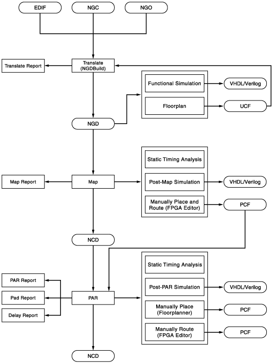
The Netlister Launcher, which is part of NGDBuild, translates an EDIF or XNF netlist to an NGO file.
NGDBuild uses this NGO file to create an NGD file.
A Native Generic Database (NGD) file that describes the logical design reduced to Xilinx primitives.
A Native Circuit Description (NCD) file represents the physical circuit description of the input design as it applies to a specific device.
Physical Constraints File (PCF). This file contains the physical constraints that are derived from the logical constraints after mapping. Any changes in constraints in the FPGA Editor are also written to the PCF.
Place and route tool (PAR). PAR is a program for mapping, placing, and routing an FPGA design.
The process is called design implementation.
Mapping (MAP) is the process of assigning a design’s logic elements to the specific physical elements that actually implement logic functions in a device.
Design Implementation
-
Implement your design.
Your design will be implemented (Translate, Map, Place & Route).
-
Review reports for translate, map, place & route, and timing results.
-
Change properties, constraints, and source as necessary, then re-synthesize and re-implement your design. Repeat until design requirements are met.
-
View the placed design in Floorplanner. You can manually place and group logic prior to Mapping with Floorplanner (optional).
-
View the placed and routed design in FPGA Editor. You can manually route sections of the design in FPGA Editor (optional).
-
Set up multiple place and route runs on your design. The tools will identify the best results and keep as many as you specify (optional).
Design Verification
-
Create a programming file (.BIT) to program your FPGA.
-
Generate a PROM, ACE, or JTAG file for debugging or to download to your device.
-
Use iMPACT to program the device with a programming cable.
The Generate Programming File process runs BitGen, the Xilinx bitstream generation program, to produce a bitstream (.BIT) or (.ISC) file for Xilinx device configuration.
A bitstream (.bit) is a stream of data that contains location information for logic on a device, that is, the placement of Configurable Logic Blocks (CLBs), Input/Output Blocks (IOBs), (TBUFs), pins, and routing elements. The bitstream also includes empty placeholders that are filled with the logical states sent by the device during a readback. Only the memory elements, such as flip-flops, RAMs, and CLB outputs, are mapped to these placeholders, because their contents are likely to change from one state to another. When downloaded to a device, a bitstream configures the logic of a device and programs the device so that the states of that device can be read back. A bitstream file has a .bit extension.
Работа с программами:
-
Project Navigator
-
Core generator
-
Floorplaner
-
FPGA Editor
-
PACE
-
State CAD
-
XPower
-
Constraints Editor
-
Chip Viewer
-
Chip Scope
-
Architecture Wizard
-
iMPACT
-
Моделирование ModelSim SE 5.6b.
XPower enables you to interactively and automatically analyze power consumption for Xilinx FPGA and CPLD devices.
Pinout and Area Constraints Editor (PACE) is an interactive graphical application that you can use as follows:
-
To view and edit location constraints for I/Os and global logic
-
To view and create area constraints for hierarchical symbols in your design
-
To determine connectivity and resource requirements of your design
-
To determine resource layout of your target device
-
To determine how your design maps onto the device via location and area constraints (area constraints are for FPGA only)
The ChipViewer tool provides a graphical view of the fitting report. With this tool you can examine inputs and outputs, macrocell details, equations, and pin assignments. The ChipViewer will also access the Timing Analyzer Report.
iMPACT enables you to configure your PLD designs using Boundary-Scan, Slave Serial, and Select Map configuration modes, as well as the MultiPRO Desktop Programmer. You can also generate programming files using iMPACT’s System ACE, PROM Formatter, SVF, and STAPL file generation modes. iMPACT is provided with the Xilinx ISE software.
Design Entry
-
ISE Text Editor - The ISE Text Editor is provided in ISE for entering design code and viewing reports.
-
Schematic Editor - The Engineering Capture System (ECS) is a graphical user interface (GUI) that allows you to create, view, and edit schematics and symbols for the Design Entry step of the Xilinx® design flow.
-
CORE Generator - The CORE Generator System is a design tool that delivers parameterized cores optimized for Xilinx FPGAs ranging in complexity from simple arithmetic operators such as adders, to system-level building blocks such as filters, transforms, FIFOs, and memories.
-
Constraints Editor - The Constraints Editor allows you to create and modify the most commonly used timing constraints.
-
PACE - The Pinout and Area Constraints Editor (PACE) allows you to view and edit I/O, Global logic, and Area Group constraints.
-
StateCAD State Machine Editor - StateCAD allows you to specify states, transitions, and actions in a graphical editor. The state machine will be created in HDL.
Synthesis
-
XST - Xilinx Synthesis Technology.
-
Integration with LeonardoSpectrum from Mentor Graphics, Inc.
-
Integration with Synplify from Synplicity, Inc.
Simulation
-
HDL Bencher test bench waveform - The HDL Bencher tool automates creation of test benches and test fixtures using a graphical waveform editor.
-
Integration with ModelSim Simulator from Model Technology, Inc.
Implementation
-
Translate - The Translate process runs NGDBuild to merge all of the input netlists as well as design constraint information into a Xilinx database file.
-
Map - The Map program maps a logical design to a Xilinx FPGA.
-
Place and Route (PAR) - The PAR program accepts the mapped design, places and routes the FPGA, and produces output for the bitstream generator.
-
Floorplanner - The Floorplanner allows you to view a graphical representation of the FPGA, and to view and modify the placed design.
-
FPGA Editor - The FPGA Editor allows you view and modify the physical implementation, including routing.
-
Timing Analyzer - The Timing Analyzer provides a way to perform static timing analysis on FPGA and CPLD designs. With Timing Analyzer, analysis can be performed immediately after mapping, placing or routing an FPGA design, and after fitting and routing a CPLD design.
-
Fit (CPLD only) - The CPLDFit process maps a netlist(s) into specified devices and creates the JEDEC programming file.
-
ChipViewer (CPLD only) - The ChipViewer tool provides a graphical view of the inputs and outputs, macrocell details, equations, and pin assignments.
Device Download and Program File Formatting
-
BitGen - The BitGen program receives the placed and routed design and produces a bitstream for Xilinx device configuration.
-
iMPACT - The iMPACT tool generates various programming file formats, and subsequently allows you to configure your device.
-
XPower - XPower enables you to interactively and automatically analyze power consumption for Xilinx FPGA and CPLD devices.
-
Integration with ChipScope Pro.