

Cadence / DSD2 / Конспект -Введение в Cadence DSD2 / Конспект -Введение в Cadence DSD2 / Лекция2 / intro_tutorial
.pdfFig. 9. Properties of vpulse.
Step 9: Repeat step 5 – 6, but adding a gnd with properties in Fig. 10.
- 10 -
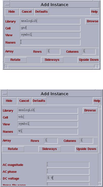
Fig. 10. Adding a gnd.
Step 10: Repeat step 5 – 6, but adding a vdc with properties in Fig. 11.
Fig. 11. Properties of vdc.
Step 11: In Composer-Schematic window, go to Add… Pin. Filling out the pop-up form as shown in Fig. 12. Then stamp it according to Fig. 13.
- 11 -
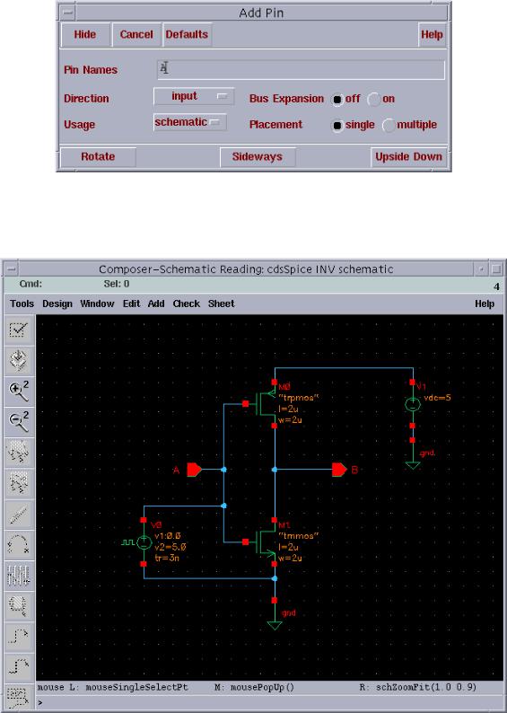
Fig. 12. Adding a pin.
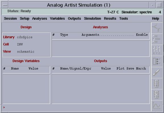
Step 12: In Composer-Schematic window, go to Add… Wire, connecting all the components according to Fig. 13.
Fig. 13. The completed INV schematic.
- 12 -
Step 13: In Composer-Schematic window, go to Design… Check and Save. Correcting all the errors in your schematic figure.
Step 14: In Composer-Schematic window, go to Tools… Analog Artist, an Analog Artist Simulation window appears as Fig. 14.
Fig. 14. Analog Artist Simulation window.
Step 15: In Analog Artist Simulation window, go to Setup… Model Libraries…, a
Model Library Setup window appears. Choosing the model path in your home directory by clicking Browse…, then click Add, as Fig. 15.
- 13 -
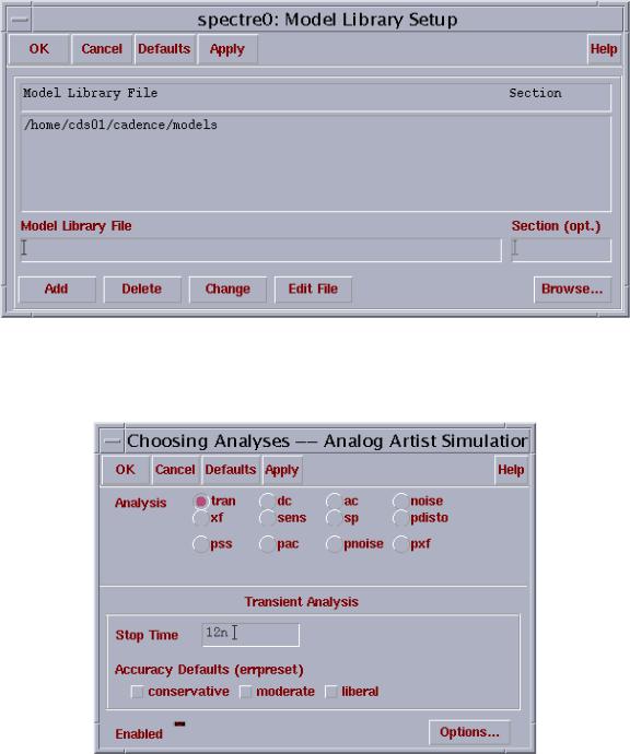
Fig. 15. Adding model path.
Step 16: In Analog Artist Simulation window, go to Analysis… Choose…, and fill out the form according to Fig. 16.
Fig. 16. Setting up transient analysis.
Step 17: In Analog Artist Simulation window, go to Outputs… To be Plotted… Select on Schematic. Then going back to the schematic window and selecting the wires attached to the pin A and B. Note, the wires should change the color, and the signals should be added in the outputs window, as Fig. 17.
- 14 -
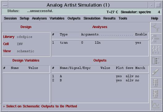
Fig. 17. Analog artist ready for a simulation.
Step 18: In Analog Artist Simulation window, go to Simulation… Run. The plot of the simulation should appear in a Waveform Window, like Fig. 18.
- 15 -
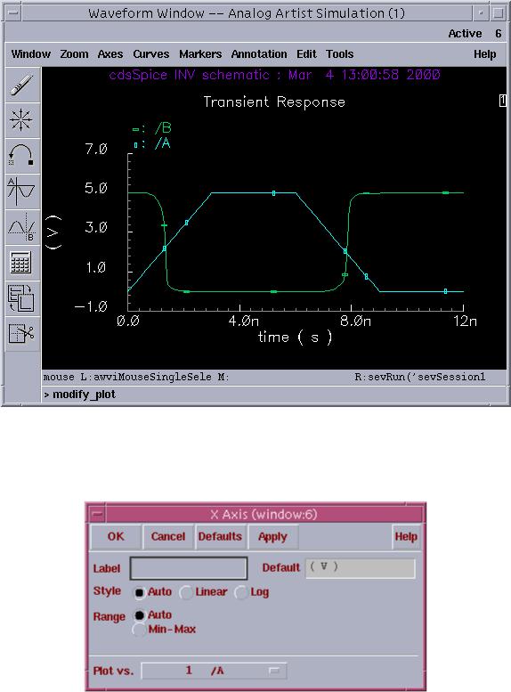
Fig. 18. INV simulation result.
Step 19: In the Waveform Window, go to Axes… Xaxis and change Plot vs independent variable to Plot vs 1/A, like Fig. 19. The final plot is like Fig. 20.
Fig. 19. Axis form.
- 16 -
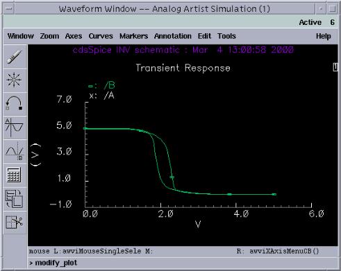
Fig. 20. Output voltage vs input voltage for a CMOS inverter.
Step 20: Go back to the schematic window, delete the vpulse and add a vsin according to Fig. 21.
- 17 -
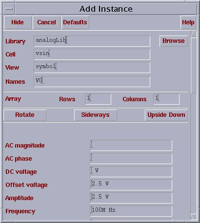
Fig. 21. Adding a sine wave input.
Step 21: Re-run the simulation, and your output is like Fig. 22.
- 18 -
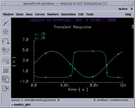
Fig. 22. Simulation result for a sine wave input.
Step 22: In Analog Artist Simulation window, go to Session… Save State…, then select OK.
Step 23: Exit the Analog Artist Simulation window, and exit the Composer-Schematic window.
Step 24: In the CIW window, go to File… Exit.
- 19 -