


Chapter 4
A PSO Approach in Optimal FACTS Selection with Harmonic Distortion Considerations
H.C. Leung and Dylan D.C. Lu
Additional information is available at the end of the chapter
http://dx.doi.org/10.5772/54555
1. Introduction
Static Var Compensator (SVC) has been commonly used to provide reactive power compensation in distribution systems [1]. The SVC placement problem is a well-researched topic. Earlier approaches differ in problem formulation and the solution methods. In some approaches, the objective function is considered as an unconstrained maximization of savings due to energy loss reduction and peak power loss reduction against the SVC cost. Others formulated the problem with some variations of the above objective function. Some have also formulated the problem as constrained optimization and included voltage constraints into consideration.
In today’s power system, there is trend to use nonlinear loads such as energy-efficient fluorescent lamps and solid-state devices. The SVCs sizing and allocation [2-4] should be properly considered, if else they can amplify harmonic currents and voltages due to possible resonance at one or several harmonic frequencies and switching actions of the power electronics converters connected. This condition could lead to potentially dangerous magnitudes of harmonic signals, additional stress on equipment insulation, increased SVC failure and interference with communication system.
SVC values are often assumed as continuous variables whose costs are considered as proportional to SVC size in past researches. Moreover, the cost of SVC is not linearly proportional to the size (MVAr). Hence, if the continuous variable approach is used to choose integral SVC size, the method may not result in an optimum solution and may even lead to undesirable harmonic resonance conditions.
Current harmonics are inevitable during the operation of thyristor controlled rectifiers, thus it is essential to have filters in a SVC system to eliminate the harmonics. The filter banks can not only absorb the risk harmonics, but also produce the capacitive reactive power. The SVC
62 An Update on Power Quality
uses close loop control system to regulate busbar voltage, reactive power exchange, power factor and three phase voltage balance.
This chapter describes a method based on Particle Swarm Optimisation (PSO) [5] to solve the optimal SVC allocation successfully. Particle Swarm Optimisation (PSO) method is a powerful optimization technique analogous to the natural genetic process in biology. Theoretically, this technique is a stochastic approach and it converges to the global optimum solution, provided that certain conditions are satisfied. This chapter considers a distribution system with 9 possible locations for SVCs and 27 different sizes of SVCs. A critical discussion using the example with result is discussed in this chapter.
2. Problem formulation
2.1. Operation principal of SVC
The Static Var Compensator (SVC) are composed of the capacitor banks/filter banks and aircore reactors connected in parallel. The air-core reactors are series connected to thyristors. The current of air-core reactors can be controlled by adjusting the fire angle of thyristors.
The SVC can be considered as a dynamic reactive power source. It can supply capacitive reactive power to the grid or consume the spare inductive reactive power from the grid. Normally, the system can receive the reactive power from a capacitor bank, and the spare part can be consumed by an air-core shunt reactor. As mentioned, the current in the air-core reactor is controlled by a thyristor valve. The valve controls the fundamental current by changing the fire angle, ensuring the voltage can be limited to an acceptable range at the injected node(for power system var compensation), or the sum of reactive power at the injected node is zero which means the power factor is equal to 1 (for load var compensation).
2.2. Assumptions
The optimal SVC placement problem [6] has many variables including the SVC size, SVC cost, locations and voltage constraints on the system. There are switchable SVCs and fixedtype SVCs in practice. However, considering all variables in a nonlinear fashion will make the placement problem very complicated. In order to simplify the analysis, the assumptions are as follows: 1) balanced conditions, 2) negligible line capacitance, 3) time-invariant loads and 4) harmonic generation is solely from the substation voltage supply.
2.3. Radial distribution system
Figure 1 clearly illustrates an m-bus radial distribution system where a general bus i contains a load and a shunt SVC. The harmonic currents introduced by the nonlinear loads are injected at each bus
At the power frequency, the bus voltages are found by solving the following mismatch equations:
A PSO Approach in Optimal FACTS Selection with Harmonic Distortion Considerations 63
0 |
|
|
1 |
|
2 |
|
|
|
|
|
|
i |
m-1 |
||||||||||||||||
|
|
|
y 10 1 |
|
|
|
|
y 11 2 |
|
|
|
. . . . . . |
|
|
|
|
|
. . . . . . |
|
|
|
|
y 1m 1 ,m |
||||||
|
|
|
|
|
|
|
|
|
|
|
|||||||||||||||||||
|
|
|
|
|
|
|
|
|
|
|
|
|
|
|
|
|
|
|
|
|
|
|
|
|
|
|
|
|
|
|
|
|
|
|
|
|
|
|
|
|
|
|
y c i |
|
|
|
P n i , Q n i |
|
|
|
|||||||||
|
|
|
|
|
P 1 , Q 1 |
|
|
|
|
||||||||||||||||||||
|
|
|
|
|
|
P 2 , Q 2 |
P l i , Q l i |
P m 1 , Q m 1 |
|||||||||||||||||||||
Figure 1. One-line diagram of the radial distribution feeder.
Pi |
|
V 1i |
2 |
m |
V |
1i V |
1jY1ij |
|
cos 1ij 1j |
1i |
i |
1,2,3 m |
|
|
Gii |
|
|||||||||
|
|
|
|
j 1 |
|
|
|
|
|
|
|
|
|
|
|
|
j i |
|
|
|
|
|
|
|
|
Qi |
|
V 1i |
2 |
|
|
m |
|
1i V 1jY1ij |
|
sin 1ij |
1j |
1i |
|||||||
|
Bii |
V |
|
||||||||||||||||
|
|
|
|
|
|
j 1 |
|
|
|
|
|
|
|
|
|
|
|
||
|
|
|
|
|
|
j i |
|
|
|
|
|
|
|
|
|
|
|||
where |
|
|
|
|
|
|
|
|
|
|
|
|
|
|
|
|
|
||
|
|
|
|
|
|
|
|
|
|
|
|
Pi |
|
|
Pli Pni |
|
|
||
|
|
|
|
|
|
|
|
|
|
|
|
Qi |
|
|
Qli Qni |
|
|||
|
|
|
|
|
|
|
|
|
|
|
|
|
|
|
|
|
1 |
|
|
|
|
|
1 |
|
|
1 |
|
|
1 |
|
|
|
|
|
yij |
|
|
||
|
|
|
|
|
|
|
|
|
|
||||||||||
|
|
Yij |
|
|
Yij |
|
|
ij |
|
|
|
|
|
|
|
|
|
||
|
|
|
|
|
|
|
|
|
|
|
|
y1 |
y1 |
|
y1 |
||||
|
|
|
|
|
|
|
|
|
|
|
|
|
|||||||
|
|
|
|
|
|
|
|
|
|
|
|
|
i 1,i |
i 1,i |
|
ci |
|||
|
|
|
|
|
|
|
|
|
|
|
|
Yii |
|
|
Gii jBii |
|
|||
i 1,2,3 m
if |
i j |
if |
i j |
m
P m , Q m
(1)
(2)
(3)
(4)
(5)
(6)
2.4. Real power losses
At fundamental frequency, the real power losses in the transmission line between buses i and i+1 is:
P1 Ri,i 1 loss i,i 1
So, the total real losses is:
Ploss N
n 1
|
|
V 1i 1 V 1i |
|
Y1i,i 1 |
|
2 |
|
|
|
|
|||||
m 1 |
|
|
|
||||
Plossn |
i,i 1 |
||||||
i 0 |
|
|
|
||||
(7)
(8)
2.5. Objective function and constraints
The objective function of SVC placement is to reduce the power loss and keep bus voltages and total harmonic distortion (HDF) within prescribed limits with minimum cost. The constraints are voltage limits and maximum harmonic distortion factor, with the harmonics
64 An Update on Power Quality
taken into account. Following the above notation, the total annual cost function due to SVC placement and power loss is written as :
Minimize
f KlKpPloss |
m |
|
|
||||
QcjKcj |
(9) |
||||||
|
|
|
|
|
j 1 |
|
|
where j = 1,2,….m represents the SVC sizes |
|
|
|
||||
|
|
|
|
Qcj j * Ks |
|
(10) |
|
The objective function (1) is minimized subject to |
|
|
|
||||
V min |
|
V i |
|
V max |
i |
1,2,3 m |
(11) |
|
|
||||||
and |
|
|
|
||||
HDFi HDFmax |
i |
1,2,3 m |
(12) |
||||
According to IEEE Standard 519 [7] utility distribution buses should provide a voltage harmonic distortion level of less than 5% provided customers on the distribution feeder limit their load harmonic current injections to a prescribed level.
3. Proposed algorithm
3.1. Harmonic power flow [8]
At the higher frequencies, the entire power system is modelled as the combination of harmonic current sources and passive elements. Since the admittance of system components will vary with the harmonic order, the admittance matrix is modified for each harmonic order studied. If the skin effect is ignored, the resulting n-th harmonic frequency load admittance, shunt SVC admittance and feeder admittance are respectively given by:
Ylin |
|
|
Pli |
|
j |
|
Qli |
|
(13) |
||
|
|
|
2 |
|
|
||||||
V 1 |
n |
V 1 |
2 |
|
|||||||
|
|
|
|
|
|||||||
|
|
|
i |
|
|
|
i |
|
|
|
|
|
Ycin nY1ci |
|
|
|
(14) |
||||||
Yin,i 1 |
|
|
1 |
|
|
|
(15) |
||||
Ri,i 1 jnXi,i 1 |
|||||||||||
|
|
|
|
||||||||
The linear loads are composed of a resistance in parallel with a reactance [9]. The nonlinear loads are treated as harmonic current sources, so the injection harmonic current source introduced by the nonlinear load at bus i is derived as follows:
A PSO Approach in Optimal FACTS Selection with Harmonic Distortion Considerations 65
|
P |
jQ |
* |
|
||
1 |
|
ni |
|
ni |
|
(16) |
|
V 1 |
|
||||
Ii |
|
|
|
|
||
|
|
i |
|
|
|
|
|
Iin C n I |
1 |
|
(17) |
||
|
|
|
|
i |
|
|
In this study, C(n) is obtained by field test and Fourier analysis for all the customers along the distribution feeder. The harmonic voltages are found by solving the load flow equation (18), which is derived from the node equations.
YnV n In |
(18) |
At any bus i, the r.m.s. value of voltage is defined by
|
|
N |
n |
2 |
|
V i |
|
(19) |
|||
V i |
|||||
|
|
n 1 |
|
|
where N is an upper limit of the harmonic orders being considered and is required to be within an acceptable range. After solving the load flow for different harmonic orders, the harmonic distortion factor (HDF) [8] that is used to describe harmonic pollution is calculated as follows:
|
N |
|
n |
|
2 |
|
|
|
|
|
|
||||
|
|
|
|
|
|
|
|
HDFi % |
|
V i |
|
|
|
|
|
n 2 |
|
|
|
|
100% |
(20) |
|
|
|
|
|||||
V 1i |
|
|
|||||
|
|
|
|
|
|||
It is also required to be lower than the accepted maximum value.
3.2. Selection of optimal SVC location
The general case of optimal SVC locations can be selected for starting iteration. PSO calculates the optimal SVC sizes according to the optimal SVC locations. After the first time iteration, the solution of SVC locations and sizes will be recorded as old solution and add more locations to consideration. PSO is used to calculate a new solution. If the new solution is better than the old solution, the old solution will be replaced by the new solution. If else, the old solution is the best solution. Therefore, this project will continue to consider more locations until no more optimal solution, which is better than the previous solution. In this chapter, the selection of optimal SVC location is based on the following criteria: voltage, real power loss, load reactive power and harmonic distortion factor with equal weighting.
3.3. Solution algorithm
PSO is a search algorithm based on the mechanism of natural selection and genetics. It consists of a population of bit strings transformed by three genetic operations: 1) Selection

66 An Update on Power Quality
or reproduction, 2) Crossover, and 3) mutation. Each string is called chromosome and represents a possible solution. The algorithm starts from an initial population generated randomly. Using the genetic operations considering the fitness of a solution, which corresponds, to the objective function for the problem generates a new generation. The string’s fitness is usually the reciprocal of the string’s objective function in minimization problem. The fitness of solutions is improved through iterations of generations. For each chromosome population in the given generation, a Newton-Raphson load flow calculation is performed. When the algorithm converges, a group of solutions with better fitness is generated, and the optimal solution is obtained. The scheme of genetic operations, the structure of genetic string, its encode/decode technique and the fitness function are designed. The implementation of PSO components and the neighborhood searching are explained as follows.
4. Implementation of PSO
This section provides a brief introductory concept of PSO. If Xi = (xi1, xi2 ,…, xid) and Vi =(vi1, vi2
,…, vid) are the position vector and the velocity vector respectively in d dimensions search space, then according to a fitness function, where Pi=(pi1, pi2,…, pid) is the pbest vector and Pg=(pg1, pg2,…, pgd) is the gbest vector, i.e. the fittest particle of Pi, updating new positions and velocities for the next generation can be determined.
For each particle
Initialize particle
END
Do
For each particle Calculate fitness value
If the fitness value is better than the best fitness value (pbest), set current value as the new pbest
End
Choose the particle with the best fitness value of all the particles as the gbest
For each particle
Calculate particle velocity from equation (21) Update particle position from equation (22)
End
Perform mutation operation with pm
While maximum iteration is reached or minimum error condition is satisfied
Figure 2. The pseudo code of the PSO method
A PSO Approach in Optimal FACTS Selection with Harmonic Distortion Considerations 67
Vid t Vid t 1 C1 * rand1* Pid Xid t 1 C2 * rand2 * Pgd Xid t 1 |
(21) |
Xid t Xid t 1 Vid t |
(22) |
where Vid is the particle velocity, Xid is the current particle (solution). Pid and Pgd are defined as above. rand1 and rand2 are random numbers which is uniformly distributed between [0,1]. C1, C2 are constant values which is usually set to C1 = C2 = 2.0. These constants represent the weighting of the stochastic acceleration which pulls each particle towards the pbest and gbest position. ω is the inertia weight and it can be expressed as follows:
ω i f * |
itermax iter |
ωf |
(23) |
iter |
|||
|
max |
|
|
where i and f are the initial and final values of the inertia weight respectively. iter and itermax are the current iterations number and maximum allowed iterations number respectively.
The velocities of particles on each dimension are limited to a maximum velocity Vmax. If the sum of accelerations causes the velocity on that dimension to exceed the user-specified Vmax, the velocity on that dimension is limited to Vmax.
In this chapter, the parameters used for PSO are as follows:
Number of particles in the swarm, N = 30 (the typical range is 20 – 40)
Inertia weight, wi = 0.9, wf = 0.4
Acceleration factor, C1 and C2 = 2.0
Maximum allowed generation, itermax = 100
The maximum velocity of particles, Vmax =10% of search space
There are two stopping criteria in this chapter. Firstly, i(t is the number of iterations since the last change of the best solution is greater than a preset number. The PSO is terminated while maximum iteration is reached.
For the PSO, the constriction and inertia weight factors are introduced and (21) is improved as follows.
Vid t k Vid t 1 1 * rand1* Pid Xid t 1 2 * rand2 * Pgd Xid t 1 |
(24) |
||
k |
2 |
|
(25) |
2 1 2 1 2 2 4 1 2 |
|
||
|
|
|
|
|
|
|
|
where k is a constriction factor from the stability analysis which can ensure the convergence (i.e. avoid premature convergence) where + > 4 and kmax < 1 and is dynamically set as follows:

68 An Update on Power Quality
|
ω ωmax |
max min |
t |
(26) |
|
|
|||
|
|
tTotal |
|
|
where t and tTotal is the current iteration and total number of iteration respectively and |
|
|||
and |
is the upper and lower limit which are set 1.3 and 0.1 respectively. |
|
||
The advantage of the integration of mutation from GAs is to prevent stagnation as the mutation operation choose the particles in the swarm randomly and the particles can move to difference position. The particles will update the velocities and positions after mutation.
mutation xid xid |
, 1 r 0 |
(27) |
mutation xid xid |
, 1 r 0 |
(28) |
where xid is a randomly chosen element of the particle from the swarm, ω is randomly generated within the range [0, × (particle max – particle min)] (particle max and particle min are the upper and lower boundaries of each particle element respectively) and r is the random number in between 1 and -1
Implementation of an optimization problem is realized within the evolutionary process of a fitness function. The fitness function adopted is derived as equation (9). The objective function is to minimize f. It is composed of two parts; 1) the cost of the power loss in the transmission branch and 2) the cost of reactive power supply. Since PSO is applied to maximization problem, minimization of the problem take the normalized relative fitness value of the population and the fitness function is defined as:
fi |
|
fmax fa |
(29) |
|
fmax |
||||
|
|
|
m
where fa KlKpPloss QcjKcj j 1
5. Software design
Figure 3 depicts the main steps in the process of this chapter. The predefined processes of optimal SVC location and Particle Swarm Optimisation calculation are illustrated in Figure 4 and Figure 5.

A PSO Approach in Optimal FACTS Selection with Harmonic Distortion Considerations 69
Start
Input setting, system file and capacitor file.
Setup a Y-matrix
Setup the possible choice of the SVC sizes and costs.
Optimal SVC location calculation subprogram *
PSO calculation subprogram **
|
|
|
|
|
Any feasible solution found ? |
No |
No solution found |
||||||
|
|
|
|
|
within the |
||||||||
|
|
|
|
|
|
|
|||||||
|
|
|
|
|
|
|
|||||||
|
|
|
|
|
|
|
|
|
|
|
|
constraints |
|
|
|
|
|
|
|
|
Yes |
|
|
|
|
||
|
|
|
|
|
|
|
|
|
|
|
|||
|
|
|
|
|
|
|
|
|
|
|
|
|
|
|
|
|
|
|
Record the best result and |
|
|
|
|
||||
|
|
|
|
|
set as old solution |
|
|
|
|
||||
|
|
|
|
|
|
|
|
|
|
|
|
|
|
|
|
|
|
|
|
|
|
|
|
||||
|
|
|
|
|
Optimal SVC location calculation |
|
|
|
|
|
|||
|
|
|
|
|
subprogram * |
|
|
|
|
|
|||
|
|
|
|
|
|
|
|
|
|
|
|
|
|
|
|
|
|
|
|
|
|
|
|
|
|
|
|
Old solution replaced |
|
|
|
PSO calculation subprogram ** |
|
|
|
|
|
||||
by new solution |
|
|
|
|
|
|
|
|
|
|
|
|
|
|
|
|
|
|
|
|
|
|
|
|
|||
|
|
|
|
|
Record the best result and |
|
|
|
|
||||
No |
|
|
|
|
set as new solution |
|
|
|
|
||||
|
Yes |
|
|
|
|
|
|
|
|
|
|
||
|
|
|
|
|
|
|
|
|
|
||||
Is all location |
|
Is new solution better |
|
|
|
|
|||||||
considered ? |
|
|
|
than old solution? |
|
|
|
|
|||||
Yes |
|
|
|
|
|
|
|
|
|
|
|
||
|
|
|
|
No |
|
|
|
|
|
|
|||
Output the new |
|
|
|
Output the old setting |
|
|
|
|
|||||
setting result |
|
|
|
result |
|
|
|
|
|||||
|
|
|
|
|
|
|
|
|
|
|
|
|
|
|
|
|
|
|
|
|
|
|
|
|
|
|
|
End
* refer to Figure 4 and ** refer to Figure 5
Figure 3. Flow chart of main operation

70 An Update on Power Quality
Enter
Newton-Raphson power flow calculation
Is harmonic |
|
considered ? |
No |
Yes |
|
Harmonic distortion |
|
calculation subprogram |
|
Calculate power loss in each line (equation 7)
Select the optimal capacitor location
Exit
Figure 4. Flow chart of ‘Optimal SVC location calculation subprogram’ in Figure 2

A PSO Approach in Optimal FACTS Selection with Harmonic Distortion Considerations 71
Figure 5. Flow chart of ‘Particle Swarm Optimisation calculation subprogram’ in Figure 3
72 An Update on Power Quality
Enter
Set first harmonic order
|
|
|
|
|
|
Adjust Y-matrix |
|
|
|
||
|
|
|
|
|
|
|
|
|
|
|
|
|
|
|
|
|
|
Calculate Harmonic current |
|
Next harmonic order |
|||
source |
|
||||
|
|
|
|||
|
|
|
|
|
|
|
|
|
|
|
|
|
|
|
|
|
|
Solve V*Y=I |
|
|
|
||
|
|
|
|
|
|
|
|
|
|
|
|
Is the highest |
No |
|
|||
harmonic order |
|
|
|
||
|
|
|
|||
considered? |
|
|
|
||
|
|
Yes |
|
|
|
|
|
|
|
||
|
|
|
|
|
|
Calculate the harmonic |
|
|
|
||
distortion factor |
|
|
|
||
|
|
|
|
|
|
Exit
Figure 6. Flow chart of ‘Harmonic distortion calculation subprogram’ in Figure 4 and Figure 5
6. Numerical example and results
In this section, a radial distribution feeder [10] is used as an example to show the effectiveness of this algorithm. The testing distribution system is shown in Figure 7. This feeder has nine load buses with rated voltage 23kV. Table 1 and Table 2 show the loads and feeder line constants. The harmonic current sources are shown in Table 3, which are generated by each customer.
Supply source
1 |
2 |
3 |
4 |
5 |
6 |
7 |
8 |
9 |
Figure 7. Testing distribution system with 9 buses

A PSO Approach in Optimal FACTS Selection with Harmonic Distortion Considerations 73
Bus |
1 |
2 |
3 |
4 |
5 |
6 |
7 |
8 |
9 |
P(kW) |
1840 |
980 |
|
|
1790 |
|
1598 |
1610 |
780 |
|
1150 |
980 |
1640 |
|||||||
Q(MVAr) |
460 |
340 |
|
|
446 |
|
1840 |
600 |
110 |
|
60 |
|
130 |
200 |
||||||
Non-linear (%) |
0 |
55.7 |
|
|
18.9 |
|
92.1 |
|
4.7 |
|
1.9 |
|
38.2 |
4.5 |
4.0 |
|||||
Table 1. Load data of the test system |
|
|
|
|
|
|
|
|
|
|
|
|
|
|
|
|
|
|||
|
|
|
|
|
|
|
|
|
|
|
|
|
|
|
|
|
|
|
|
|
|
From Bus i |
|
|
From |
Ri,i 1 |
|
Xi,i 1 |
|
|
|
||||||||||
|
|
|
|
Bus j |
|
|
|
|
||||||||||||
|
|
|
|
|
|
|
|
|
|
|
|
|
|
|
|
|
|
|
||
|
|
0 |
|
|
|
1 |
|
0.1233 |
|
|
|
0.4127 |
|
|
|
|
||||
|
|
1 |
|
|
|
2 |
|
0.0140 |
|
|
|
0.6051 |
|
|
|
|
||||
|
|
2 |
|
|
|
3 |
|
0.7463 |
|
|
|
1.2050 |
|
|
|
|
||||
|
|
3 |
|
|
|
4 |
|
0.6984 |
|
|
|
0.6084 |
|
|
|
|
||||
|
|
4 |
|
|
|
5 |
|
1.9831 |
|
|
|
1.7276 |
|
|
|
|
||||
|
|
5 |
|
|
|
6 |
|
0.9053 |
|
|
|
0.7886 |
|
|
|
|
||||
|
|
6 |
|
|
|
7 |
|
2.0552 |
|
|
|
1.1640 |
|
|
|
|
||||
|
|
7 |
|
|
|
8 |
|
4.7953 |
|
|
|
2.7160 |
|
|
|
|
||||
|
|
8 |
|
|
|
9 |
|
5.3434 |
|
|
|
3.0264 |
|
|
|
|
||||
Table 2. Feeder data of the test system |
|
|
|
|
|
|
|
|
|
|
|
|
|
|
|
|||||
|
|
|
|
|
|
|
|
|
|
|
|
|
||||||||
|
|
Harmonic current sources(%) in harmonic |
|
|
|
|||||||||||||||
|
|
|
|
|
|
|
|
|
order |
|
|
|
|
|
|
|
|
|
|
|
|
Bus |
5 |
|
7 |
|
11 |
|
13 |
17 |
19 |
23 |
|
25 |
|
|
|
||||
|
1 |
0 |
|
0 |
|
|
0 |
|
0 |
0 |
|
0 |
|
0 |
|
0 |
|
|
|
|
|
2 |
9.1 |
|
5.3 |
|
1.8 |
|
1.1 |
0.7 |
|
0.6 |
|
0.4 |
|
0.3 |
|
|
|
||
|
3 |
3.1 |
|
1.8 |
|
0.6 |
|
0.4 |
0.2 |
|
0.2 |
|
0.1 |
|
0.1 |
|
|
|
||
|
4 |
6.2 |
|
3.6 |
|
1.3 |
|
0.8 |
0.5 |
|
0.4 |
|
0.3 |
|
0.2 |
|
|
|
||
|
5 |
17.7 |
|
2.9 |
|
4.5 |
|
8.2 |
5.4 |
|
2.9 |
|
2.9 |
|
0 |
|
|
|
||
|
6 |
0 |
|
0 |
|
|
9.6 |
|
5.8 |
0 |
|
0 |
|
3.6 |
|
3.0 |
|
|
|
|
|
7 |
0.3 |
|
0 |
|
|
0 |
|
0 |
0 |
|
0 |
|
0 |
|
0 |
|
|
|
|
|
8 |
0.8 |
|
0.5 |
|
0.2 |
|
0 |
0 |
|
0 |
|
0 |
|
0 |
|
|
|
||
|
9 |
15.1 |
|
8.8 |
|
3.0 |
|
1.8 |
1.2 |
|
1.0 |
|
0.6 |
|
0.5 |
|
|
|
||
Table 3. The harmonic current sources
Kp is selected to be US $168/MW in equation (9). The minimum and maximum voltages are 0.9 p.u. and 1.0 p.u. respectively. All voltage and power quantities are per-unit values. The base value of voltage and power is 23kV and 100MW respectively. Commercially available SVC sizes are analyzed. Table 4 shows an example of such data provided by a supplier for 23kV distribution feeders. For reactive power compensation, the maximum SVC size Qc(max) should not exceed the reactive load, i.e. 4186 MVAr. SVC sizes and costs are shown in Table 5 by assuming a life expectancy of ten years (the placement, maintenance, and running costs are assumed to be grouped as total cost.)

74 An Update on Power Quality
Size of SVC (MVAr) |
|
|
|
150 |
300 |
450 |
600 |
900 |
1200 |
|||||||
Cost of SVC ($) |
|
|
|
750 |
975 |
1140 |
1320 |
1650 |
2040 |
|||||||
Table 4. Available 3-phase SVC sizes and costs |
|
|
|
|
|
|
|
|
|
|
|
|||||
|
1 |
|
|
|
|
|
|
|
|
|
|
|
|
|
|
|
j |
2 |
3 |
|
|
4 |
|
5 |
|
6 |
|
7 |
|
8 |
|
9 |
|
Qcj (MVAr) |
150 |
300 |
450 |
|
|
600 |
|
750 |
|
900 |
|
1050 |
|
1200 |
|
1350 |
Kcj ($ / MVAr) |
0.500 |
0.350 |
0.253 |
|
0.220 |
|
0.276 |
|
0.183 |
|
0.228 |
|
0.170 |
|
0.207 |
|
j |
10 |
11 |
12 |
|
|
13 |
|
14 |
|
15 |
|
16 |
|
17 |
|
18 |
Qcj (MVAr) |
1500 |
1650 |
1800 |
|
|
1950 |
|
2100 |
|
2250 |
|
2400 |
|
2550 |
|
2700 |
Kcj ($ / MVAr) |
0.201 |
0.193 |
0.187 |
|
0.211 |
|
0.176 |
|
0.197 |
|
0.170 |
|
0.189 |
|
0.187 |
|
j |
19 |
20 |
21 |
|
|
22 |
|
23 |
|
24 |
|
25 |
|
26 |
|
27 |
Qcj (MVAr) |
2850 |
3000 |
3150 |
|
|
3300 |
|
3450 |
|
3600 |
|
3750 |
|
3900 |
|
4050 |
Kcj ($ / MVAr) |
0.183 |
0.180 |
0.195 |
|
0.174 |
|
0.188 |
|
0.170 |
|
0.183 |
|
0.182 |
|
0.179 |
|
Table 5. Possible choice of SVC sizes and costs
The effectiveness of the method is illustrated by a comparative study of the following three cases. Case 1 is without SVC installation and neglected the harmonic. Both Case 2 and 3 use PSO approach for optimizing the size and the placement of the SVC in the radial distribution system. However, Case 2 does not take harmonic into consideration and Case 3 takes harmonic into consideration. The optimal locations of SVCs are selected at bus 4, bus 5 and bus 9.
Before optimization (Case 1), the voltages of bus 7, 8, 9 are violated. The cost function and the maximum HDF are $132138 and 6.15% respectively. The harmonic distortion level on all buses is higher than 5%.
After optimization (Case 2 and 3), the power losses become 0.007065 p.u. in Case 2 and 0.007036 p.u. in Case 3. Therefore, the power savings will be 0.000747 p.u. in Case 2 and 0.000776 p.u. in Case 3. It can also be seen that Case 3 has more power saving than Case 2.
The voltage profile of Case 2 and 3 are shown in Table 6 and Table 7 respectively. In both cases, all bus voltages are within the limit. The cost savings of Case 2 and Case 3 are $2,744 (2.091%) and $1,904 (1.451%) respectively with respect to Case 1. Since harmonic distortion is considered in Case 3, the sizes of SVCs are larger than Case 2 so that the total cost of Case 3 is higher than Case 2.
The maximum HDF of Case 2 of Case 3 are 1.35% and 1.2% respectively. The HDF improvement of Case 3 with respects to Case 1 is
HDF improvement % 6.15 1.20 100 80.49% 6.15
The HDF improvement of Case 3 with respects to Case 2 is
HDF improvement % 1.40 1.20 14.29% 1.40

A PSO Approach in Optimal FACTS Selection with Harmonic Distortion Considerations 75
The improvement of the harmonic distortion is quite attractive and it is clearly shown in Figure 7. The reductions in HDF are 80.49% and 14.29% with respect to Case 1 and Case 2.
The optimal cost and the corresponding SVC sizes, power loss, minimum / maximum voltages, the average CPU time and harmonic distortion factor are also shown in Figure 8.
Figure 8. Effect of harmonic distortion on each bus
|
|
|
Voltages in harmonic order |
|
|
|
|
||||
|
1 |
5 |
7 |
11 |
13 |
17 |
19 |
23 |
25 |
Vrms |
HDF |
Bus |
x1 |
x10-2 |
x10-3 |
x10-3 |
X10-3 |
x10-4 |
x10-4 |
x10-4 |
x10-4 |
x1 |
% |
1 |
0.993 |
4.41 |
2.96 |
1.57 |
1.25 |
9.60 |
8.12 |
7.47 |
4.72 |
0.992 |
5.78 |
2 |
0.987 |
4.43 |
2.98 |
1.58 |
1.26 |
9.69 |
8.19 |
7.53 |
4.76 |
0.987 |
5.85 |
3 |
0.963 |
4.45 |
2.98 |
1.58 |
1.26 |
9.70 |
8.18 |
7.54 |
4.74 |
0.963 |
6.02 |
4 |
0.948 |
4.47 |
3.00 |
1.59 |
1.27 |
9.76 |
8.21 |
7.59 |
4.75 |
0.947 |
6.15 |
5 |
0.917 |
4.23 |
2.78 |
1.46 |
1.18 |
9.02 |
7.49 |
6.98 |
4.24 |
0.916 |
5.95 |
6 |
0.907 |
4.14 |
2.71 |
1.41 |
1.14 |
8.61 |
7.14 |
6.65 |
4.05 |
0.907 |
5.86 |
7 |
0.889 |
4.02 |
2.61 |
1.34 |
1.08 |
8.11 |
6.72 |
6.22 |
3.79 |
0.888 |
5.78 |
8 |
0.859 |
3.80 |
2.43 |
1.23 |
0.98 |
7.31 |
6.05 |
5.57 |
3.40 |
0.858 |
5.60 |
9 |
0.838 |
3.66 |
2.32 |
1.15 |
0.91 |
6.79 |
5.61 |
5.13 |
3.15 |
0.837 |
5.49 |
Table 6. The voltage profile of Case 1

76 An Update on Power Quality
|
|
|
Voltages in harmonic order |
|
|
|
|
||||
|
1 |
5 |
7 |
11 |
13 |
17 |
19 |
23 |
25 |
Vrms |
HDF |
Bus |
x1 |
x10-2 |
x10-2 |
x10-3 |
x10-3 |
x10-4 |
x10-4 |
x10-4 |
x10-4 |
x1 |
% |
1 |
0.997 |
1.190 |
5.86 |
1.93 |
1.22 |
7.45 |
6.27 |
4.49 |
3.33 |
0.999 |
1.40 |
2 |
0.999 |
1.190 |
5.90 |
1.94 |
1.23 |
7.51 |
6.32 |
4.53 |
3.36 |
0.988 |
1.40 |
3 |
0.988 |
1.130 |
5.34 |
1.62 |
0.99 |
5.51 |
4.37 |
2.94 |
2.05 |
0.980 |
1.32 |
4 |
0.980 |
1.100 |
5.02 |
1.44 |
0.85 |
4.36 |
3.23 |
2.05 |
1.29 |
0.980 |
1.26 |
5 |
0.962 |
0.887 |
3.42 |
0.81 |
0.52 |
2.29 |
1.33 |
0.96 |
0.29 |
0.962 |
1.02 |
6 |
0.954 |
0.861 |
3.28 |
0.79 |
0.51 |
2.12 |
1.24 |
1.12 |
0.49 |
0.954 |
0.99 |
7 |
0.939 |
0.827 |
3.10 |
0.73 |
0.46 |
1.90 |
1.12 |
0.97 |
0.44 |
0.939 |
0.95 |
8 |
0.915 |
0.751 |
2.72 |
0.60 |
0.36 |
1.45 |
0.89 |
0.68 |
0.34 |
0.915 |
0.89 |
9 |
0.900 |
0.682 |
2.37 |
0.47 |
0.25 |
1.04 |
0.69 |
0.39 |
0.25 |
0.901 |
0.82 |
Table 7. The voltage profile of Case 2 |
|
|
|
|
|
|
|
||||
|
|
|
|
|
|
|
|
|
|||
|
|
|
Voltages in harmonic order |
|
|
|
|
||||
|
1 |
5 |
7 |
11 |
13 |
17 |
19 |
23 |
25 |
Vrms |
HDF |
Bus |
x1 |
x10-2 |
x10-2 |
x10-3 |
x10-3 |
x10-4 |
x10-4 |
x10-4 |
x10-4 |
x1 |
% |
1 |
0.998 |
1.05 |
5.08 |
1.64 |
1.03 |
6.41 |
5.45 |
3.95 |
2.98 |
0.998 |
1.20 |
2 |
1.000 |
1.06 |
5.11 |
1.65 |
1.04 |
6.46 |
5.50 |
3.98 |
3.00 |
1.000 |
1.19 |
3 |
0.991 |
0.99 |
4.54 |
1.33 |
0.80 |
4.42 |
3.53 |
2.38 |
1.69 |
0.991 |
1.11 |
4 |
0.983 |
0.95 |
4.20 |
1.14 |
0.66 |
3.25 |
2.36 |
1.47 |
0.91 |
0.983 |
1.07 |
5 |
0.963 |
0.81 |
3.08 |
0.75 |
0.52 |
2.35 |
1.36 |
1.05 |
0.28 |
0.963 |
0.90 |
6 |
0.955 |
0.79 |
2.96 |
0.74 |
0.50 |
2.18 |
1.26 |
1.20 |
0.49 |
0.955 |
0.89 |
7 |
0.944 |
0.76 |
2.81 |
0.68 |
0.45 |
1.95 |
1.14 |
1.04 |
0.44 |
0.940 |
0.86 |
8 |
0.917 |
0.69 |
2.48 |
0.57 |
0.35 |
1.49 |
0.90 |
0.73 |
0.34 |
0.917 |
0.80 |
9 |
0.902 |
0.63 |
2.18 |
0.45 |
0.25 |
1.05 |
0.69 |
0.40 |
0.25 |
0.902 |
0.74 |
Table 8. The voltage profile of Case 3
|
Case 1 |
Case 2 |
|
Case 3 |
Maximum voltage (p.u.) |
0.999 |
0.999 |
1.000 |
|
Minimum voltage (p.u.) |
0.837 |
0.901 |
0.902 |
|
Total power loss (p.u.) |
0.007812 |
0.007065 |
0.007036 |
|
Qc(4) (p.u.) |
|
0.024 |
0.036 |
|
Qc(5) (p.u.) |
|
0.024 |
0.018 |
|
Qc(9) (p.u.) |
|
0.009 |
0.009 |
|
Cost ($ / year) |
131238 |
128494 |
129334 |
|
Average CPU Time (sec.) |
0.8 |
1.20 |
3.39 |
|
Maximum HDF (%) |
6.15 |
1.40 |
1.20 |
|
Table 9. Summary results of the approach
A PSO Approach in Optimal FACTS Selection with Harmonic Distortion Considerations 77
7. Conclusion
This chapter presents a Particle Swarm Optimisation (PSO) approach to searching for optimal shunt SVC location and size with harmonic consideration. The cost or fitness function is constrained by voltage and Harmonic Distortion Factor (HDF). Since PSO is a stochastic approach, performances should be evaluated using statistical value. The performance will be affected by initial condition but PSO can give the optimal solution by increasing the population size. PSO offers robustness by searching for the best solution from a population point of view and avoiding derivatives and using payoff information (objective function). The result shows that PSO method is suitable for discrete value optimization problem such as SVC allocation and the consideration of harmonic distortion limit may be included with an integrated approach in the PSO.
Nomenclature
fmax the maximum fitness of each generation in the population N the number of harmonic order is being considered
Qc the size of SVC (MVAr)
Kc the equivalent SVC cost ($/MVAr) Kl the duration of the load period
Kp the equivalent annual cost per unit of power losses ($/kW) Ks the SVC bank size (MVAr)
yci frequency admittance of the SVC at bus i (pu) Vi voltage magnitude at bus i (pu)
Pi, Qi active and reactive powers injected into network at bus i (pu) Pli, Qli linear active and reactive load at bus i (pu)
Pni Qni nonlinear active and reactive load at bus i (pu)
ij voltage angle different between bus i and bus j (rad) Gii, Bii self conductance and susceptance of bus i (pu)
Gij, Bij mutual conductance and susceptance between bus i and bus j (pu)
Superscript
1 |
corresponds to the fundamental frequency value |
n |
corresponds to the nth harmonic order value |
Author details
H.C. Leung and Dylan D.C. Lu
Department of Electrical and Information Engineering,
The University of Sydney, NSW 2006,
Australia
78An Update on Power Quality
8. References
[1]Ewald Fuchs and Mohammad A. S. Masoum (2008). “Power Quality in Power Systems and Electrical Machines“: pp 398-399
[2]Zhang, Wenjuan, Fangxing Li, and Leon M. Tolbert. "Optimal allocation of shunt dynamic Var source SVC and STATCOM: A Survey." 7th IEEE International Conference on Advances in Power System Control, Operation and Management (APSCOM). Hong Kong. 30th Oct.-2nd Nov. 2006.
[3]Verma, M. K., and S. C. Srivastava. "Optimal placement of SVC for static and dynamic voltage security enhancement." International Journal of Emerging Electric Power Systems 2.2 (2005).
[4]Garbex, S., R. Cherkaoui, and A. J. Germond. "Optimal location of multi-type FACTS devices in power system by means of genetic algorithm." IEEE Trans. on Power System 16 (2001): pp 537-544.
[5]Kennedy, J.; Eberhart, R. (1995). "Particle Swarm Optimization". Proceedings of IEEE International Conference on Neural Networks. IV. pp. 1942–1948. http://dx.doi.org/10.1109%2FICNN.1995.488968
[6]Mínguez, Roberto, et al. "Optimal network placement of SVC devices.", IEEE Transactions on Power Systems 22.4 (2007): pp. 1851-1860.
[7]IEEE std. 519-1981, “IEEE Guide for harmonic control and reactive power compensation of static power converters”, IEEE, New York, (1981).
[8]J. Arrillaga, D.A. Bradley and P.S. Boodger, “Power system harmonics”, John Willey & Sons, (1985), ISBN 0-471-90640-9.
[9]Y. Baghzouz, “Effects of nonlinear loads on optimal capacitor placement in radial feeders”, IEEE Trans. Power Delivery, (1991), pp.245-251.
[10]Hamada, Mohamed M., et al. "A New Approach for Capacitor Allocation in Radial Distribution Feeders." The Online Journal on Electronics and Electrical Engineering (OJEEE) Vol. (1) – No. (1), pp 24-29

Chapter 5
Electromechanical Active Filter
as a Novel Custom Power Device (CP)
Ahad Mokhtarpour, Heidarali Shayanfar and Mitra Sarhangzadeh
Additional information is available at the end of the chapter
http://dx.doi.org/10.5772/55009
1. Introduction
One of the serious problems in electrical power systems is the increase of electronic devices which are used by the industry as well as residences. These devices, which need highquality energy to work properly, at the same time, are the most responsible ones for decreasing of power quality by themselves.
In the last decade, Distributed Generation systems (DGs) which use Clean Energy Sources (CESs) such as wind power, photo voltaic, fuel cells, and acid batteries have integrated at distribution networks increasingly. They can affect in stability, voltage regulation and power quality of the network as an electric device connected to the power system.
One of the most efficient systems to solve power quality problems is Unified Power Quality Conditioner (UPQC). It consists of a Parallel-Active Filter (PAF) and a Series-Active Filter (SAF) together with a common dc link [1-3]. This combination allows a simultaneous compensation for source side currents and delivered voltage to the load. In this way, operation of the UPQC isolates the utility from current quality problems of load and at the same time isolates the load from the voltage quality problems of utility. Nowadays, small synchronous generators, as DG source, which are installed near the load can be used for increase reliability and decrease losses.
Scope of this research is integration of UPQC and mentioned synchronous generators for power quality compensation and reliability increase. In this research small synchronous generator, which will be treated as an electromechanical active filter, not only can be used as another power source for load supply but also, can be used for the power quality compensation. Algorithm and mathematical relations for the control of small synchronous generator as an electromechanical active filter have been presented, too. Power quality compensation in sag, swell, unbalance, and harmonized conditions have been done by use

80 An Update on Power Quality
of introduced active filter with integration of Unified Power Quality Conditioner (UPQC). In this research, voltage problems are compensated by the Series Active Filter (SAF) of the UPQC. On the other hand, issues related to the compensation of current problems are done by the electromechanical active filter and PAF of UPQC. For validation of the proposed theory in power quality compensation, a simulation has been done in MATLAB/SIMULINK and a number of selected simulation results have been shown.
A T-type active power filter for power factor correction is proposed in [4]. In [5], neutral current in three phase four wire systems is compensated by using a four leg PAF for the UPQC. In [6], UPQC is controlled by H∞ approach which needs high calculation demand. In [7], UPQC can be controlled based on phase angle control for share load reactive power between SAF and PAF. In [8] minimum active power injection has been used for SAF in a UPQC-Q, based on its voltage magnitude and phase angle ratings in sag conditions. In [9], UPQC control has been done in parallel and islanding modes in dqo frame use of a high pass filter. In [10-12] two new combinations of SAF and PAF for two independent distribution feeders power quality compensation have been proposed. Section 2 generally introduces UPQC. Section 3 explains connection of the proposed active filter. Section 4 introduces electromechanical active filter. Section 5 explains used algorithm for reference generation of the electromechanical filter in detail. Section 6 simulates the paper. Finally, section 7 concludes the results.
2. Unified Power Quality Conditioner (UPQC)
UPQC has composed of two inverters that are connected back to back [2]. One of them is connected to the grid via a parallel transformer and can compensate the current problems (PAF). Another one is connected to the grid via a series transformer and can compensate the voltage problems (SAF). These inverters are controlled for the compensation of the power quality problems instantaneously. Figure 1 shows the general schematic of a UPQC.
Figure 1. General schematic of a UPQC
A simple circuit model of the UPQC is shown in Figure 2. Series active filter has been modeled as the voltage source and parallel active filter has been modeled as the current source.

Electromechanical Active Filter as a Novel Custom Power Device (CP) 81
Figure 2. Circuit model of UPQC
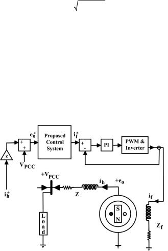
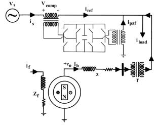
3. Connection of Electromechanical Filter
Figure 3, shows schematic of the proposed compensator system. In this research load current harmonics with higher order than 7, has been determined as PAF of UPQC compensator signal. But, load current harmonics with lower order than 7 and reactive power have been compensated by the proposed electromechanical filter.
Figure 3. Proposed compensator system
4. Electromechanical Parallel Active Filter
Figure 4, shows the simple structure of a synchronous generator. Based on equation (1), a DC field current of if produces a constant magnitude flux.
Ff N f i f , |
f |
N f i f |
, |
f |
N f Nsi f |
Mi f |
(1) |
R |
R |
As in [13] N f and Ns are effective turns of the field windings and the stator windings,
respectively; Ff is the magnetomotive force; R is the reluctance of the flux line direction and M is the mutual induction between rotor and stator windings. Speed of rotor is equal to the synchronous speed ( ns 120 f p ). Thus, the flux rotates with the angular speed of
82 An Update on Power Quality
s 2ns 60 . So, stator windings passing flux has been changed as equation (2). It is
assumed that in t 0 , direct axis of field and stator first phase windings conform each other.
s i f M cos(t) |
(2) |
The scope of this section is theoretically investigation of a synchronous machine as a rotating active filter. This theory will be investigated in the static state for a circular rotor type synchronous generator that its equivalent circuit has been shown in Figure 5.
Figure 4. Simple structure of synchronous generator
Figure 5. Equivalent circuit of synchronous generator
Equation (3) shows the relation between magnetic flux and voltage behind synchronous reactance of the generator.
e |
d s |
(t) |
|
|
d(i f |
M cos(t)) |
|
M |
d(i f |
cos(t)) |
(3) |
|
|
dt |
|
|
dt |
|
dt |
||||
|
|
|
|
|
|
|
|
|

Electromechanical Active Filter as a Novel Custom Power Device (CP) 83
Based on equation (3), if the field current be a DC current, the stator induction voltage will be a sinusoidal voltage by the amplitude of M i f . But, if the field current be harmonized as
equation (4) then, the flux and internal induction voltage will be as equations (5) and (6), respectively.
i f Idc I fn sin(n t fn )
n
f |
i f M cos(t) [Idc |
I fn sin(n t fn )]M cos(t) |
|||||||||||||
|
|
|
|
|
1 |
|
|
n |
|
|
|
|
|
||
MIdc cos(t) |
M I fn[sin((n 1) t fn ) sin((n 1) t fn )] |
||||||||||||||
|
|||||||||||||||
|
|
2 |
|
|
|
|
|
|
|
|
|
||||
|
e [MI sin(t) |
|
1 |
MI |
cos(t |
f 2 |
)] |
||||||||
|
|
||||||||||||||
|
o |
|
|
dc |
2 |
|
f 2 |
|
|||||||
|
|
|
1 |
|
|
|
|
|
1 |
|
|
|
|||
|
[ |
MI f (n 1)n cos(n t f (n 1) ) |
MI f (n 1)n cos(n t f (n 1) )] |
||||||||||||
|
|
|
|||||||||||||
|
n 2 |
2 |
|
|
|
|
|
|
2 |
|
|
|
|||
(4)
(5)
(6)
Equation (6) shows that each component of the generator output voltage has composed of two components of the field current. This problem has been shown in Figure 6.
Figure 6. Relation of the field current components by the stator voltage components
It seems that a synchronous generator can be assumed as the Current Controlled System (CCS). Thus it can be used for the current harmonic compensation of a nonlinear load ( Ihn ) as parallel active filter.
5. Algorithm and method
From Figure 5, relation between terminal voltage of the generator and Ihn can be derived as equation (7).
eo Vpcc ZnIhn Vn sin(n t n ) |
(7) |
n |
|
84 An Update on Power Quality
Where, n is the harmonic order; Zn R jnX is the harmonic impedance of the synchronous generator and connector transformer which are known, VPCC is the point of common coupling voltage and Ihn is the compensator current that has been extracted from the control circuit.
If similar frequency components of voltage signal eo in equation (6) and eo in equation (7) set equal, the magnitude and phase angle of the related field current components will be extracted as:
For n=1:
MIdc sin(t) 1 MI f 2 cos(t f 2 ) V1 sin(t 1) 2
[MI |
1 |
MI |
f 2 |
sin |
f |
2 |
]2 |
[ |
1 |
MI |
|
cos |
f 2 |
]2 |
V |
||||||
|
|
|
|||||||||||||||||||
dc |
2 |
|
|
|
|
|
|
|
2 |
|
f 2 |
|
1 |
||||||||
|
|
|
|
|
|
|
|
|
|
|
|
|
|
|
|
|
|
||||
|
|
|
|
|
|
1 |
MI |
|
cos |
f 2 |
|
|
|
|
|
|
|||||
|
|
|
|
|
|
|
|
|
|
|
|
|
|
||||||||
tan 1[ |
|
|
2 |
|
f 2 |
|
|
|
|
|
|
] 1 |
|
|
|
||||||
MI |
|
|
1 |
MI |
sin |
|
|
|
|
||||||||||||
|
|
|
|
|
f 2 |
|
|
|
|||||||||||||
|
|
|
|
|
|
|
|
||||||||||||||
|
|
|
|
|
dc |
2 |
|
|
|
f 2 |
|
|
|
|
|
|
|||||
|
|
|
|
|
|
|
|
|
|
|
|
|
|
|
|
|
|
|
|
|
|
For simplicity equations (9) and (10) can be rewritten as follows:
X MIdc 1 MI f 2 sin f 2 2
Y 1 MI f 2 cos f 2 2
X2 Y2 V12
X Y 1
(8)
(9)
(10)
(11)
(12)
(13)
(14)
From the above equations, magnitude and phase of the second component of filed current can result in:
X |
|
|
V1 |
|
(15) |
|
|
1 tan2 1 |
|||||
|
|
|
||||
tan f 2 |
|
X MIdc |
(16) |
|||
X tan1 |
||||||
|
|
|
|
|||
Electromechanical Active Filter as a Novel Custom Power Device (CP) 85
|
|
|
|
|
|
|
I f 2 |
2(X MIdc) |
|
|||||||||
|
|
|
|
|
|
|
|
M sin f 2 |
||||||||||
|
|
|
|
|
|
|
|
|
||||||||||
For n≥2: |
|
|
|
|
|
|
|
|
|
|
|
|
|
|
|
|
|
|
X |
1 |
|
MI f (n 1)n sin f (n 1) |
|
1 |
|
MI f (n 1)n sin f (n 1) |
|||||||||||
2 |
|
|
|
|||||||||||||||
|
|
|
|
|
|
|
|
|
2 |
|
|
|
|
|
|
|||
Y |
|
1 |
MI f (n 1)n cos f (n 1) |
|
1 |
MI f (n 1)n cosf (n 1) |
||||||||||||
|
2 |
|
||||||||||||||||
|
|
|
|
|
|
|
|
|
2 |
|
|
|
|
|
|
|||
|
|
|
|
|
|
|
X |
|
Vn |
|
||||||||
|
|
|
|
|
|
|
|
1 tan2 n |
||||||||||
|
|
|
|
|
|
|
|
|
||||||||||
tan f (n 1) |
|
|
X 0.5Mn I f (n 1) sin f (n 1) |
|
||||||||||||||
|
X tan n |
0.5Mn I f (n 1) cos f (n 1) |
||||||||||||||||
|
|
|
|
|
|
|
||||||||||||
|
|
|
|
I f (n 1) |
|
2(X 0.5Mn I f (n 1) sin f (n 1) ) |
||||||||||||
|
|
|
|
|
|
Mn sin f (n 1) |
|
|||||||||||
|
|
|
|
|
|
|
|
|
|
|
|
|
|
|
|
|
||
(17)
(18)
(19)
(20)
(21)
(22)
Where, M and are the mutual inductance and angular frequency, respectively. Obviously for the extraction of required components of filed current from the above equations, first suggestion for DC and first order component of the field current are need. Resulted field current can be injected via a PWM and current inverter to the field windings of the synchronous generator. Figure 7, shows the control circuit of the electromechanical
Figure 7. Block diagram of the proposed active filter control
86 An Update on Power Quality
active filter. Ih and I f are desired compensator current and calculated field current signal.
Detail of the proposed control circuit can be found in the equations (11) to (22). In the present research controlled voltage source of MATLAB has been used instead of required PWM and inverter. Constant and integrator coefficients in the PI controller have been chosen 1000 and 200, respectively. As mentioned earlier first order load active and reactive powers can be easily attended in the electromechanically compensated share of load current for decrease of SAF and PAF power range of UPQC. This problem can control power flow as well as power quality. In other word it can be possible to use a synchronous generator not only for first order voltage generation but, also for the harmonic compensation too.
6. Results
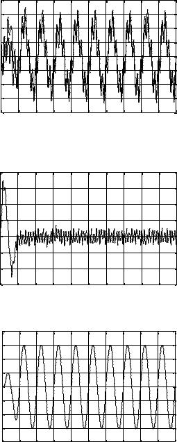
For the investigation of the validity of the mentioned control strategy for power quality compensation of a distribution system, simulation of the test circuit of Figure 8, has been done in MATLAB software. Source current and load voltage, have been measured and analyzed in the proposed control system for the determination of the compensator signals of SAF, PAF and filed current of the electromechanical active filter. Related equations of the controlled system and proposed model of the electromechanical active filter as a current controlled source have been compiled in MATLAB software via M-file. In mentioned control strategy, voltage harmonics have been compensated by SAF of the UPQC and current harmonics with higher order than 7, have been compensated by PAF of UPQC. But, the total of load reactive power, 25 percent of load active power and load current harmonics with lower order than 7 have been compensated by the proposed CCS. This power system consists of a harmonized and unbalanced three phase 380V (RMS, L-L), 50 Hz utility, a three phase balanced R-L load and a three phase rectifier as a nonlinear load. For the investigation of the
Figure 8. General test system circuit
Electromechanical Active Filter as a Novel Custom Power Device (CP) 87
voltage harmonic condition, utility voltages have harmonic and negative sequence components between 0.05 s and 0.2 s. Also, for the investigation of the proposed control strategy in unbalance condition, magnitude of the first phase voltage is increased to the 1.25 pu between 0.05 s and 0.1 s and decreased to the 0.75 pu between 0.15 s to 0.2 s. Table 1, shows the utility voltage harmonic and sequence parameters data and Table 2, shows the load power and voltage parameters. A number of selected simulation results will be showed further.
|
|
Voltage Order |
Sequence |
Magnitude (pu) |
Phase Angle (deg) |
|
|||
|
|
|
|
|
|
|
|
|
|
|
|
5 |
|
1 |
|
0.12 |
-45 |
|
|
|
|
3 |
|
2 |
|
0.1 |
0 |
|
|
Table 1. |
Utility voltage harmonic and sequence parameters data |
|
|
||||||
|
|
|
|
|
|
||||
|
Load |
Nominal Power (kVA) |
|
Nominal Voltage (RMS, L-L) |
|
||||
|
Linear |
10 |
|
|
|
380V |
|
||
|
Non linear |
5 |
|
|
|
380V |
|
||
Table 2. |
Load power and voltage parameters data |
|
|
|
|
||||
Figure 9, shows the source side voltage of phase 1. Figure 10, shows the compensator voltage of phase 1. Figure 11, shows load side voltage of phase 1. Figure 12, shows the load side current of phase 1. Figure 13, shows the CCS current of phase 1 that has been supplied by the proposed active filter. Figure 14, shows the PAF of UPQC current of phase 1. Figure 15, shows the source side current of phase 1. Figure 16, shows the field current of the proposed harmonic filter. Figure 17 and 18 show source voltage and load voltage frequency spectrum, respectively. Figure 19 and 20 show load current and source current frequency spectrum, respectively. Figure 21 and 22 show CCS and PAF frequency spectrum, respectively. Table 3 shows THDs of source and load voltages and currents. Load voltage and source current harmonics have been compensated satisfactory.
|
400 |
|
|
|
|
|
|
|
|
|
|
|
300 |
|
|
|
|
|
|
|
|
|
|
|
200 |
|
|
|
|
|
|
|
|
|
|
(V) |
100 |
|
|
|
|
|
|
|
|
|
|
|
|
|
|
|
|
|
|
|
|
|
|
Voltage |
0 |
|
|
|
|
|
|
|
|
|
|
-100 |
|
|
|
|
|
|
|
|
|
|
|
|
|
|
|
|
|
|
|
|
|
|
|
|
-200 |
|
|
|
|
|
|
|
|
|
|
|
-300 |
|
|
|
|
|
|
|
|
|
|
|
-4000 |
0.02 |
0.04 |
0.06 |
0.08 |
0.1 |
0.12 |
0.14 |
0.16 |
0.18 |
0.2 |
Time (Sec)
Figure 9. Source side voltage of phase 1 (swell has been occurred between 0.05 and 0.1 sec and sag has been occurred between 0.15 and 0.2 sec. Also, harmonics of positive and negative sequences have been concluded between 0.05 to 0.2 sec)
88 An Update on Power Quality
|
150 |
|
|
|
|
|
|
|
|
|
|
|
100 |
|
|
|
|
|
|
|
|
|
|
(V) |
50 |
|
|
|
|
|
|
|
|
|
|
|
|
|
|
|
|
|
|
|
|
|
|
Voltage |
0 |
|
|
|
|
|
|
|
|
|
|
|
|
|
|
|
|
|
|
|
|
|
|
|
-50 |
|
|
|
|
|
|
|
|
|
|
|
-100 |
|
|
|
|
|
|
|
|
|
|
|
-1500 |
0.02 |
0.04 |
0.06 |
0.08 |
0.1 |
0.12 |
0.14 |
0.16 |
0.18 |
0.2 |
Time (Sec)
Figure 10. Compensator voltage of phase 1 (compensator voltage has been determined for the sag, swell, negative sequence and harmonics improvement)
|
400 |
|
|
|
|
|
|
|
|
|
|
|
300 |
|
|
|
|
|
|
|
|
|
|
|
200 |
|
|
|
|
|
|
|
|
|
|
(V) |
100 |
|
|
|
|
|
|
|
|
|
|
|
|
|
|
|
|
|
|
|
|
|
|
Voltage |
0 |
|
|
|
|
|
|
|
|
|
|
-100 |
|
|
|
|
|
|
|
|
|
|
|
|
|
|
|
|
|
|
|
|
|
|
|
|
-200 |
|
|
|
|
|
|
|
|
|
|
|
-300 |
|
|
|
|
|
|
|
|
|
|
|
-4000 |
0.02 |
0.04 |
0.06 |
0.08 |
0.1 |
0.12 |
0.14 |
0.16 |
0.18 |
0.2 |
Time (Sec)
Figure 11. Load side voltage of phase 1 (sag, swell, harmonics, positive and negative sequences have been canceled)
|
40 |
|
|
|
|
|
|
|
|
|
|
|
30 |
|
|
|
|
|
|
|
|
|
|
|
20 |
|
|
|
|
|
|
|
|
|
|
(A) |
10 |
|
|
|
|
|
|
|
|
|
|
|
|
|
|
|
|
|
|
|
|
|
|
Current |
0 |
|
|
|
|
|
|
|
|
|
|
-10 |
|
|
|
|
|
|
|
|
|
|
|
|
|
|
|
|
|
|
|
|
|
|
|
|
-20 |
|
|
|
|
|
|
|
|
|
|
|
-30 |
|
|
|
|
|
|
|
|
|
|
|
-400 |
0.02 |
0.04 |
0.06 |
0.08 |
0.1 |
0.12 |
0.14 |
0.16 |
0.18 |
0.2 |
Time (Sec)
Figure 12. Load side current of phase 1 (it is harmonized. It should be noticed that this current has been calculated after the voltage compensation and thus voltage unbalance has not been transmitted to the current)
Electromechanical Active Filter as a Novel Custom Power Device (CP) 89
|
20 |
|
|
|
|
|
|
|
|
|
|
|
15 |
|
|
|
|
|
|
|
|
|
|
|
10 |
|
|
|
|
|
|
|
|
|
|
(A) |
5 |
|
|
|
|
|
|
|
|
|
|
|
|
|
|
|
|
|
|
|
|
|
|
Current |
0 |
|
|
|
|
|
|
|
|
|
|
-5 |
|
|
|
|
|
|
|
|
|
|
|
|
|
|
|
|
|
|
|
|
|
|
|
|
-10 |
|
|
|
|
|
|
|
|
|
|
|
-15 |
|
|
|
|
|
|
|
|
|
|
|
-200 |
0.02 |
0.04 |
0.06 |
0.08 |
0.1 |
0.12 |
0.14 |
0.16 |
0.18 |
0.2 |
Time (Sec)
Figure 13. Proposed CCS current of phase 1 (this current has been injected to the grid by the electromechanical active filter. The solid line shows output current of filter and dotted line shows desired current of filter)
|
40 |
|
|
|
|
|
|
|
|
|
|
|
30 |
|
|
|
|
|
|
|
|
|
|
|
20 |
|
|
|
|
|
|
|
|
|
|
(A) |
10 |
|
|
|
|
|
|
|
|
|
|
Current |
0 |
|
|
|
|
|
|
|
|
|
|
|
|
|
|
|
|
|
|
|
|
|
|
|
-10 |
|
|
|
|
|
|
|
|
|
|
|
-20 |
|
|
|
|
|
|
|
|
|
|
|
-300 |
0.02 |
0.04 |
0.06 |
0.08 |
0.1 |
0.12 |
0.14 |
0.16 |
0.18 |
0.2 |
Time (Sec)
Figure 14. PAF of UPQC current of phase 1 (this current has been injected to the grid by the parallel active filter of UPQC)
|
40 |
|
|
|
|
|
|
|
|
|
|
|
30 |
|
|
|
|
|
|
|
|
|
|
|
20 |
|
|
|
|
|
|
|
|
|
|
(A) |
10 |
|
|
|
|
|
|
|
|
|
|
|
|
|
|
|
|
|
|
|
|
|
|
Current |
0 |
|
|
|
|
|
|
|
|
|
|
-10 |
|
|
|
|
|
|
|
|
|
|
|
|
|
|
|
|
|
|
|
|
|
|
|
|
-20 |
|
|
|
|
|
|
|
|
|
|
|
-30 |
|
|
|
|
|
|
|
|
|
|
|
-400 |
0.02 |
0.04 |
0.06 |
0.08 |
0.1 |
0.12 |
0.14 |
0.16 |
0.18 |
0.2 |
Time (Sec)
Figure 15. Source side current of phase 1 (harmonics and reactive components of load current have been canceled)
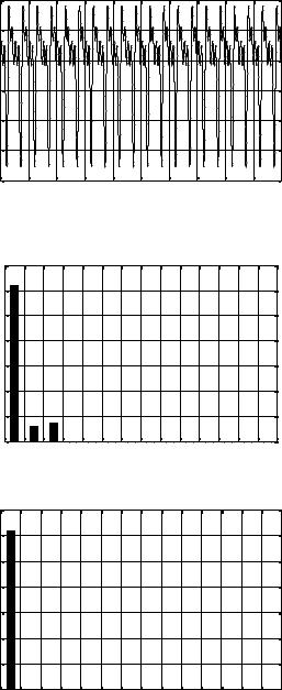
90 An Update on Power Quality
|
1400 |
|
|
|
|
|
|
|
|
|
|
|
1200 |
|
|
|
|
|
|
|
|
|
|
(A) |
1000 |
|
|
|
|
|
|
|
|
|
|
|
|
|
|
|
|
|
|
|
|
|
|
Current |
800 |
|
|
|
|
|
|
|
|
|
|
|
|
|
|
|
|
|
|
|
|
|
|
|
600 |
|
|
|
|
|
|
|
|
|
|
|
400 |
|
|
|
|
|
|
|
|
|
|
|
2000 |
0.02 |
0.04 |
0.06 |
0.08 |
0.1 |
0.12 |
0.14 |
0.16 |
0.18 |
0.2 |
Time (Sec)
Figure 16. Field current of proposed harmonic filter (field current is controlled for the load active, reactive and harmonic current compensation)
Amplitude (V)
350 
300
250
200
150
100
50
00 |
100 |
200 |
300 |
400 |
500 |
600 |
700 |
800 |
900 |
1,0001,100 1,200 1,3001,400 |
Frequency (Hz)
Figure 17. Source side voltage frequency spectrum
Amplitude (V)
350 
300
250
200
150
100
50
00 |
100 |
200 |
300 |
400 |
500 |
600 |
700 |
800 |
900 |
1000 1100 1200 1300 1400 |
Frequency (Hz)
Figure 18. Load side voltage frequency spectrum
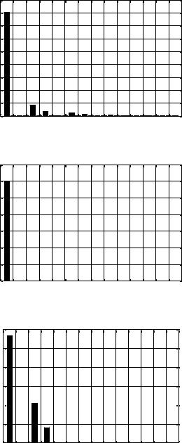
Electromechanical Active Filter as a Novel Custom Power Device (CP) 91
|
45 |
|
|
|
|
|
|
|
|
|
|
|
40 |
|
|
|
|
|
|
|
|
|
|
|
35 |
|
|
|
|
|
|
|
|
|
|
(A) |
30 |
|
|
|
|
|
|
|
|
|
|
|
|
|
|
|
|
|
|
|
|
|
|
Amplitude |
25 |
|
|
|
|
|
|
|
|
|
|
20 |
|
|
|
|
|
|
|
|
|
|
|
15 |
|
|
|
|
|
|
|
|
|
|
|
|
|
|
|
|
|
|
|
|
|
|
|
|
10 |
|
|
|
|
|
|
|
|
|
|
|
5 |
|
|
|
|
|
|
|
|
|
|
|
00 |
100 |
200 |
300 |
400 |
500 |
600 |
700 |
800 |
900 |
1000 1100 1200 1300 1400 |
Frequency (Hz)
Figure 19. Load side current frequency spectrum
35
Amplitude (A)
30
25
20
15
10
5
00 |
100 |
200 |
300 |
400 |
500 |
600 |
700 |
800 |
900 |
1000 1100 1200 1300 1400 |
Frequency (Hz)
Figure 20. Source side current frequency spectrum
12 
Amplitude (A)
10
8
6
4 


2
00 |
100 |
200 |
300 |
400 |
500 |
600 |
700 |
800 |
900 |
1000 1100 1200 1300 1400 |
Frequency (Hz)
Figure 21. Proposed current controlled system frequency spectrum
92 An Update on Power Quality
|
1.4 |
|
|
|
|
|
|
|
|
|
|
|
1.2 |
|
|
|
|
|
|
|
|
|
|
|
1 |
|
|
|
|
|
|
|
|
|
|
(A) |
0.8 |
|
|
|
|
|
|
|
|
|
|
Amplitude |
|
|
|
|
|
|
|
|
|
|
|
0.6 |
|
|
|
|
|
|
|
|
|
|
|
|
|
|
|
|
|
|
|
|
|
|
|
|
0.4 |
|
|
|
|
|
|
|
|
|
|
|
0.2 |
|
|
|
|
|
|
|
|
|
|
|
00 |
100 |
200 |
300 |
400 |
500 |
600 |
700 |
800 |
900 |
1000 1100 1200 1300 1400 |
Frequency (Hz)
Figure 22. Parallel active filter frequency spectrum
VS THD |
IL THD |
VL THD |
IS THD |
|
|
|
|
0.1561 |
0.1179 |
.001 |
.0012 |
|
|
|
|
Table 3. Total Harmonic Distortion (THD)
7. Conclusions
It is known that use of small synchronous generators in distributed generated networks can reduce transmitted active and reactive powers from the main source and consequently line losses. In this research power quality compensation was done by composition of UPQC and synchronous generators as electromechanical active filter. In other word, by proper determination and control of synchronous generator field current it could be used as controlled current source for power quality compensation. This was for reduction of UPQC power rating in the distributed generated networks. Also, an algorithm was investigated for the determination of the reference field current. Proposed CCS modeling was implemented based on the mentioned related algorithm in MATLAB software. Control strategy had three instantaneously stages. Voltage harmonics were compensated by SAF of the UPQC. Current harmonics with higher order than 7 were compensated by PAF of the UPQC. Lower order current harmonics, load reactive power and a part of load active power were compensated by the proposed controlled current source. Total harmonic distortion of load voltage before compensation was 0.15 which was reduced to almost zero after compensation. Also, total harmonic distortion of the source current before compensation was 0.12 which was reduced to almost zero after compensation.
Electromechanical Active Filter as a Novel Custom Power Device (CP) 93
Author details
Ahad Mokhtarpour, Heidarali Shayanfar and Mitra Sarhangzadeh
Department of Electrical Engineering, Tabriz Branch, Islamic Azad University, Tabriz, Iran
8. References
[1]Fujita H., Akagi H. The Unified Power Quality Conditioner: The Integration of Series and Shunt Active Filters. IEEE Transaction on Power Electronics 1998; 13(2) 315-322.
[2]Shayanfar H. A., Mokhtarpour A. Management, Control and Automation of Power Quality Improvement. In: Eberhard A. (ed.) Power Quality. Austria: InTech; 2010. p127152.
[3]Hannan M. A., Mohamed A. PSCAD/EMTDC Simulation of Unified Series-Shunt Compensator for Power Quality Improvement. IEEE Transaction on Power Delivery 2005; 20(2) 1650-1656.
[4]Han Y., Khan M.M., Yao G., Zhou L.D., Chen C. A novel harmonic-free power factor corrector based on T-type APF with adaptive linear neural network (ADALINE) control. Simulation Modeling Practice and Theory 2008; 16 (9) 1215– 1238.
[5]Khadkikar V., Chandra A. A Novel Structure for Three Phase Four Wire Distribution System Utilizing Unified Power Quality Conditioner (UPQC). IEEE Transactions on Industry Applications 2009; 45(5) 1897-1902.
[6]Kwan K. H., Chu Y.C., So P.L. Model-Based H∞ Control of a Unified Power Quality Conditioner. IEEE Transactions on Industrial Electronics 2009; 56 (7) 2493-2504.
[7]Khadkikar V., Chandra A. A New Control Philosophy for a Unified Power Quality Conditioner (UPQC) to Coordinate Load-Reactive Power Demand between Shunt and Series Inverters. IEEE Transactions on Power Delivery 2008; 23 (4) 2522-2534.
[8]Lee W.C., Lee D.M., Lee T.K. New Control Scheme for a Unified Power Quality Compensator-Q with Minimum Active Power Injection. IEEE Transactions on Power Delivery 2010; 25(2) 1068-1076.
[9]Han B., Bae B., Kim H., Baek S. Combined Operation of Unified Power-Quality Conditioner with Distributed Generation. IEEE Transaction on Power Delivery 2006; 21(1) 330-338.
[10]Mohammadi H.R., Varjani A.Y., Mokhtari H. Multiconverter Unified Power-Quality Conditioning System: MC-UPQC. IEEE Transactions on Power Delivery 2009; 24(3) 1679-1686.
[11]Jindal A.K., Ghosh A., Joshi A. Interline Unified Power Quality Conditioner. IEEE Transactions on Power Delivery 2007; 22(1) 364-372.
94An Update on Power Quality
[12]Mokhtarpour A., Shayanfar H.A., Tabatabaei N.M. Power Quality Compensation in two Independent Distribution Feeders. International Journal for Knowledge, Science and Technology 2009; 1 (1) 98-105.
[13]Machowski J., Bialek J., Bumby J.R. Power System Dynamics and Stability, United Kingdom: John Wiley and Sons; 1997.

Chapter 6
Reference Generation
of Custom Power Devices (CPs)
Ahad Mokhtarpour, Heidarali Shayanfar
and Seiied Mohammad Taghi Bathaee
Additional information is available at the end of the chapter
http://dx.doi.org/10.5772/54680
1. Introduction
One of the serious problems in electrical power systems is the increase of electronic devices which are used by the industry. These devices, which need high-quality energy to work properly, at the same time, are the most responsible ones for decreasing of power quality by themselves.
Custom power devices (CP) used in distribution systems can control power quality. One of the most efficient CPs is Unified Power Quality Conditioner (UPQC). It consists of a Parallel-Active Filter (PAF) and a Series-Active Filter (SAF) together with a common dc link [1-3]. This combination allows a simultaneous compensation for source side currents and delivered voltage to the load. In this way, operation of the UPQC isolates the utility from current quality problems of the load and at the same time isolates the load from the voltage quality problems of utility.
Reference generation of UPQC is an important problem. One of the scopes of this research is extending of Fourier transform for increasing of its responsibility speed twelve times as the main control part of reference generation of the UPQC. Proposed approach named Very Fast Fourier Transform (VFFT) can be used in balanced three phase systems for extraction of reference voltage and current signals. Proposed approach has fast responsibility as well as good steady state response. As it is known, Fourier transform response needs at least one cycle data for the settling down which results in slow responsibility and week capability in dynamic condition. In the proposed approach there are two different data window lengths. In the sag or swell condition, control system switches to T/12 data window length but, in the steady state condition it is switched to T/2 data window length. It causes fast responsibility as well as good steady state response. This approach will be used for the UPQC control circuit for extraction of the reference signals.

96 An Update on Power Quality
Second scope of this research is to use Multy Output ADAptive LINEar (MOADALINE) approach for the reference generation of UPQC. Simplicity and flexibility in extraction of different reference signals can be advantage of the proposed algorithm. Third scope of this research is reference generation of UPQC with the scope of power flow control as well as power quality compensation. In this stage, SAF is controlled by dqo approach for voltage sag, swell, unbalance, interruption, harmonic compensation and power flow control. Also, PAF is controlled by composition of dqo and Fourier theories for current harmonic and reactive power compensation.
Also for the validity of the proposed approaches, power quality compensation has been done in a test circuit via simulation. Voltage sag, swell and harmonics will be compensated by SAF of UPQC. Also, current harmonics and reactive power will be compensated by PAF of UPQC. Section 2 generally introduces UPQC and its equivalent circuit. Section 3 explains the proposed VFFT and related equations. Section 4 introduces UPQC reference generation system based on the proposed VFFT approach. Section 5 explains proposed MOADALINE algorithm for reference generation. Section 6 explains reference generation based on power flow control. Section 7 simulates the research. Finally, section 8 concludes the results.
2. Unified Power Quality Conditioner (UPQC)
UPQC is composed of two inverters that are connected back to back [3-10]. One of them is connected to the grid via a parallel transformer and can compensate the current problems (PAF). Another one is connected to the grid via a series transformer and can compensate the voltage problems (SAF). These inverters are controlled for the compensation of the power quality problems instantaneously. Figure 1 shows the general schematic of a UPQC.
Figure 1. General schematic of a UPQC
A simple circuit model of the UPQC is shown in Figure 2. Series active filter has been modeled as the voltage source and parallel active filter has been modeled as the current source.
Figure 2. Circuit model of UPQC
Reference Generation of Custom Power Devices (CPs) 97
3. VFFT problem statement
Fourier transform has the capability of different order components extraction of distorted periodic voltage and current. It is possible to use voltage and current first order components for determining the compensator signals. Based on the related equations of Fourier transform, there is a need for at least one cycle data for settling down the response. This problem can cause week responsibility in dynamic condition. Proposed extended Fourier transform will be responsible for improving this problem. First order Fourier coefficients of a sinusoidal signal can be written as equations (1) and (2).
|
2 |
|
2 |
|
|
4 |
|
|
|||
a1 |
|
|
|
0 |
v( t)cos( t)d t |
|
|
|
0 |
v( t)cos( t)d t |
(1) |
2 |
|
2 |
|||||||||
|
2 |
|
2 |
|
|
4 |
|
|
|||
b1 |
|
|
0 |
v( t)sin( t)d t |
|
|
0 |
v( t)sin( t)d t |
(2) |
||
|
2 |
2 |
|||||||||
Based on equations (1) and (2) it is possible to reduce settling time of the Fourier transform responsibility to T/2; where, T is the main period of the signal. In this condition the responsibility speed will be increased twice but, it is not reasonable speed in dynamic condition yet. Equation (5) can be resulted from equations (3) and (4), for a sinusoidal signal with phase angle Φ. Equation (6) can be resulted similarly.
|
|
|
|
|
|
|
|
|
|
|
|
|
4 |
|
|
|
|
|
|
|
|
|
|
|
|
|
|
|
||
|
|
|
|
|
|
|
|
|
|
|
|
|
|
0 sin( t )cos( t)d t sin |
||||||||||||||||
|
|
|
|
|
|
|
|
|
|
|
|
|
2 |
|||||||||||||||||
|
8 |
|
|
|
|
|
|
|
|
|
|
8 |
|
|
|
|
3 |
|||||||||||||
|
|
06 sin( t )cos( t)d t |
|
|
|
|
26 |
|
sin( t )cos( t)d t |
|||||||||||||||||||||
|
|
2 |
|
|
2 |
|
||||||||||||||||||||||||
|
|
|
|
|
|
|
|
|
|
5 |
|
|
|
|
|
|
|
|
|
|
|
|
|
6 |
|
|
||||
|
8 |
|
|
|
|
|
|
|
|
|
|
|
|
|
|
|
|
|
|
|||||||||||
|
|
46 |
|
sin( t )cos( t)d t sin |
||||||||||||||||||||||||||
|
|
2 |
|
|
||||||||||||||||||||||||||
|
|
|
|
|
|
|
6 |
|
|
|
|
|
|
|
|
|
|
|
|
|
|
|
|
|
|
|
|
|||
4 |
|
|
|
|
|
|
|
|
|
|
|
|
|
|
|
8 |
|
|
|
|
|
|
|
|
||||||
|
|
|
|
|
|
|
|
|
|
|
|
|
|
|
|
|
|
|
|
|
|
|
|
|
|
|||||
|
|
0 |
sin( t )cos( t)d t |
|
|
|
|
06 sin( t )cos( t)d t |
||||||||||||||||||||||
2 |
2 |
|||||||||||||||||||||||||||||
8 |
|
|
|
|
3 |
8 |
|
|
|
5 |
|
|
|
|||||||||||||||||
|
|
|
|
|
|
|
|
|
|
|
|
|
|
|
|
|
|
|
|
|
|
|||||||||
|
|
26 |
|
sin( t )cos( t)d t |
|
|
|
46 |
sin( t )cos( t)d t sin |
|||||||||||||||||||||
2 |
2 |
|||||||||||||||||||||||||||||
|
6 |
|
|
|
|
|
|
|
|
|
|
|
|
|
|
|
6 |
|
|
|
|
|||||||||
4 |
|
|
|
|
|
|
|
|
|
|
|
|
|
|
|
8 |
|
|
|
|
|
|
|
|
||||||
|
|
|
|
|
|
|
|
|
|
|
|
|
|
|
|
|
|
|
|
|
|
|
|
|
|
|||||
|
0 |
sin( t )sin( t)d t |
|
|
|
|
06 sin( t )sin( t)d t |
|||||||||||||||||||||||
2 |
|
2 |
||||||||||||||||||||||||||||
8 |
|
|
|
3 |
8 |
|
|
|
|
5 |
|
|
|
|||||||||||||||||
|
|
|
|
|
|
|
|
|
|
|
|
|
|
|
|
|
|
|
|
|
|
|||||||||
|
26 |
|
|
sin( t )sin( t)d t |
|
46 |
|
sin( t )sin( t)d t cos |
||||||||||||||||||||||
2 |
|
|
2 |
|||||||||||||||||||||||||||
|
6 |
|
|
|
|
|
|
|
|
|
|
|
|
|
|
|
6 |
|
|
|
|
|||||||||
Equations (7) and (8) can be rewritten from equations (5) and (6) respectively.
(3)
(4)
(5)
(6)

98 An Update on Power Quality
|
|
|
|
8 |
|
|
|
|
|
8 |
|
|
|
|
|
|
|
|
|
|
|
|||||||
a1 |
|
06 sin(t )cos(t)d t |
|
06 (sin(t 2 |
3))(cos(t 2 |
3))d t |
||||||||||||||||||||||
2 |
2 |
|
||||||||||||||||||||||||||
8 |
|
|
|
|
|
|
|
|
|
|
|
|
|
|
8 |
|
|
|
|
|
|
|
|
|
|
|||
|
06 sin(t 2 |
3)cos(t 2 |
3)d t |
|
|
06 sin(t )cos(t)d t |
|
|
|
(7) |
||||||||||||||||||
2 |
|
|
2 |
|
|
|
||||||||||||||||||||||
8 |
|
|
|
|
|
|
|
|
|
|
|
|
|
|
|
|
8 |
|
|
|
|
|
|
|
|
|
|
|
|
6 sin(t 2 |
|
)cos(t 2 |
|
)d t |
|
|
6 sin(t 2 |
|
)cos(t |
2 |
|
)d t |
|||||||||||||||
2 |
3 |
3 |
2 |
|
3 |
3 |
||||||||||||||||||||||
0 |
|
|
|
|
|
|
|
|
|
|
0 |
|
|
|
|
|
||||||||||||
|
|
|
|
|
8 |
|
|
|
|
8 |
|
|
|
|
|
|
|
|
|
|
|
|||||||
b1 |
|
06 sin(t )sin(t)d t |
|
06 (sin(t 2 |
3))(sin(t 2 |
|
3))d t |
|||||||||||||||||||||
2 |
|
2 |
|
|
||||||||||||||||||||||||
|
8 |
|
|
|
|
|
|
|
|
|
|
|
|
|
8 |
|
|
|
|
|
|
|
|
|
|
|||
|
|
06 sin(t 2 |
3)sin(t 2 |
3)d t |
|
|
06 sin(t )sin(t)d t |
|
|
|
(8) |
|||||||||||||||||
|
2 |
|
|
2 |
|
|
|
|
||||||||||||||||||||
8 |
|
|
|
|
|
|
|
|
|
|
|
|
|
|
|
8 |
|
|
|
|
|
|
|
|
|
|||
|
6 sin(t 2 |
|
)sin(t 2 |
|
)d t |
|
6 sin(t 2 |
|
)sin(t 2 |
|
)d t |
|||||||||||||||||
|
2 |
|
3 |
3 |
|
|
3 |
3 |
||||||||||||||||||||
|
0 |
|
|
|
|
|
|
|
|
|
|
2 |
0 |
|
|
|
|
|
||||||||||
This solution has advantage of reducing the data window length to T/12. In this condition, settling time of the Fourier transform responsibility will be decreased to T/12. In other words, the responsibility speed will be increased twelve times. It should be noticed that this approach can be used only in balanced three phase systems. In this condition reach to the same accuracy in response is possible as compared to that of one cycle but very faster than one cycle. When data window length is chosen T sec, all of even components of distorted voltage and current in the related integral of Fourier transform can be filtered completely. But this is not possible in T/12 data window length condition. So, the problem of this approach is the unfiltered steady state oscillations in the response. This is because of small data window length. Thus, to complete the proposed approach for accessing the fast response, as well as good steady state response, proper composition of T/12 and T/2 data window lengths have been used. Completed proposed approach uses T/12 data window length in signal magnitude change instances, for accessing the fast response, and T/2 data window length in other times, for accessing the good response without oscillation [10].
4. UPQC reference generation based on the VFFT
Based on the previous indications, the detection of sag, swell, and load change conditions are essential problem for proper control of the UPQC. In this research, for the detection of sag or swell condition in the source voltage and changes in the load current, derivative of the first order component magnitude of the voltage and current signals has been compared with a constant value. This is based on the facts that in these conditions, the derivative of the signal magnitude can change rapidly with an almost increasing slope amount. Figure 3, shows the block diagram of the proposed VFFT based control approach [10].
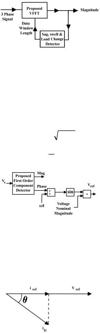
Reference Generation of Custom Power Devices (CPs) 99
Figure 3. Proposed VFFT based control system
4.1. Series active filter reference generation
Proposed approach can be used for the extraction of direct and indirect first order components of the source voltage. In this control approach, series active filter can compensate harmonics as well as voltage sag and swells. In this approach the reference voltage magnitude can be setup to the nominal value as equation (9). Figure 4, shows the block diagram of the SAF control circuit.
v |
(t) a |
cos(t) b |
sin(t) |
a2 |
b2 |
sin(t arctan |
a1 |
) |
|
|
|
||||||||
1 |
1 |
1 |
|
1 |
1 |
|
b1 |
(9) |
|
|
|
|
|
|
|
|
|||
a
vref (t) vnom sin(t arctan b1 ) vnom sin(t vl1)
1
Figure 4. SAF control system block diagram
4.2. Parallel active filter reference generation
In this research parallel active filter have the duty of the reactive power compensation, as well as, current harmonics. For this purpose as equation (10), active first order component of load current which is tangent component of the load current to the load voltage can be used as the reference current. This problem has been shown in Figure 5.
Figure 5. Reference current determination
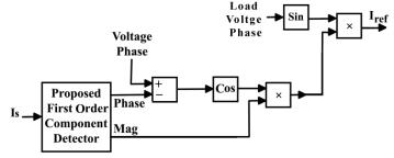
100 An Update on Power Quality
Iref (t) Il1 cos( vl1 il1)sin( t vl1) |
(10) |
Where, Il1 and Φil1 are the first order component magnitude and phase angle of the load current, respectively and Φvl1 is the first order component phase angle of the load voltage. Figure 6, shows the block diagram of the PAF control circuit.
Figure 6. Block diagram of the PAF control circuit
5. Reference generation based on MOADALINE approach
Based on MOADLINE approach each n 1 signal of y can be written as a weighted linear combination of its components. If S(t) be n m component matrix of y at time t and W(t) be m 1 vector of weighted coefficient then, the signal of y can be written as equation (11). MOADALINE can be used for determining weight vector of W which generates a special signal of y from its components [11]. Weighted factors can be updated in each stage of an adaptation approach for extraction of a desired signal. Equation (11) shows adaptation rule that is based on Least Mean Square (LMS) algorithm.
y SW
W(t dt) W(t) kST (t)[S(t)ST (t)] 1e(t) (11)
Where, e(t) is the error between desired and actual signal of y, and K is the convergence factor. It is possible to extract the reference voltage and current from uncompensated source voltage and load current. Fourier coefficients can be determined as vector of y. Reference signal can be determined as W. Matrix of S is constant. After determination of uncompensated signal Fourier coefficients, they can be compared with the desired values. Error signal can be used in adaptation rule for updating the vector of W. Therefore reference voltage and current can be determined. Figure 7, shows block diagram of the proposed MOADALINE approach [11].
a |
|
|
n |
(12) |
|
y bn |
||
a |
|
|
|
0 |
|
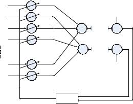
Reference Generation of Custom Power Devices (CPs) 101
|
|
|
|
|
|
|
|
cos(n t ) ... |
cos(n t |
|
|
|||||
|
2 |
|
cos(n t |
|
) |
m 1 |
) |
|||||||||
|
|
|
|
|
0 |
|
|
|
1 |
|
|
|
|
|||
S(t) |
|
|
sin(n t0 ) |
sin(n t1) ... |
sin(n tm 1) |
|||||||||||
m 1 |
||||||||||||||||
|
|
1 |
|
|
|
|
1 |
... |
|
1 |
|
|
|
|||
|
|
|
|
|
|
|
|
|
|
|||||||
|
|
|
|
2 |
|
|
|
2 |
|
2 |
|
|
|
|||
|
w(t0 ) |
|
|
|
w(t ) |
|
|
W |
|
1 |
|
... |
|
||
|
|
|
|
w(t |
m 1 |
) |
|
|
|
|
|
anbna0
|
|
|
|
|
|
2 |
|
cos(n t0 ) |
|||
|
|
|
|
||
|
|
sin(n t0 ) |
|||
m 1 |
|||||
|
1 |
|
|||
|
|
|
|
||
|
|
2 |
|
||
|
|
|
|
||
...
...
...
|
|
|
|
w(t0 ) |
|
|
|
|
|||
cos(n tm 1) |
|
w(t ) |
|||
sin(n tm 1) |
|
|
1 |
||
... |
|||||
1 |
|
|
|
|
|
|
|
|
|
w(t |
|
2 |
|
|
|
m 1 |
|
)
cos(wt0) |
W0 |
|
|
sin(wt0) |
|
|
a1 |
W0 |
|
|
|
|
|
|
|
cos(wt1) |
+ |
2/(m-1) |
- |
|
W1 |
|
|
sin(wt1) |
W1 |
|
|
|
|
|
|
|
+ |
2/(m-1) |
- |
coswt(m-1) |
|
|
b1 |
|
W(m-1) |
|
|
sinwt(m-1) |
|
|
|
|
W(m-1) |
|
|
|
Weighted |
|
|
|
Factors |
|
|
|
Calculation |
|
|
Figure 7. Block diagram of the proposed MOADALINE approach
(13)
(14)
(15)
6. Reference generation based on power flow control
Park transform which is used for the conversion of abc to dqo frame, is useful in the steady state and dynamic analysis of electrical systems [3]. Conversion matrix and related equations have been shown in Equations (16) and (17).
vdvqvo
|
|
2sin(t) |
2sin(t |
2 |
|
|
2sin(t |
2 |
|
|
|
|
|
|
|
|
|
|
|
|
) |
|
) |
|
|
|
|
|
|
|
|||||
|
3 |
3 |
v |
|
|
|
v |
|
|
||||||||
|
|
|
|
|
|
|
|
|
|
|
|
||||||
1 |
|
|
2 |
|
|
|
2 |
|
|
|
a |
|
|
|
a |
|
|
|
|
|
|
|
|
|
|
|
|||||||||
|
2cos( t) |
2cos( t |
|
|
) |
2cos( t |
|
|
) |
vb |
T vb |
(16) |
|||||
|
|
|
|
|
|||||||||||||
3 |
|
1 |
1 |
3 |
|
|
1 |
3 |
v |
|
|
|
v |
|
|
||
|
|
|
|
|
|
|
|
|
c |
|
|
|
c |
|
|||
|
|
|
|
|
|
|
|
|
|
|
|
|
|
|
|
|
|
|
|
|
|
|
|
|
|
|
|
|
|
|
|
|
|
|
|
102 An Update on Power Quality
va
vb T 1vc
vd
vq (17)vo
Instantaneous active and reactive powers in dqo axis can be written as Equations (18) and (19).
P |
3 |
(v i |
|
v i |
2v |
i |
|
) |
(18) |
|||||
|
|
|
||||||||||||
2 |
|
d |
d |
|
q q |
|
|
0 |
|
0 |
|
|
||
Q |
3 |
(v i |
|
v i |
|
) |
|
|
|
(19) |
||||
|
|
|
|
|
|
|||||||||
|
|
2 |
|
q |
d |
|
d |
q |
|
|
|
|
|
|
Equations (20) and (21) show direct and quadratic axis voltages based on P and Q that have been determined from equations (18) and (19). It should be noticed that the active and reactive powers in equations (20) and (21) are transmitted powers after series active filter toward the load. These equations show that in constant impedance loads there is a relation between voltage and transmitted power. In other words, a particular load voltage is needed for a particular load power and vice versa. In equations (20) and (21) it have been assumed that the voltages are balanced and v0 0 .
vd |
2 |
|
( |
|
Pid Qiq |
) |
(20) |
|||
3 |
|
|
id |
2 iq2 |
||||||
|
|
|
|
|
|
|
||||
vq |
|
2 |
( |
Piq Qid |
) |
(21) |
||||
|
|
|
||||||||
|
|
3 |
|
|
|
id |
2 iq2 |
|
|
|
Therefore, setup transmission active and reactive powers in equations (20) and (21) in considered amounts will result the related load voltage magnitude and phase angle. In reactive power compensated condition, Q=0 and the amount of active power will be extracted from the above equations as equation (22).
P |
3 |
(v |
2 v |
2 )(i |
2 i2 ) |
(22) |
|
||||||
2 |
d |
q |
d |
q |
|
|
|
|
|
|
|
||
Generally, in this approach nominal active and reactive powers of load will be substituted in equation (20) and (21) for reference voltage extraction. But, there is a problem. If we don’t have load nominal power data, extracted reference voltage will not have nominal magnitude. For correct arrangement of the voltage magnitude, a PI controller is used for minimum error between magnitudes of extracted reference voltage and the nominal voltage.
Perror kp(Vsetup Vref ) ki (Vsetup Vref )dt |
(23) |

Reference Generation of Custom Power Devices (CPs) 103
Where, Vref and Vsetup are the nominal voltage magnitude and extracted voltage magnitude, respectively.
Figure 8, shows the block diagram of the proposed control circuit.
Figure 8. Block diagram of the voltage control circuit
7. Results
7.1. Results of VFFT approach
For the investigation of the validity of the proposed VFFT reference generation strategy in power quality compensation of a distribution system, simulation of the test circuit of Figure 9, has been done in MATLAB/SIMULINK software. Source voltage and load current, have been measured and analyzed in the proposed control system for the determination of the compensator signals of SAF and PAF.
Figure 9. General test system circuit
This power system consists of a three phase 380V (RMS, L-L), 50 Hz utility, two three phase linear R-L load and a three phase rectifier as a nonlinear load which can be connected to the circuit at different times. This is for the investigation of the proposed control system capability in dynamic conditions. For the investigation of the voltage sag and swell conditions, utility voltages have 0.25 percent sag between 0.04 sec and 0.08 sec and 0.25 percent swell between 0.08 sec and 0.12 sec. Also, for the investigation of the proposed control strategy in the harmonic conditions, source voltage has been harmonized between

104An Update on Power Quality
0.17 sec and 0.4 sec. Table 1, shows the utility voltage data and Table 2, shows the load powers and related switching times. In this study series active filter has been connected to the circuit at time zero. But parallel active filter has been connected to the circuit at time 0.25 sec. A number of selected simulation results will be shown later.
Voltage Order |
|
Magnitude (pu) |
Phase Angle (deg) |
|
Time (sec) |
||
1 |
|
|
1 |
|
0 |
0-0.04, 0.12-0.4 |
|
1 |
|
|
0.75 |
|
0 |
0.04-0.08 |
|
|
|
|
|
|
|
|
|
1 |
|
|
1.25 |
|
0 |
0.08-0.12 |
|
5 |
|
|
0.1 |
|
-45 |
0.17-0.4 |
|
3 |
|
|
0.1 |
|
0 |
0.17-0.4 |
|
|
|
|
|
|
|
|
|
Table 1. Utility voltage harmonic and sequence parameters data |
|
|
|||||
|
|
|
|
|
|
|
|
Load |
|
Nominal Power |
|
Nominal Voltage |
|
Switching Time |
|
|
|
|
(kVA) |
|
(RMS, L-L) |
|
(Sec) |
Linear |
|
10 |
|
380V |
|
0 |
|
|
|
|
|
|
|
|
|
Linear |
|
10 |
|
380V |
|
0.29 |
|
|
|
|
|
|
|
|
|
Non linear |
|
5 |
|
380V |
|
0.33 |
|
Table 2. Load powers and related switching times data
Figure 10, shows the source side voltage of phase 1. Figure 11 shows the compensated load side voltage of phase 1. Figure 12 shows SAF voltage of phase 1. Figure 13 and 14 shows first order component magnitude of the source voltage extracted by T and T/2 data windows respectively. Figure 15 shows first order component magnitude of the source voltage extracted by T/12 data window. Figure 16 shows the first order component magnitude of the source voltage extracted by the proposed composition of T/2 and T/12 data windows. Figure 17 shows the load side current of phase 1. Figure 18 shows the source side current of phase
|
400 |
|
|
|
|
|
|
|
|
|
|
|
|
|
|
|
|
|
|
|
|
|
|
300 |
|
|
|
|
|
|
|
|
|
|
|
|
|
|
|
|
|
|
|
|
|
|
200 |
|
|
|
|
|
|
|
|
|
|
|
|
|
|
|
|
|
|
|
|
|
|
100 |
|
|
|
|
|
|
|
|
|
|
|
|
|
|
|
|
|
|
|
|
|
(V) |
|
|
|
|
|
|
|
|
|
|
|
|
|
|
|
|
|
|
|
|
|
|
Voltage |
0 |
|
|
|
|
|
|
|
|
|
|
|
|
|
|
|
|
|
|
|
|
|
|
|
|
|
|
|
|
|
|
|
|
|
|
|
|
|
|
|
|
|
|
|
|
|
-100 |
|
|
|
|
|
|
|
|
|
|
|
|
|
|
|
|
|
|
|
|
|
|
-200 |
|
|
|
|
|
|
|
|
|
|
|
|
|
|
|
|
|
|
|
|
|
|
-300 |
|
|
|
|
|
|
|
|
|
|
|
|
|
|
|
|
|
|
|
|
|
|
-4000 |
0.01 |
0.02 |
0.03 |
0.04 0.05 |
0.06 |
0.07 |
0.08 0.09 |
0.1 |
0.11 |
0.12 0.13 |
0.14 |
0.15 |
0.16 0.17 |
0.18 |
0.19 |
0.2 |
0.21 |
0.22 |
0.23 |
0.24 |
0.25 |
|
|
|
|
|
|
|
|
|
|
|
Time (Sec) |
|
|
|
|
|
|
|
|
|
|
|
Figure 10. Source side voltage of phase 1 (sag has been occurred between 0.04 sec and 0.08 sec and swell has been occurred between 0.08 sec and 0.12 sec. Also, harmonics have been concluded between 0.17 sec to 0.4 sec)
1. Figure 19 shows the PAF current of phase 1. Figure 20 and 21 show first order component magnitude of the load current extracted by T and T/2 data windows respectively. Figure 22 shows the first order component magnitude of the load current extracted by T/12 data window. Figure 23 shows the first order component magnitude of the load current extracted

Reference Generation of Custom Power Devices (CPs) 105
by the proposed composition of T/2 and T/12 data windows. Figure 24 and 25 show the source side and load side voltages frequency spectrum, respectively. Finally Figures 26 and 27 show the load side and source side currents frequency spectrum, respectively. Table 3 shows THDs of the source and load voltages and currents. Load voltage and source current harmonics have been compensated satisfactory.
|
400 |
|
|
|
|
|
|
|
|
|
|
|
|
|
|
|
|
|
|
|
|
|
|
300 |
|
|
|
|
|
|
|
|
|
|
|
|
|
|
|
|
|
|
|
|
|
|
200 |
|
|
|
|
|
|
|
|
|
|
|
|
|
|
|
|
|
|
|
|
|
|
100 |
|
|
|
|
|
|
|
|
|
|
|
|
|
|
|
|
|
|
|
|
|
(V) |
|
|
|
|
|
|
|
|
|
|
|
|
|
|
|
|
|
|
|
|
|
|
Voltage |
0 |
|
|
|
|
|
|
|
|
|
|
|
|
|
|
|
|
|
|
|
|
|
|
|
|
|
|
|
|
|
|
|
|
|
|
|
|
|
|
|
|
|
|
|
|
|
-100 |
|
|
|
|
|
|
|
|
|
|
|
|
|
|
|
|
|
|
|
|
|
|
-200 |
|
|
|
|
|
|
|
|
|
|
|
|
|
|
|
|
|
|
|
|
|
|
-300 |
|
|
|
|
|
|
|
|
|
|
|
|
|
|
|
|
|
|
|
|
|
|
-4000 |
0.01 |
0.02 |
0.03 |
0.04 0.05 |
0.06 |
0.07 |
0.08 0.09 |
0.1 |
0.11 |
0.12 0.13 |
0.14 |
0.15 |
0.16 0.17 |
0.18 |
0.19 |
0.2 |
0.21 |
0.22 |
0.23 |
0.24 |
0.25 |
|
|
|
|
|
|
|
|
|
|
|
Time (Sec) |
|
|
|
|
|
|
|
|
|
|
|
Figure 11. Load side voltage (sag and swell as well as harmonics have been compensated)
|
150 |
|
|
|
|
|
|
|
|
|
|
|
|
|
|
|
|
|
|
|
|
|
|
100 |
|
|
|
|
|
|
|
|
|
|
|
|
|
|
|
|
|
|
|
|
|
|
50 |
|
|
|
|
|
|
|
|
|
|
|
|
|
|
|
|
|
|
|
|
|
(V) |
|
|
|
|
|
|
|
|
|
|
|
|
|
|
|
|
|
|
|
|
|
|
Voltage |
0 |
|
|
|
|
|
|
|
|
|
|
|
|
|
|
|
|
|
|
|
|
|
|
|
|
|
|
|
|
|
|
|
|
|
|
|
|
|
|
|
|
|
|
|
|
|
-50 |
|
|
|
|
|
|
|
|
|
|
|
|
|
|
|
|
|
|
|
|
|
|
-100 |
|
|
|
|
|
|
|
|
|
|
|
|
|
|
|
|
|
|
|
|
|
|
-1500 |
0.01 |
0.02 |
0.03 |
0.04 0.05 |
0.06 |
0.07 |
0.08 0.09 |
0.1 |
0.11 |
0.12 0.13 |
0.14 |
0.15 |
0.16 0.17 |
0.18 |
0.19 |
0.2 |
0.21 |
0.22 |
0.23 |
0.24 |
0.25 |
|
|
|
|
|
|
|
|
|
|
|
Time (Sec) |
|
|
|
|
|
|
|
|
|
|
|
Figure 12. Compensator voltage (this is only between sag, swell, and harmonic times)
|
400 |
|
|
|
|
|
|
|
|
|
|
|
|
|
|
|
|
|
|
|
|
|
|
|
350 |
|
|
|
|
|
|
|
|
|
|
|
|
|
|
|
|
|
|
|
|
|
|
|
300 |
|
|
|
|
|
|
|
|
|
|
|
|
|
|
|
|
|
|
|
|
|
|
|
250 |
|
|
|
|
|
|
|
|
|
|
|
|
|
|
|
|
|
|
|
|
|
|
(V) |
|
|
|
|
|
|
|
|
|
|
|
|
|
|
|
|
|
|
|
|
|
|
|
Amplitude |
200 |
|
|
|
|
|
|
|
|
|
|
|
|
|
|
|
|
|
|
|
|
|
|
|
|
|
|
|
|
|
|
|
|
|
|
|
|
|
|
|
|
|
|
|
|
|
|
|
150 |
|
|
|
|
|
|
|
|
|
|
|
|
|
|
|
|
|
|
|
|
|
|
|
100 |
|
|
|
|
|
|
|
|
|
|
|
|
|
|
|
|
|
|
|
|
|
|
|
50 |
|
|
|
|
|
|
|
|
|
|
|
|
|
|
|
|
|
|
|
|
|
|
|
0 |
0 |
0.01 |
0.02 |
0.03 |
0.04 0.05 |
0.06 |
0.07 |
0.08 0.09 |
0.1 |
0.11 |
0.12 0.13 |
0.14 |
0.15 |
0.16 0.17 |
0.18 |
0.19 |
0.2 |
0.21 |
0.22 |
0.23 |
0.24 |
0.25 |
|
|
|
|
|
|
|
|
|
|
|
|
Time (Sec) |
|
|
|
|
|
|
|
|
|
|
|
Figure 13. Extracted source side voltage magnitude (in this state data window length is T and settling time is 0.02 sec)
|
400 |
|
|
|
|
|
|
|
|
|
|
|
|
|
|
|
|
|
|
|
|
|
|
|
350 |
|
|
|
|
|
|
|
|
|
|
|
|
|
|
|
|
|
|
|
|
|
|
|
300 |
|
|
|
|
|
|
|
|
|
|
|
|
|
|
|
|
|
|
|
|
|
|
|
250 |
|
|
|
|
|
|
|
|
|
|
|
|
|
|
|
|
|
|
|
|
|
|
(A) |
|
|
|
|
|
|
|
|
|
|
|
|
|
|
|
|
|
|
|
|
|
|
|
Amplitude |
200 |
|
|
|
|
|
|
|
|
|
|
|
|
|
|
|
|
|
|
|
|
|
|
|
|
|
|
|
|
|
|
|
|
|
|
|
|
|
|
|
|
|
|
|
|
|
|
|
150 |
|
|
|
|
|
|
|
|
|
|
|
|
|
|
|
|
|
|
|
|
|
|
|
100 |
|
|
|
|
|
|
|
|
|
|
|
|
|
|
|
|
|
|
|
|
|
|
|
50 |
|
|
|
|
|
|
|
|
|
|
|
|
|
|
|
|
|
|
|
|
|
|
|
0 |
0 |
0.01 |
0.02 |
0.03 |
0.04 0.05 |
0.06 |
0.07 |
0.08 0.09 |
0.1 |
0.11 |
0.12 0.13 |
0.14 |
0.15 |
0.16 0.17 |
0.18 |
0.19 |
0.2 |
0.21 |
0.22 |
0.23 |
0.24 |
0.25 |
|
|
|
|
|
|
|
|
|
|
|
|
Time (Sec) |
|
|
|
|
|
|
|
|
|
|
|
Figure 14. Extracted source side voltage magnitude (in this state data window length is T/2 and settling time is 0.01 sec)
|
400 |
|
|
|
|
|
|
|
|
|
|
|
|
|
|
|
|
|
|
|
|
|
|
|
350 |
|
|
|
|
|
|
|
|
|
|
|
|
|
|
|
|
|
|
|
|
|
|
|
300 |
|
|
|
|
|
|
|
|
|
|
|
|
|
|
|
|
|
|
|
|
|
|
|
250 |
|
|
|
|
|
|
|
|
|
|
|
|
|
|
|
|
|
|
|
|
|
|
(A) |
|
|
|
|
|
|
|
|
|
|
|
|
|
|
|
|
|
|
|
|
|
|
|
Amplitude |
200 |
|
|
|
|
|
|
|
|
|
|
|
|
|
|
|
|
|
|
|
|
|
|
|
|
|
|
|
|
|
|
|
|
|
|
|
|
|
|
|
|
|
|
|
|
|
|
|
150 |
|
|
|
|
|
|
|
|
|
|
|
|
|
|
|
|
|
|
|
|
|
|
|
100 |
|
|
|
|
|
|
|
|
|
|
|
|
|
|
|
|
|
|
|
|
|
|
|
50 |
|
|
|
|
|
|
|
|
|
|
|
|
|
|
|
|
|
|
|
|
|
|
|
0 |
0 |
0.01 |
0.02 |
0.03 |
0.04 0.05 |
0.06 |
0.07 |
0.08 0.09 |
0.1 |
0.11 |
0.12 0.13 |
0.14 |
0.15 |
0.16 0.17 |
0.18 |
0.19 |
0.2 |
0.21 |
0.22 |
0.23 |
0.24 |
0.25 |
|
|
|
|
|
|
|
|
|
|
|
|
Time (Sec) |
|
|
|
|
|
|
|
|
|
|
|
Figure 15. Extracted source side voltage magnitude by T/12 data window (in this state settling time is 0.00166 sec but, there are unfiltered oscillations in the response)
106 An Update on Power Quality
|
400 |
|
|
|
|
|
|
|
|
|
|
|
|
|
|
|
|
|
|
|
|
|
|
|
350 |
|
|
|
|
|
|
|
|
|
|
|
|
|
|
|
|
|
|
|
|
|
|
|
300 |
|
|
|
|
|
|
|
|
|
|
|
|
|
|
|
|
|
|
|
|
|
|
|
250 |
|
|
|
|
|
|
|
|
|
|
|
|
|
|
|
|
|
|
|
|
|
|
(V) |
|
|
|
|
|
|
|
|
|
|
|
|
|
|
|
|
|
|
|
|
|
|
|
Amplitude |
200 |
|
|
|
|
|
|
|
|
|
|
|
|
|
|
|
|
|
|
|
|
|
|
|
|
|
|
|
|
|
|
|
|
|
|
|
|
|
|
|
|
|
|
|
|
|
|
|
150 |
|
|
|
|
|
|
|
|
|
|
|
|
|
|
|
|
|
|
|
|
|
|
|
100 |
|
|
|
|
|
|
|
|
|
|
|
|
|
|
|
|
|
|
|
|
|
|
|
50 |
|
|
|
|
|
|
|
|
|
|
|
|
|
|
|
|
|
|
|
|
|
|
|
0 |
0 |
0.01 |
0.02 |
0.03 |
0.04 0.05 |
0.06 |
0.07 |
0.08 0.09 |
0.1 |
0.11 |
0.12 0.13 |
0.14 |
0.15 |
0.16 0.17 |
0.18 |
0.19 |
0.2 |
0.21 |
0.22 |
0.23 |
0.24 |
0.25 |
|
|
|
|
|
|
|
|
|
|
|
|
Time (Sec) |
|
|
|
|
|
|
|
|
|
|
|
Figure 16. Extracted source side voltage magnitude by the proposed approach (in this state composition of T/2 and T/12 data windows have been used, settling time is 0.00166 sec and there is no oscillation in the response)
|
80 |
|
|
|
|
|
|
|
|
|
|
|
|
|
|
|
|
60 |
|
|
|
|
|
|
|
|
|
|
|
|
|
|
|
|
40 |
|
|
|
|
|
|
|
|
|
|
|
|
|
|
|
|
20 |
|
|
|
|
|
|
|
|
|
|
|
|
|
|
|
(A) |
|
|
|
|
|
|
|
|
|
|
|
|
|
|
|
|
Current |
0 |
|
|
|
|
|
|
|
|
|
|
|
|
|
|
|
|
|
|
|
|
|
|
|
|
|
|
|
|
|
|
|
|
|
-20 |
|
|
|
|
|
|
|
|
|
|
|
|
|
|
|
|
-40 |
|
|
|
|
|
|
|
|
|
|
|
|
|
|
|
|
-60 |
|
|
|
|
|
|
|
|
|
|
|
|
|
|
|
|
-80 |
0.26 |
0.27 |
0.28 |
0.29 |
0.3 |
0.31 |
0.32 |
0.33 |
0.34 |
0.35 |
0.36 |
0.37 |
0.38 |
0.39 |
0.4 |
|
0.25 |
|||||||||||||||
|
|
|
|
|
|
|
|
Time (Sec) |
|
|
|
|
|
|
|
|
Figure 17. Load side current (there is a linear three phase load until 0.29 sec, another linear three phase load has been connected to the circuit at time 0.29 sec and finally a nonlinear rectifier load has been connected to the circuit at time 0.33 sec)
|
80 |
|
|
|
|
|
|
|
|
|
|
|
|
|
|
|
|
60 |
|
|
|
|
|
|
|
|
|
|
|
|
|
|
|
|
40 |
|
|
|
|
|
|
|
|
|
|
|
|
|
|
|
|
20 |
|
|
|
|
|
|
|
|
|
|
|
|
|
|
|
(A) |
|
|
|
|
|
|
|
|
|
|
|
|
|
|
|
|
Current |
0 |
|
|
|
|
|
|
|
|
|
|
|
|
|
|
|
|
|
|
|
|
|
|
|
|
|
|
|
|
|
|
|
|
|
-20 |
|
|
|
|
|
|
|
|
|
|
|
|
|
|
|
|
-40 |
|
|
|
|
|
|
|
|
|
|
|
|
|
|
|
|
-60 |
|
|
|
|
|
|
|
|
|
|
|
|
|
|
|
|
-80 |
0.26 |
0.27 |
0.28 |
0.29 |
0.3 |
0.31 |
0.32 |
0.33 |
0.34 |
0.35 |
0.36 |
0.37 |
0.38 |
0.39 |
0.4 |
|
0.25 |
|||||||||||||||
|
|
|
|
|
|
|
|
Time (Sec) |
|
|
|
|
|
|
|
|
Figure 18. Source side current (load current harmonics as well as reactive power have been compensated)
15 |
|
|
|
|
|
|
|
|
|
|
|
|
|
|
|
10 |
|
|
|
|
|
|
|
|
|
|
|
|
|
|
|
5 |
|
|
|
|
|
|
|
|
|
|
|
|
|
|
|
0 |
|
|
|
|
|
|
|
|
|
|
|
|
|
|
|
Current (A) |
|
|
|
|
|
|
|
|
|
|
|
|
|
|
|
-5 |
|
|
|
|
|
|
|
|
|
|
|
|
|
|
|
-10 |
|
|
|
|
|
|
|
|
|
|
|
|
|
|
|
-15 |
|
|
|
|
|
|
|
|
|
|
|
|
|
|
|
-20 |
0.26 |
0.27 |
0.28 |
0.29 |
0.3 |
0.31 |
0.32 |
0.33 |
0.34 |
0.35 |
0.36 |
0.37 |
0.38 |
0.39 |
0.4 |
0.25 |
|||||||||||||||
|
|
|
|
|
|
|
Time (Sec) |
|
|
|
|
|
|
|
|
Figure 19. Compensator current (it is for reactive power compensation as well as current harmonics)
|
70 |
|
|
|
|
|
|
|
|
|
|
|
|
|
|
|
|
60 |
|
|
|
|
|
|
|
|
|
|
|
|
|
|
|
|
50 |
|
|
|
|
|
|
|
|
|
|
|
|
|
|
|
Amplitude (A) |
40 |
|
|
|
|
|
|
|
|
|
|
|
|
|
|
|
30 |
|
|
|
|
|
|
|
|
|
|
|
|
|
|
|
|
|
20 |
|
|
|
|
|
|
|
|
|
|
|
|
|
|
|
|
10 |
|
|
|
|
|
|
|
|
|
|
|
|
|
|
|
|
0 |
0.26 |
0.27 |
0.28 |
0.29 |
0.3 |
0.31 |
0.32 |
0.33 |
0.34 |
0.35 |
0.36 |
0.37 |
0.38 |
0.39 |
0.4 |
|
0.25 |
|||||||||||||||
|
|
|
|
|
|
|
|
Time (Sec) |
|
|
|
|
|
|
|
|
Figure 20. Extracted load side current magnitude (in this state data window length is T and settling time is 0.02 sec)

Reference Generation of Custom Power Devices (CPs) 107
|
70 |
|
|
|
|
|
|
|
|
|
|
|
|
|
|
|
|
60 |
|
|
|
|
|
|
|
|
|
|
|
|
|
|
|
|
50 |
|
|
|
|
|
|
|
|
|
|
|
|
|
|
|
Amplitude (A) |
40 |
|
|
|
|
|
|
|
|
|
|
|
|
|
|
|
30 |
|
|
|
|
|
|
|
|
|
|
|
|
|
|
|
|
|
20 |
|
|
|
|
|
|
|
|
|
|
|
|
|
|
|
|
10 |
|
|
|
|
|
|
|
|
|
|
|
|
|
|
|
|
0 |
0.26 |
0.27 |
0.28 |
0.29 |
0.3 |
0.31 |
0.32 |
0.33 |
0.34 |
0.35 |
0.36 |
0.37 |
0.38 |
0.39 |
0.4 |
|
0.25 |
|||||||||||||||
|
|
|
|
|
|
|
|
Time (Sec) |
|
|
|
|
|
|
|
|
Figure 21. Extracted load side current magnitude (in this state data window length is T/2 and settling time is 0.01 sec)
|
90 |
|
|
|
|
|
|
|
|
|
|
|
|
|
|
|
|
80 |
|
|
|
|
|
|
|
|
|
|
|
|
|
|
|
|
70 |
|
|
|
|
|
|
|
|
|
|
|
|
|
|
|
|
60 |
|
|
|
|
|
|
|
|
|
|
|
|
|
|
|
(A) |
50 |
|
|
|
|
|
|
|
|
|
|
|
|
|
|
|
Amplitude |
40 |
|
|
|
|
|
|
|
|
|
|
|
|
|
|
|
|
30 |
|
|
|
|
|
|
|
|
|
|
|
|
|
|
|
|
20 |
|
|
|
|
|
|
|
|
|
|
|
|
|
|
|
|
10 |
|
|
|
|
|
|
|
|
|
|
|
|
|
|
|
|
0 |
0.26 |
0.27 |
0.28 |
0.29 |
0.3 |
0.31 |
0.32 |
0.33 |
0.34 |
0.35 |
0.36 |
0.37 |
0.38 |
0.39 |
0.4 |
|
0.25 |
|||||||||||||||
|
|
|
|
|
|
|
|
Time (Sec) |
|
|
|
|
|
|
|
|
Figure 22. Extracted load side current magnitude by T/12 data window (in this state settling time is 0.00166 sec but there are unfiltered oscillations in the response)
|
90 |
|
|
|
|
|
|
|
|
|
|
|
|
|
|
|
|
80 |
|
|
|
|
|
|
|
|
|
|
|
|
|
|
|
|
70 |
|
|
|
|
|
|
|
|
|
|
|
|
|
|
|
|
60 |
|
|
|
|
|
|
|
|
|
|
|
|
|
|
|
(A) |
50 |
|
|
|
|
|
|
|
|
|
|
|
|
|
|
|
Amplitude |
40 |
|
|
|
|
|
|
|
|
|
|
|
|
|
|
|
|
30 |
|
|
|
|
|
|
|
|
|
|
|
|
|
|
|
|
20 |
|
|
|
|
|
|
|
|
|
|
|
|
|
|
|
|
10 |
|
|
|
|
|
|
|
|
|
|
|
|
|
|
|
|
0 |
0.26 |
0.27 |
0.28 |
0.29 |
0.3 |
0.31 |
0.32 |
0.33 |
0.34 |
0.35 |
0.36 |
0.37 |
0.38 |
0.39 |
0.4 |
|
0.25 |
|||||||||||||||
|
|
|
|
|
|
|
|
Time (Sec) |
|
|
|
|
|
|
|
|
Figure 23. Extracted load side current magnitude by the proposed approach (in this state composition of T/2 and T/12 data windows have been used, settling time is 0.00166 sec and there is no oscillation in the response)
Amplitude (V)
350
300
250
200
150
100
50
0 |
100 |
150 |
200 |
250 |
300 |
350 |
400 |
450 |
500 |
550 |
50 |
Frequency (Hz)
Figure 24. Source voltage harmonic spectrum (it has third and fifth harmonics)
Amplitude (V)
350
300
250
200
150
100
50
0 |
100 |
150 |
200 |
250 |
300 |
350 |
400 |
450 |
500 |
550 |
50 |
Frequency (Hz)
Figure 25. Load voltage harmonic spectrum (harmonics have been compensated)

108 An Update on Power Quality
Amplitude (A)
70
60
50
40
30
20
10
0 |
|
|
|
|
|
|
|
|
|
|
|
|
0 |
100 |
200 |
300 |
400 |
500 |
600 |
700 |
800 |
900 |
1000 |
||
|
|
|
|
|
|
Frequency (Hz) |
|
|
|
|
|
|
Figure 26. Load side current harmonic spectrum
Amplitude (A)
70
60
50
40
30
20
10
0 |
|
|
|
|
|
|
|
|
|
|
|
|
0 |
100 |
200 |
300 |
400 |
500 |
600 |
700 |
800 |
900 |
1000 |
||
|
|
|
|
|
|
Frequency (Hz) |
|
|
|
|
|
|
Figure 27. Source side current harmonic spectrum
VS THD |
IL THD |
VL THD |
IS THD |
0.14 |
0.09 |
.0002 |
.0001 |
|
|
|
|
Table 3. Total Harmonic Distortion (THD)
7.2. Results of MOADALINE approach
For the investigation of the validity of the mentioned control strategy of MOADALINE for power quality compensation of a distribution system, simulation of the test circuit has been done in MATLAB software. Source current and load voltage have been measured and analyzed in the proposed control system for the determination of the compensator signals of SAF and PAF. Related equations of the controlled system have been compiled in MATLAB software via M-file. Desired values of an and bn are determined in the proposed algorithm for extraction of the reference signals.
The power system consists of a harmonized and unbalanced three phase 380V (RMS, L-L), 50 Hz utility, a three phase rectifier as a nonlinear load, a three phase balanced R-L load which is connected to the circuit at 0.04 sec and a one phase load which is connected to the circuit at 0.07 sec.
For the investigation of the voltage harmonic condition, utility voltages have harmonic and negative sequence components between 0.03 sec and 0.1 sec. Also, for the investigation of the proposed control strategy in unbalance condition, magnitude of the first phase voltage is increased to the 1.25 pu between 0.02 sec and 0.04 sec and decreased to the 0.75 pu between 0.06 sec to 0.08 sec. Figure 28 shows the source side voltage of phase 1. Figure 29, shows the compensator voltage of phase 1. Figure 30, shows load side voltage of phase 1. Figure 31, shows the load side current of phase 1. Figure 32, shows the reactive current of phase 1. Figure 33, shows the harmonic current of phase 1. Finally Figure 34, shows the source side
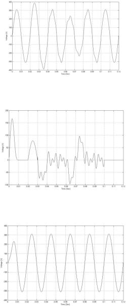
Reference Generation of Custom Power Devices (CPs) 109
current of phase 1. Load voltage and source current harmonics have been compensated satisfactory.
Figure 28. Source side voltage of phase 1
Figure 29. Compensator voltage of phase 1
Figure 30. Load side voltage of phase 1

110 An Update on Power Quality
Figure 31. Load side current of phase 1
Figure 32. Reactive current of phase 1
Figure 33. Harmonic current of phase 1
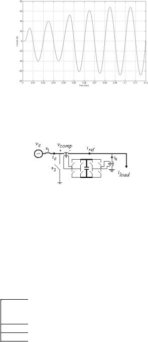
Reference Generation of Custom Power Devices (CPs) 111
Figure 34. Source side current of phase 1
7.3. Results of power flow control
For the investigation of the validity of the power flow control strategy in a distribution system, simulation of the test circuit of Figure 35 has been done.
Figure 35. General test system circuit
This power system consists of a harmonized and unbalanced three phase 20 kV (RMS, L-L), 50 Hz utility, a three phase balanced R-L load and a nonlinear three phase load. For the investigation of the voltage harmonic condition, utility voltages have harmonic and negative sequence components between 0.15 s and 0.35 s. Also, for the investigation of the proposed control strategy in unbalance condition, magnitude of the first phase voltage is increased to the 1.25 pu between 0.10 s and 0.20 s and decreased to the 0.75 pu between 0.3 s to 0.4 s. Investigation of the control circuit performance in fault condition is done by a three phase fault in output terminal of the main source between 0.4 s to 0.5 s. Table 4 shows the utility voltage harmonic and sequence parameters data and Table 5 shows the load power and voltage parameters. Table 6 show states of switches of s1 and s2 . A number of selected simulation results have been shown next.
Voltage |
Sequence |
Magnitude |
Phase |
Time |
order |
|
(pu) |
angle |
duration |
|
|
|
(degree) |
(sec) |
5 |
+ |
0.12 |
-45 |
0.15-0.35 |
3 |
- |
0.1 |
0 |
0.15-0.35 |
Table 4. Utility voltage harmonic and sequence parameters data
112 An Update on Power Quality
|
Load |
|
|
Nominal |
|
Nominal voltage |
|||
|
|
|
|
power (kVA) |
|
(RMS, L-L) |
|||
|
|
|
|
|
|
|
|
|
|
|
Linear |
|
50 |
|
20 kV |
||||
|
|
|
|
|
|
|
|
|
|
|
Non linear |
|
260 |
|
20 kV |
||||
|
|
|
|
|
|
|
|
||
Table 5. Load power and voltage parameters data |
|
|
|
||||||
|
|
|
|
|
|
|
|
||
|
switch |
|
0<t<0.4 sec |
|
0.4<t<0.5 sec |
||||
|
|
|
|
|
|
|
|
|
|
|
|
|
First |
|
Second |
|
First |
Second |
|
|
|
|
strategy |
|
strategy |
strategy |
strategy |
||
|
|
|
|
|
|
|
|
|
|
|
s1 |
|
close |
|
close |
|
open |
open |
|
|
|
|
|
|
|
|
|
|
|
|
s2 |
|
open |
|
open |
|
close |
close |
|
|
|
|
|
|
|
|
|
|
|
Table 6. States of switches
Figure 36, shows the source side voltage of phase 1. Figure 37, shows the compensator voltage of phase 1. Figure 38, shows the load side voltage of phase 1. Figure 39, shows the load side current of phase 1. Figure 40, shows the compensator current of phase 1. Figure 41, shows the source side current of phase 1. Figure 42, shows the load active and reactive powers. Figure 43, shows generation PAF active and reactive powers. Figure 44, shows the consumption active and reactive powers of the series active filter. Figure 45, shows generation active and reactive powers of the source. Figure 46, shows the difference between load voltage magnitude and nominal value and finally Figure 47, shows the difference between load voltage and source voltage phases.
Figure 36. Source side voltage of phase 1 (a swell has been occurred between 0.1 and 0.2 sec and a sag has been occurred between 0.3 and 0.4 sec. Also positive and negative harmonic sequences have been concluded between 0.15 and 0.35 sec. It has been tripped between 0.4 and 0.5 sec)
Reference Generation of Custom Power Devices (CPs) 113
Figure 37. Compensator voltage of phase 1 (compensator voltage has been determined for the sag, swell, interruption, negative sequence and harmonics improvement)
Figure 38. Load side voltage of phase 1 (swell, sag, positive and negative harmonic sequences have been improved. Load voltage has been compensated in the fault condition)
Figure 39. Load side current of phase 1 (it has different order harmonics. It should be considered that this current has been calculated after the voltage compensation, so the voltage unbalance has not been concluded in the current)

114 An Update on Power Quality
Figure 40. Compensator current of phase 1 (compensator current has been determined for the load current harmonics improvement as well as the reactive power)
Figure 41. Source side current of phase 1 (harmonics and reactive power components of the load current have been canceled)
Figure 42. Load active and reactive power (load is nonlinear resistive-inductive)
Reference Generation of Custom Power Devices (CPs) 115
Figure 43. Generation PAF active and reactive powers (reactive power and harmonics of load current have been supplied by the parallel active filter)
Figure 44. Consumption active and reactive power of series active filter (it is considered that the consumption power has been increased between sag times and decreased between swell times. Cause of power oscillation has been investigated in the text. Active power has been increased in fault condition for prevention of load interruption)
Figure 45. Generation active and reactive power of source (it is considered that the generation active power has been increased between sag times and decreased between swell times. Reactive power has been compensated. Cause of power oscillation has been investigated in the text. These powers are equal to zero in fault condition)
116 An Update on Power Quality
Figure 46. Difference between load voltage magnitude and nominal value (this amount is decreased by use of the PI controller to zero)
Figure 47. Difference between load voltage and source voltage phases (this amount decreased by use of PI controller to zero)
8. Conclusions
In this research different approaches for reference generation of UPQC have been proposed. Based on the general equations of Fourier transform, its response settling time is one cycle. In this research for increasing the response speed and improving the control system capabilities in dynamic conditions, very fast Fourier transform approach has been proposed for balanced three phase systems. In the proposed approach, settling time of the response could be reduced to one twelfth of a cycle. In the proposed approach, there were two data window lengths, T/12 and T/2. In the sag, swell, and load change conditions, control system was switched to T/12 for obtaining fast response. Then for improving the proposed approach responsibility in filtering of unwanted steady state oscillation, control system was switched to T/2 for obtaining no oscillated response. In these states, fast response in dynamic conditions as well as good response in the steady state conditions would be possible. In this research for the detection of the source voltage sag, swell, and load change conditions, derivative of the first order magnitude of the voltage and current signal, were compared to a constant value. This was based on the fact that in these conditions voltage or current magnitude generally changes rapidly. Proposed control approach was simulated in MATLAB/SIMULINK software. Voltage sag, swell, and harmonics were compensated by
Reference Generation of Custom Power Devices (CPs) 117
SAF. But, reactive power and current harmonics were compensated by PAF. THD of load voltage before compensation was 14.14 percent which was reduced to almost zero after the compensation. But, THD of the source current before compensation was 9 percent which was reduced to almost zero after the compensation.
Also the proposed reference generation algorithm based on MOADALINE has been compiled in MATLAB software via M-File. Voltage harmonics have been compensated by SAF of the UPQC and current harmonics have been compensated by PAF of the UPQC. Based on the results proposed strategy not only could generate pure sinusoidal source current and load voltage but also could compensate source reactive power satisfactory. Total harmonic distortion of load voltage and current before compensation was 0.17 and 0.12 respectively which was reduced to almost zero after the compensation.
Another scope of this research was reference generation based on power flow control. This approach was based on relation between active and reactive powers and load voltage. In this approach amount of reactive power arranged to zero but amount of active power arranged to load nominal power. Also a PI controller used for arranging the load voltage magnitude to the nominal amount.
Author details
Ahad Mokhtarpour
Department of Electrical Engineering, Tabriz Branch, Islamic Azad University, Tabriz, Iran
Heidarali Shayanfar
Department of Electrical Engineering, South Tehran Branch, Islamic Azad University, Tehran, Iran
Seiied Mohammad Taghi Bathaee
Department of Electrical Engineering, K.N.T University, Tehran, Iran
9. References
[1]Fujita H., Akagi H. The Unified Power Quality Conditioner: The Integration of Series and Shunt Active Filters. IEEE Transaction on Power Electronics 1998; 13(2) 315-322.
[2]Hannan M. A., Mohamed A. PSCAD/EMTDC Simulation of Unified Series-Shunt Compensator for Power Quality Improvement. IEEE Transaction on Power Delivery 2005; 20(2) 1650-1656.
[3]Shayanfar H. A., Mokhtarpour A. Management, Control and Automation of Power Quality Improvement. In: Eberhard A. (ed.) Power Quality. Austria: InTech; 2010. p127-152.
[4]Khadkikar V., Chandra A. A Novel Structure for Three Phase Four Wire Distribution System Utilizing Unified Power Quality Conditioner (UPQC). IEEE Transactions on Industry Applications 2009; 45(5) 1897-1902.
[5]Kwan K.H., Chu Y.C., So P.L. Model-Based H∞ Control of a Unified Power Quality Conditioner. IEEE Transactions on Industrial Electronics 2009; 56 (7) 2493-2504.
118An Update on Power Quality
[6]Khadkikar V., Chandra A. A New Control Philosophy for a Unified Power Quality Conditioner (UPQC) to Coordinate Load-Reactive Power Demand Between Shunt and Series Inverters. IEEE Transactions on Power Delivery 2008; 23 (4) 2522-2534.
[7]Lee W.C., Lee D.M., Lee T.K. New Control Scheme for a Unified Power Quality Compensator-Q with Minimum Active Power Injection. IEEE Transactions on Power Delivery 2010; 25(2) 1068-1076.
[8]Han B., Bae B., Kim H., Baek S. Combined Operation of Unified Power-Quality Conditioner with Distributed Generation. IEEE Transaction on Power Delivery 2006; 21(1) 330-338.
[9]Mohammadi H.R., Varjani A.Y., Mokhtari H. Multiconverter Unified Power-Quality Conditioning System: MC-UPQC. IEEE Transactions on Power Delivery 2009; 24(3) 1679-1686.
[10]Mokhtarpour A., Shayanfar H.A., Bathaee. S.M.T Extension of Fourier Transform for Very Fast Reference Generation of UPQC. International Journal on Technical and Physical Problems of Engineering 2011; 3(4) 120-126.
[11]Mokhtarpour A., Shayanfar H.A., Bathaee. S.M.T UPQC Control Based on MOADALINE Approach. International Journal on Technical and Physical Problems of Engineering 2011; 3(4) 115-119.

Section 3
Power Quality Improvement in End Users Stage

Chapter 7
Power Quality Improvement Using
Switch Mode Regulator
Raju Ahmed and Mohammad Jahangir Alam
Additional information is available at the end of the chapter
http://dx.doi.org/10.5772/53234
1. Introduction
Power quality describes the quality of voltage and current. It is an important consideration in industries and commercial applications. Power quality problems commonly faced are transients, sags, swells, surges, outages, harmonics and impulses [1]. Among these voltage sags and extended under voltages have large negative impact on industrial productivity, and could be the most important type of power quality variation for many industrial and commercial customers [1-5].
Voltage sags is mainly due to the fault occurring in the transmission and distribution system, loads like welding and operation of building construction equipment, switching of the loaded feeders or equipments. Both momentary and continuous voltage sags are undesirable in complex process controls and household appliances as they use precision electronic and computerized control.
Major problems associated with the unregulated long term voltage sags include equipment failure, overheating and complete shutdown. Tap changing transformers with siliconcontrolled rectifiers (SCR) are usually used as a solution of continuous voltage sags [6]. They require large transformer with many SCRs to control the voltage at the load which lacks the facility of adjusting to momentary changes. Some solutions have been suggested in the past to encounter the problems of voltage sag [7-11]. But these proposals have not been realized practically to replace conventional tap changing transformers.
Now a day’s various power semiconductor devices are used to raise power quality levels to meet the requirements [12]. Several AC voltage regulators have been studied as a solution of voltage sags [13-18]. In [13] the input current was not sinusoidal, in [14-16] the efficiency of the regulator was not analyzed and in [17-18] the input power factor was very low and the efficiency is also found poor. Compact and fully electronic voltage regulators are still unavailable practically.
122 An Update on Power Quality
Dynamic Voltage Restorer (DVR) is sometimes used to regulate the load side voltage [1921]. The DVR requires energy storage device to compensate the voltage sags. Flywheels, batteries, superconducting magnetic energy storage (SMES) and super capacitors are generally used as energy storage devices. The rated power operation of DVR depends on the size and capacity of energy storage device which limits its use in high power applications. Whereas, switching regulator needs no energy storage devices, therefore, can be used both in low power and high power applications.
The objective of this chapter is to describe the operation and design procedure of a switch mode AC voltage regulator. Firstly, some reviews of the regulators are presented then the procedure of design and analysis of a switch mode regulator is described step by step. Simulation software OrCAD version 9.1 [22] is used to analyze the regulator. The proposed regulator consists mainly two parts, power circuit and control circuit. The power circuit consist two bi-directional switches which serve as the freewheeling path for each other. A signal generating control circuit is to be associated with the power circuit for getting pulses of the switches. In the control circuit, a commercially available pulse width modulator IC chip SG1524B is used, thus circuit is compact and more viable.
2. Review of voltage regulators
2.1. Switching-mode power supply (SMPS)
A switching-mode power supply (SMPS) is switched at very high frequency. Conversion of both step down and step up of voltage is possible using SMPS. Uses of SMPSs are now universal in space power applications, computers, TV and industrial units. SMPSs are used in DC-DC, AC-AC, AC-DC, DC-AC conversion for their light weight, high efficiency and isolated multiple outputs with voltage regulation. Main parts of a Switching-mode power supply are:
(a) Power circuit, (b) Control circuit.
Figure 1 shows the block diagram of a SMPS. The power circuit is mainly the input, output side with the switching device. The switching device is continuously switched at high frequency by the gate signal from the control circuit to transfer power from input to the output. The control circuit of a SMPS basically generates high frequency gating pulses for the switching devices to control the output voltage. Switching is performed in multiple pulse width modulation (PWM) fashion according to feedback error signal from the load. High frequency switching reduces filter requirements at the input and output sides of the converter. Simplest PWM control uses multiple pulse modulations generated by comparing a DC with a high frequency carrier triangular wave.
The PWM control circuit is commonly available as integrated form. The designer can select the switching frequency by choosing the value of RC to set oscillator frequency. As a rule of thumb to maximize the efficiency, the oscillation period should be about 100 times longer than the switching time of the switching device such as Transistor, Metal oxide semiconductor field-effect transistor (MOSFET), Insulated gate bipolar transistor (IGBT). For
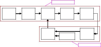
Power Quality Improvement Using Switch Mode Regulator 123
example, if a switch has a switching time of 0.5 us, the oscillator period would be 50 us, which gives the maximum oscillation frequency of 20 KHz. This limitation is due to the switching loss in the switching devices. The switching loss of switching devices increases with the switching frequency. In addition, the core loss of inductor limits the high frequency operation.
Power circuit
Input |
Input |
Switch |
Output |
Output |
|
filter |
filter |
||||
|
|
|
|||
|
|
Gating |
|
Feed back |
|
|
|
Signal |
Reference |
Control |
|
|
|
Generator |
Voltage |
Circuit |
Control circuit
Figure 1. Block diagram of Switching-mode power supply (SMPS).
2.2. DC-DC converter
Figure 2 illustrates the circuit of a classical linear power converter. Here power is controlled by a series linear element; either a resister or a transistor is used in the linear mode. The total load current passes through the series linear element. In this circuit greater the difference between the input and the output voltage, more is the power loss in the controlling device (linear element). Linear power conversion is dissipative and hence is inefficient.
The circuit of Fig. 3 illustrates basic principle of a DC-DC switching-mode power converter. The controlling device is a switch. By controlling the duty cycle, (the ratio of the time in on positions to the total time of on and off position of a switch) the power flow to the load can be controlled in a very efficient way. Ideally this method is 100% efficient. In practice, the efficiency is reduced as the switch is non-ideal and losses occur in power circuits. Hence, one of the prime objectives in switch mode power conversion is to realize conversion with the least number of components having better efficiency and reliability. The DC output voltage to the load can be controlled by controlling the duty cycle of the rectangular wave supplied to the base or gate of the switching device. When the switch is on, it has only a small saturation voltage drop across it. In the off condition the current through the switch is zero.
The output of the switch mode power conversion circuit (Fig. 3) is not pure DC. This type of output is applicable in some cases such as oven heating without proper filtration. If constant DC is required, then output of converter has to be smoothed out by the addition of low-pass filter.
124 An Update on Power Quality
|
|
|
|
|
|
|
|
R1 |
V |
||
|
|
|
|
|
|
|
|
|
|
|
V |
+ |
|
|
|
|
|
|
Vin |
|
Vout |
|
R2 |
|
|
|
|
|
|
||||||
|
|
|
|
|
|
|
|
||||
|
|
_ |
|
|
|
|
|
||||
|
|
|
Vout |
||||||||
|
|
|
|
|
|
|
|
|
|
|
|
|
|
|
|
|
|
|
|
|
|
|
|
t
Figure 2. Linear (dissipative) DC-DC power conversion circuit.
V |
Vout |
|
|
|
|
|
|
|
|
|
|
Vin |
|
|
BJT |
|
|
|
|
|
|
||||
|
|
|
|
||||||||
+ |
|
|
|
|
|
|
|
|
|
R |
|
|
|
|
|
|
|
|
|
|
|||
Vin |
|||||||||||
_ |
|||||||||||
|
|
|
|
|
|
|
|
|
Vout |
||
|
|||||||||||
|
|||||||||||
|
|
|
|
|
|
|
|
|
|
|
|
Figure 3. Switching-mode (non dissipative) DC-DC power conversion circuit.
2.2.1. Types of DC-DC converter
There are four basic topologies of switching DC-DC regulators:
a.Buck regulator
b.Boost regulator
c.Buck-Boost regulator and
d.Cûk regulator.
The Circuit diagram of four basic DC-DC switching regulators is shown in Fig. 4. The expression of output voltage for the four types of DC-DC regulators are as follows:
For Buck regulator, Vout |
kVin , For Boost regulator, Vout |
|
Vin |
|||||
1 |
k |
|||||||
|
|
|
|
|
|
|||
For BuckBoost regulator and Cûk regulator, Vout |
|
-kVin |
|
|
|
|||
1 k |
|
|
||||||
|
|
|
|
|
||||
Where k is the duty cycle, the value of k is less than 1. For Buck regulator output voltage is always lower than input voltage, for Boost regulator output voltage is always higher than input voltage. For Buck-Boost regulator and Cûk regulator output voltage is higher than input voltage when the value of k is higher than 0.5, and output voltage is lower than input voltage when the value of k is lower than 0.5. When k is equal to 0.5 output voltage is same

Power Quality Improvement Using Switch Mode Regulator 125
as input voltage. In Buck-Boost and Cûk regulator, the polarity of output voltage is opposite to that of the input voltage, therefore theses regulators are also called inverting regulators.
+ |
BJT |
|
L |
|
|
L |
D |
|
Vg |
|
|
R |
+ |
BJT |
C |
R |
|
|
|
C |
||||||
|
|
|
||||||
_ |
Vin |
D |
Vout |
_ |
Vin Vg |
|
Vout |
|
|
|
|
|
|
|
|
(a) Buck regulator |
|
|
|
|
(b) Boost regulator |
|
|
BJT |
|
D |
|
|
|
L1 |
L2 |
|
|
|
|
|
|
C1 |
|
||
+ |
Vg |
C |
|
R |
+ |
Vg |
BJT D C2 |
R |
_ Vin |
L |
Vout |
|
|||||
|
|
|
_ Vin |
|
Vout |
|||
(c) Buck-Boost regulator |
|
|
|
|
(d) Cûk regulator |
|
||
Figure 4. Circuit diagram of DC-DC regulator, (a) Buck regulator, (b) Boost regulator, (c) Buck-Boost regulator, (d) Cûk regulator.
2.3. AC-AC converter
The AC voltage regulator is an appliance by which the AC output voltage can be set to a desired value and can be maintained constant all the time irrespective of the variations of input voltage and load. This subject is vast and the field of application extends from very large power systems to small electronic apparatus. Naturally, the types of regulators are also numerous. The design of the regulators depends mainly on the power requirements and degree of stability.
The AC voltage can be regulated by the following ways.
a.Solid-state tap changer and steeples control by variac
b.Solid-tap changer using anti-parallel SCRs
c.Voltage regulation using servo system
d.Phase controlled AC regulator
e.Ferro-resonant AC regulator
f.Switch mode AC regulator
2.3.1. Solid-state tap changer and stepless control by variac
The voltage regulations by tap-changing switches are used in many industrial applications where the maintenance of output voltage at a constant value is not very stringent, such as ordinary battery chargers, electroplating rectifiers etc. For smaller installation, off-load tap
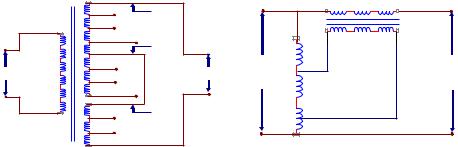
126 An Update on Power Quality
changing switches are used and for large installation on-load tap changing switches are used. The switches are generally incorporated at the secondary of the transformer. For a low voltage high current load, the switches are provided on the primary side of the transformer due to economical reason. For line voltage correction, taps are provided on the primary of the transformer. For three-phase transformers three pole tap changing switches are used.
In off-load tap changer, the output is momentarily cut-off from the supply. It is therefore used for low capacity equipment and where the momentary cut-off of the supply is not objectionable for the load. The major limitation of the off-load tap changing switches is the occurrences of arcs at the contact points during the change-over operation. This shortens the life of off-load rotary switches, particularly of high current ratings. In Fig. 5 (a), three fourposition switches of an off load tap changer are shown, such that the minimum of X volts per step are available at the output.
The voltage is corrected by tap-charging switches in steps. Where stepless control is required, variable autotransformers or variacs are used. The normal variac consists of a toroidal coil wound on a laminated iron ring. The insulation of the wire is removed from one of the end faces and the wire is grounded to ensure a smooth path for the carbon brush. Carbon brush is used to limit the circulating current, which flows between the short-circuited turns.
A Buck-Boost transformer is sometimes used for AC voltage regulation when the output voltage is approximately the same as the mean input voltage as shown in Fig. 5(b). In this case if the output voltage is less than or greater than the desired value, it can be increased or decreased to the desired value by adding a suitable forward or reverse voltage with the input through the Buck-Boost transformer.
|
16X |
|
|
|
Ns |
|
|
Coarse |
|
|
|
|
|
|
16X |
|
|
|
|
|
|
|
|
|
|
|
|
|
16X |
|
|
|
Np |
|
|
4X |
Medium |
|
|
Buck – Boost |
Output |
|
|
|
Input |
Transformer |
||
Input |
4X |
|
Output |
|
= Ei Ei/2 |
|
|
= Ei |
|
||||
|
4X |
|
|
Ei/2 |
(Ns/Np) |
|
|
|
|
|
|
||
|
|
|
|
|
|
|
|
X |
Fine |
|
|
|
|
|
X |
|
|
|
|
|
|
|
|
|
|
|
|
|
X |
|
|
|
|
|
(a) Off load tap changing switch |
|
(b) Voltage control by combination of a |
||||
|
arrangement. |
|
|
Buck–Boost transformer and a variac. |
||
Figure 5. Circuit diagram of AC voltage controller using (a) Off load tap changer and (b) Buck-Boost transformer and variac.
2.3.2. Solid tap changer using anti-parallel SCRs
Anti-parallel SCRs combinations can replace the voltage sensitive relay in the tap-changing regulator. Figure 6 shows a tap changer with three taps which can be connected to the load
Power Quality Improvement Using Switch Mode Regulator 127
through three anti-parallel switches. When the SCR1-SCR2 switch is fired, tap 1 is connected to the load. Similarly taps 2 and 3 can be connected to the load through the SCR3-SCR4 and CSR5-SCR6 switches respectively. Thus, any number of taps can be connected to the load with similar SCR switches. When one group of SCRs operates for the whole cycle and other groups are off, the voltage corresponding to the tap of that group appears at the load. Changeover from one loop to the other is done simply by shifting the firing pulses from one group of SCRs to the other.
With resistive load, the load current becomes zero and the SCRs stop conduction as soon as the voltage reverses its polarity. Therefore, when one group is fired, the other groups are commutated automatically. With reactive loads, the situation is complicated by the fact that the zero current angle depends on the load power factor. This means that the SCR conducts a finite value of current at the time of reversal of line voltage. This results in either preventing a tap change due to reverse bias on the SCR to be triggered or causing a short circuit between the taps through two SCRs.
2.3.3. Voltage regulation using servo system
Voltage regulators using servo systems are quite common. Both single and three-phase types are available. The rating of this type of regulator is quite high and is more economical for high power rating. This regulator normally consist a variac driven by a servomotor, a sensing unit and a voltage and power amplifier to drive the motor in a reversible way. Various types of driving motor may be used for regulating the unit, such as direct current, induction and synchronous motors. However, in all cases, the motor must come to rest rapidly to avoid overrun and hunting. The amount of overrun may be reduced by dynamic braking in the case of a DC motor or by disconnecting the motor from the variac by a clutch as soon as the signal from the measuring unit ceases. The main disadvantage of this type of regulator is the low life of the contact points of the relays.
2.3.4. Phase controlled AC voltage regulator
Voltage regulators using SCRs are quit common. The load voltage is regulated by controlling the firing instants of the SCRs. There are various circuits for single phase and three phase regulators using SCRs. Though the output voltage can be precisely controlled by this method, the harmonic introduced in the load voltage are quit large and this circuit is used for applications where the output voltage waveform need not be strictly sinusoidal. The circuit arrangement for a single phase SCR regulator is shown in Fig. 6 and Fig. 7.
2.3.5. Ferro-resonant AC voltage regulator
The concept of the stabilization of AC voltage using a saturated transformer is rather old. The basic circuit arrangement consists of a linear reactor or transformer T1 and a nonlinear saturated reactor or transformer T2 connected in series as shown in Fig. 8. Since the two elements T1 and T2 are in series, the current through them is the same. Transformer T2 is operated under saturated. The voltage division between the two is according to their
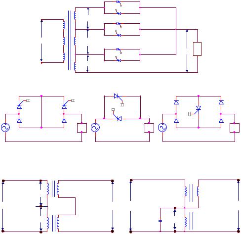
128 An Update on Power Quality
impedances. Due to nonlinear characteristics of T2 the percentage change of voltage across it is much smaller compared to the percentage change of input voltage. If a suitable voltage proportional to the current is subtracted from the voltage across T2 a practically constant output voltage can be obtained. The circuit arrangement shown is Fig. 8(a) has some drawbacks such as, no load input current is high, and good output voltage stability cab be achieved only at a particular load. Hence some modifications are necessary to improve its performance. The major modification is to place a capacitor across the saturated transformerT2 that is shown in Fig. 8(b).
|
SCR 1 |
GR 1 |
|
SCR 2 |
|
|
V1 |
|
|
SCR 3 |
|
|
SCR 4 |
GR 2 |
Input |
V2 |
Lo |
|
||
|
SCR 5 |
Output ad |
|
|
|
|
SCR 6 |
GR 3 |
|
V3 |
|
Figure 6. Circuit diagram of solid tap changer using anti-parallel SCRs.
|
SCR2 |
SCR1 |
|
|
SCR1 |
SCR2 |
|
|
|
|
|
|
|
|
SCR1 |
|
Input |
Output |
|
Input |
Output |
Input |
Output |
|
(a) |
(b) |
(c) |
Figure 7. Phase controlled AC voltage regulator, (a) Using back to back SCR and diode and (b) using inverse parallel SCR (c) Using diode-bridge and single SCR
ET |
T 1 |
|
ET1(P) |
ET1(S) |
|
|
|||
Input |
Output |
Input |
|
Output |
ET |
T 2 |
C |
ET2 |
|
|
|
|
||
|
|
|
|
(a) |
(b) |
Figure 8. Fero-resonant AC voltage regulator. |
|
The value of the capacitor is such that it resonant with the saturated inductance of T2 at some point. The characteristics of the circuit is such that a small change in voltage across T2
Power Quality Improvement Using Switch Mode Regulator 129
causes the circuit to go out of resonance consequently a large change in input current and power factor. For a change in the input voltage, the change in voltage across the resonant circuit is small but the change in voltage at T1 is large, and by suitable proportioning of the voltage, a good degree of stabilization is achieved for the variation of input voltage as well as load current. The simple Ferro-resonant regulator has the following disadvantages:
a.The output voltage changes with frequency.
b.Since the core operates in saturation and output is derived from the tank circuit, the core volume is large, the core losses are high and external magnetic field is also high.
2.3.6. Switch mode AC voltage regulator
In switch mode AC voltage regulator, the switching devices are continuously switching on and off with high frequency in order to transfer energy from input to output. The high operating frequency results in the smaller size of the switch mode power supplies since the size of power transformer inductors and filter capacitors is inversely proportional to the frequency. The SMPS are more complicated and more expensive, their switching current can cause noise problems, and simple designs can have a poor power factor.
Four common types of switch mode converters are used in DC-DC conversion. They are Buck, Boost, Buck-Boost and C^UK converters. Researches are trying to modify these DC regulators to regulate AC voltages. BuckBoost and Cûk converter configuration has been investigated for voltage regulation [17-18]. But in every case it is found that the input power factor is very low and the efficiency is poor.
3. Design and analysis of switching-mode AC voltage regulator
3.1. Operation principle of switching-mode AC voltage regulator
3.1.1. Operation of power circuit
Voltage sag is an important power quality problem, which may affect domestic, industrial and commercial customers. Voltage sags may either decrease or increase in the magnitude of system voltage due to faults or change in loads. Momentary and sustained over voltage and under voltage may cause the equipment to trip out, which is highly undesirable in certain application. In order to maintain the load voltage constant in case of any fluctuation of input voltage or variation of load some regulating device is necessary.
In this chapter the principle of operation of high frequency switching AC voltage regulator, design of its filter circuit and snubber circuit are described. Performance of the regulator is also analyzed using simulation software OrCAD version 9.1. Switch-mode power supplies (SMPS) incorporate power handling electronic components which are continuously switching on and off with high frequency in order to provide the transfer of electric energy from input to output. The design of AC voltage regulator depends on power requirement, degree of stability and efficiency. Solid state AC regulator using phase control technique are not new and are widely used in many application such as heating and lighting control etc.

130 An Update on Power Quality
These regulators are not suited for critical loads because the output waveforms are truncated sine waves, which contain large percentage of distortion. The input power factor is low. These drawbacks are largely overcome and the voltage can be efficiently controlled by means of a solid-state AC regulator using PWM technique.
The power circuit of the proposed AC voltage regulator is shown in Fig. 9. The circuit operation can be explained with the help of Fig. 10. During positive half cycle of the input voltage, at mode 1, when switch-1 is on and switch-2 is off, the current passes through diode D1, switch-1, diode D4 and through the inductor and the energy is stored in the inductor. At mode 2, when switch-1 is off and switch-2 is on, the energy stored in the inductor is transferred through diode D8, switch-2 and diode D5. At mode 1, power is transferred from source and at mode 2, power is not transferred from the source, so by controlling the on and off duration of switch-1 output power can be controlled.
During negative half cycle of the input voltage, at mode 1, when switch-1 is on and switch-2 is off the current passes through the inductor, diode D3, switch-1, and diode D2 and the energy is stored in the inductor. At mode 2, when switch-1 is off and switch-2 is on the energy stored in the inductor is transferred through diode D6, switch-2 and diode D7.
|
|
D1 |
|
|
D3 |
|
|
||||||||
|
|
|
|
|
|
||||||||||
|
|
Gate signal 1 |
|
|
|
|
|
||||||||
|
|
|
|
|
|
|
|||||||||
|
|
|
|
|
|
|
|
|
|
+ |
+ |
|
|
|
|
|
|
|
|
|
|
|
|
|
|
- |
|
Switch 1 |
|
||
|
|
|
|
|
|
|
|
|
|
- |
|
|
|||
|
|
|
|
|
|
|
|
|
|
|
|
|
|
|
|
|
|
|
|
|
|
|
|
|
|
|
|
|
|
|
|
|
|
|
|
|
|
|
|
|
|
|
|
|
|
|
|
D2 |
0 |
D4 |
D5 |
Gate signal 2 |
D6 |
TX1 |
|
|
|
|
|
|
0 |
+ - |
Switch 2 |
|
Lo |
+ - |
|
|
||
|
|
ad |
||
|
|
|
|
|
D7 |
|
|
D8 |
0 |
0
Figure 9. Power circuit of the proposed AC voltage regulator.
Switch 1 |
|
Mode 1, current path |
|
Switch 2 |
L |
|
|
Mode 2, current path |
|
(a) |
|
Switch 1 |
|
Mode 1, current path |
|
Switch 2 |
L |
|
|
Mode 2, current path |
|
(b) |
|
Figure 10. Operation of the power circuit of AC voltage regulator (a) Operation during positive half cycle (b) Operation during negative half cycle
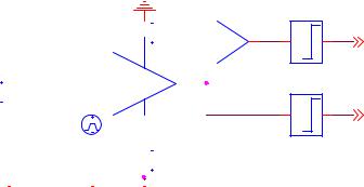
Power Quality Improvement Using Switch Mode Regulator 131
3.1.2. Operation of control circuit
The gate signal generating circuit for a manually controlled AC voltage regulator is shown in Fig. 11. The control circuit incorporates an Operational Amplifier (OPAMP) whose positive input is a variable DC voltage V1, and negative input is a fixed saw-tooth signal V2. In this circuit the OPAMP acts as a comparator, output of the OPAMP depends on the difference of the two inputs. The negative input (saw-tooth wave) is kept constant and positive input (DC voltage) is varied. So output pulse width depends on DC input voltage of OPAMP i.e. when DC input is higher the output of comparator will be wider and when DC input is lower the output of comparator will be narrower.
The outputs of OPAMP are used to turn on/off the switches of the power circuit of the regulator to regulate the output voltage. The output of OPAMP is directly passed through limiter-1 which is the gate signal for switch-1 and after inverting the output of the comparator is passed through the limiter-2 which is the gate signal for switch-2. The function of the limiter is to limit the output of comparator from 0 to 5 V. When switch-1 of the power circuit is on then switch-2 should be off. So the gate signal generating circuit is arranged in such a way that when gate signal of switch-1 is on then gate signal for switch-2 is off and vice versa.
|
|
|
|
|
|
|
|
|
|
|
|
|
3 |
+ |
|
|
|
|
|
|
|
|
V1 |
|
|
||||||
|
|
|
|
|
|
|
2 |
||||||||
|
|
|
|
|
|
|
- |
||||||||
|
|
|
|
|
|
|
|
V1 = 10 |
|
||||||
|
|
|
|
|
|
|
|
|
|||||||
|
|
|
|
|
|
|
|
|
|||||||
|
|
|
|
|
|
|
|
|
|||||||
|
|
|
|
|
|
|
|
|
|
|
|||||
5Vdc |
|
V2 |
|||||||||||||
|
|
|
|
V2 = 0 |
|
|
|
|
|||||||
|
|
|
|
|
|
|
|
TD = 0 |
|
|
|
||||
|
|
|
|
|
|
|
|
TR = .125ms |
|
|
|
|
|||
|
|
|
|
|
|
|
|
TF = .125ms |
|
|
|
|
|||
|
|
|
|
|
|
|
|
PW = .005ms |
|
|
|
|
|||
|
|
|
|
|
|
|
|
PER = .255ms |
|
|
|
|
|||
|
|
|
|
|
|
|
|
|
|
|
|
|
|
|
|
|
|
|
|
|
0 |
|
|
|
|
0 |
|
||||
0
|
|
|
|
|
|
V3 |
|
|
|
|
|
|
|
|
|
|
|
|
|
|
|
|
|
|
|
|
|
|
|
8 |
|
|
|
12Vdc |
|
||||
|
|
|
|
|
|
|
|||
|
|
V+ |
OUT |
1 |
|
||||
|
|
|
|||||||
|
|
|
|
|
|||||
|
|
V- |
|
|
|
||||
|
|
|
|
|
|
|
|
||
4 |
|
AD648A |
|
||||||
|
|
||||||||
|
|
|
V4 |
|
|
|
|||
|
|
|
|
|
|
|
|
|
|
|
|
|
|
|
|
12Vdc |
|
||
|
|
|
|
|
|
|
|||
|
|
|
|
|
|
|
|||
|
|
|
|
|
|
|
|
|
|
|
|
|
|
0 |
|
|
|
||
5 -1
0
gate signal 2
5
0
gate signal 1
Figure 11. Gate signal generation circuit of manually controlled AC voltage regulator.
3.2. Manually controlled AC voltage regulator
When the stability is not very stringent, manually controlled AC voltage regulator is generally preferred from economic considerations.
The basic circuit of a manually controlled AC voltage regulator is shown in Fig. 12. When any change in output voltage occurs due to change in input voltage or change in load, the voltage can be regulated to the desirable value by changing the DC voltage of the gate signal generating circuit manually. The power circuit of the proposed regulator shown in Fig. 12 is implemented using ideal switches; later part of this chapter the ideal switches is replaced by practical switches. The regulator proposed in this chapter is employed to regulate the output
132 An Update on Power Quality
voltage to 300V (peak) for variations of input voltage from 200V (peak) to 400V (peak), also for variation of load from 100 ohm to 200 ohm. However, the output voltage can be set to any desirable value according to requirement. The values of all voltages and currents indicated in this chapter are in peak values.
The input current and output voltage waveforms of the manually controlled AC voltage regulator as shown in Fig. 12, is shown in Fig. 13, when the input voltage is 300V and output voltage is also 300V. The spectrum of the input current and output voltage as shown in Fig. 13 is shown in Fig. From the waveforms it is seen that the waveforms are not smooth, sinusoidal and from the spectrum it is seen that due to high frequency switching the significant number and amount of harmonics occur. The switching frequency is selected to 4 KHz. Harmonics occurs at switching frequency and its odd multiple frequencies. So, filters are required at input and output side to filter out these harmonics to get desired sinusoidal waveforms.
SW1 |
S1 |
|
|
|
|
|
|
|
|
|
|
|
|
|
|
+ |
+ |
|
|
|
|
|
|
- |
- |
|
|
|
|
|
|
0 |
|
|
|
|
|
|
+ - |
Input |
|
|
|
|
|
0 |
|
|
|
|
|
|
+ - |
||
VOFF = 0 |
|
|
|
|
|
|
|
VAMPL = 300 |
|
|
|
|
|
|
|
FREQ = 50 |
|
|
|
|
|
|
|
|
|
|
|
|
|
0 |
|
|
|
|
|
|
|
0 |
|
|
|
|
|
|
8 |
V3 |
|
|
|
|
|
|
|
|
|
|
|
|
3 |
+ |
V+ |
12Vdc |
|
|
|
|
|
|
|||
|
|
|
|
|
|
1 |
|
5Vdc |
|
|
|
|
|
OUT |
|
|
|
|
|
|
|
||
V1 |
|
|
2 |
- |
V- |
|
|
V1 = 10 |
V2 |
|
|
|
|||
|
|
|
AD648A |
||||
V2 = 0 |
|
|
|
|
|||
TD = 0 |
|
|
|
4 |
V4 |
|
|
TR = .125ms |
|
|
|
|
|
||
TF = .125ms |
|
|
|
|
12Vdc |
|
|
PW = .005ms |
|
|
|
|
|
||
PER = .255ms |
|
|
|
|
|
|
|
0 |
|
0 |
|
|
|
0 |
|
SW2 |
TX1 |
S2 |
R6 |
|
100 |
 0
0
|
5 |
|
|
|
|
|
|
|||
-1 |
|
|
|
|
|
|
|
|
||
|
|
|
|
|
|
|
|
|
|
|
|
0 |
|
|
|
|
SW2 |
||||
|
|
|
|
|
|
|
|
|
||
|
|
|
|
|
|
|
|
|
||
5 |
|
0 |
SW1 |
|
Figure 12. Fundamental circuit of manually controlled AC voltage regulator (ideal switch implementation).
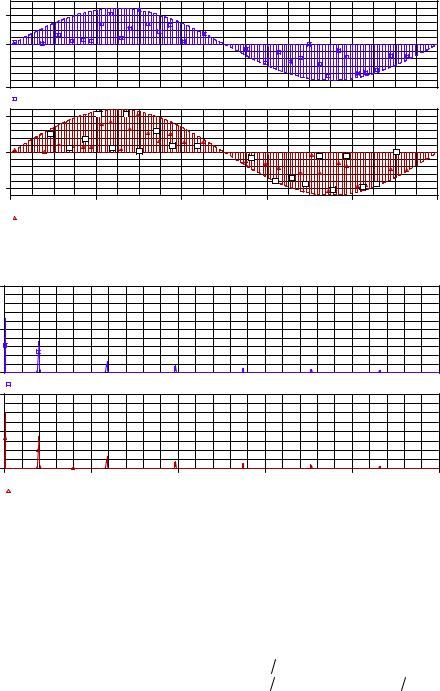
Power Quality Improvement Using Switch Mode Regulator 133
10A |
|
|
|
|
|
0A |
|
|
|
|
|
SEL>> |
|
|
|
|
|
-15A |
- I(V5) |
|
|
|
|
|
|
|
|
|
|
500V |
|
|
|
|
|
0V |
|
|
|
|
|
-500V |
|
|
|
|
|
0s |
4ms |
8ms |
12ms |
16ms |
20ms |
|
V2(R3) |
|
Time |
|
|
|
|
|
|
|
Figure 13. Input current and output voltage waveforms of the regulator shown in Fig. 12. -I(V5): Input current, V(R3:2): Output voltage.
10A |
|
|
|
|
|
5A |
|
|
|
|
|
0A |
- I(V5) |
|
|
|
|
400V |
|
|
|
|
|
|
|
|
|
|
|
200V |
|
|
|
|
|
SEL>> |
|
|
|
|
|
0V |
10KHz |
20KHz |
30KHz |
40KHz |
50KHz |
0Hz |
|||||
|
V2(R3) |
Frequency |
|
|
|
|
|
|
|
||
Figure 14. Spectrum of input current and output voltage waveforms. -I(V5):Input current V(R3:2): Output voltage.
3.3. Filter design
3.3.1. Output filter design
For getting smooth output voltage, a low pass LC filter of proper L and C value is needed at the output of this regulator. The output filter circuit and the corresponding AC sweep are
shown in Fig. 15. From this circuit we can write, V |
Vin J |
C |
or |
V0 |
|
1 |
J( L-1 |
C) |
|
C( L-1 C) |
|||
0 |
|
Vin |
||||
|
|
|
|
|
|
|
134 An Update on Power Quality
The input to the filter is high frequency modulated 50 Hz AC input. The switching signal that modulates the 50 Hz signal is taken to be 4 KHz in this case. So, we will have to make a filter that would pass signal up to 1 KHz (say) and attenuate all other frequencies. This would result a nearly sinusoidal output voltage. In the LC filter section we choose a capacitor of 5µF and determine the value of inductor for a cutoff from AC sweep analysis through OrCAD simulation. We found the value of the inductor to be 30 mH.
|
L1 |
|
|
500V |
|
|
|
|
30mH |
|
|
|
|
|
|
300Vac |
Input |
C1 |
R1 |
250V |
|
|
|
0Vdc |
|
5u |
100 |
|
|
|
|
|
|
|
|
|
|
||
|
|
|
|
0V |
100Hz |
1.0KHz |
10KHz |
|
|
|
0 |
10Hz |
|||
|
|
|
V(R1:2) |
|
|
||
|
|
|
|
|
|
||
|
|
(a) |
|
|
Frequency |
|
|
|
|
|
|
(b) |
|
|
|
Figure 15. Output voltage filter and AC sweep analysis (a) Output voltage filter (b) AC sweep analysis.
3.3.2. Input filter design
A low pass LC filter of proper L and C value is needed at the input of the regulator to filter out some of the harmonics from the supply system. The input filter circuit and the corresponding AC sweep are shown in Fig. 16. Input current contains harmonics at switching frequency 4 KHz and its odd multiple. In order to remove harmonics above 1 KHz, we choose a capacitor of 5µF and determine the value of inductor for a cutoff from AC sweep analysis through OrCAD simulation. We found the value of the inductor to be 30 mH.
L1 |
|
20A |
|
|
|
30mH |
|
|
|
|
|
|
|
|
|
|
|
20Aac |
R1 |
10A |
|
|
|
0Adc |
|
|
|
||
Input |
C1 |
|
|
|
|
|
|
|
|
|
|
|
5u |
0A |
|
|
|
|
|
100Hz |
1.0KHz |
10KHz |
|
|
0 |
10Hz |
|||
|
- |
I(R2) |
|
|
|
|
|
|
|
||
|
|
|
Frequency |
|
|
|
(a) |
|
(b) |
|
|
Figure 16. Input current filter and corresponding AC sweep analysis (a) Input current filter (b) AC sweep analysis.
Power Quality Improvement Using Switch Mode Regulator 135
3.4. Free wheeling path and surge voltage across switching devices
The power circuit of the proposed regulator with input and output filter is shown in Fig. 17. In an inductor, current does not change instantaneously. When the switches of power circuit switched on and off the current into the inductor of input and output filter are changed abruptly. Abrupt change of current causes a high di/dt resulting high voltage which is equal to Ldi/dt. These voltages appear across the switches as surge. Usually providing freewheeling path in restricts such occurrence.
3.4.1. Surge voltage across switches
In the proposed circuit, two switches serve as the freewheeling path for each other. However, for very short period when one switch is turned off and other is turned on, an interval elapses due to delay in the switching time. As a result, freewheeling during this interval is disrupted in the proposed circuit. If the current in any inductive circuit is abruptly disrupted, a high Ldi/dt across the switch appears due to the absence of freewheeling path. High spiky surge voltage appears across the switches during these short intervals as shown in Fig. 18.
L1 |
|
|
|
|
30mH |
SW1 |
S1 |
|
|
|
|
|
||
+ |
+ |
|
|
|
|
|
|
||
Input |
- |
- |
|
|
|
|
|
|
|
VAMPL = 300 |
0 |
|
+ - |
|
|
0 |
|||
FREQ = 50 |
|
- |
+ |
|
C1 |
|
|
|
|
5u |
|
|
|
|
|
L2 |
|
|
30mH |
|
SW2 |
TX1 |
|
S2 |
C2 |
R3 |
|
5u |
100 |
|
|
|
|
|
|
|
0 |
|
0 |
Figure 17. The power circuit of the proposed AC voltage regulator with input and output filters.
400KV
200KV
SEL>> 0V
V(S1:3)- V(S1:4)
400KV
200KV
0V 


 0s 4ms 8ms 12ms 16ms 20ms
V(S2:3)- V(S2:4)
Time
Figure 18. Voltage across switches with filters and without snubbers. V(S1:3)-V(S1:4): Voltage across switch-1, V(S2:3)-V(S2:4): Voltage across switch-2.
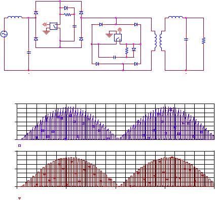
136 An Update on Power Quality
These spiky voltages across the switches may be excessively high, about thousand of kilovolt and which may destroy the switches during the operation of the circuit. Remedial measures should be taken to prevent this phenomenon to make the circuit commercially viable. In the proposed circuit RC snubbers are used for suppressing surge voltage across the switches. The power circuit of the proposed regulator with input output filter and snubbers is shown in Fig. 19.
Snubber enhances the performance of the switching circuits and results in higher reliability, higher efficiency, higher switching frequency, smaller size and lower EMI. The basic intent of a snubber is to absorb energy from the reactive elements in the circuit. The benefits of this may include circuit damping, controlling the rate of change of voltage or current or clamping voltage overshoot. The waveforms of voltages across switches with input output filters and snubbers are shown in Fig. 20.
Use of snubbers reduces the spiky voltage across the switches to a tolerate limit for practical application of the AC voltage regulator.
L1 |
L2 |
30mH |
SW1 |
S1 |
1R5 |
|
|
|
30mH |
|
+ |
+ |
|
|
|
|
|
||
|
|
|
|
|
|
|
||
Input |
- |
- |
C5 |
|
|
SW2 |
TX1 |
|
0 |
|
|
|
|
|
|||
|
|
0.1u |
- |
+ |
S2 |
|
|
|
VAMPL = 300 |
|
|
0 |
- |
+ |
|
C2 |
R3 |
FREQ = 50 |
|
|
|
|
|
|
5u |
100 |
|
|
|
|
|
R6 |
|||
|
|
|
|
|
|
|
||
C1 |
|
|
C3 |
0.1u |
|
1 |
|
|
5u |
|
|
|
|
|
|
|
|
|
|
|
|
|
|
|
0 |
|
0 |
Figure 19. The power circuit of the proposed AC voltage regulator with input output filters and
snubbers. |
|
|
|
|
400V |
|
|
|
|
200V |
|
|
|
|
0V |
V(S1:3)- V(S1:4) |
|
|
|
400V |
|
|
|
|
|
|
|
|
|
200V |
|
|
|
|
SEL>> |
|
|
|
|
0V |
5ms |
10ms |
15ms |
20ms |
0s |
||||
|
V(S2:3)- V(S2:4) |
Time |
|
|
|
|
|
|
Figure 20. Voltage across switches with filters and snubbers. V(S1:3)-V(S1:4): Voltage across switch-1, V(S2:3)-V(S2:4): Voltage across switch-2.
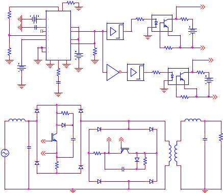
Power Quality Improvement Using Switch Mode Regulator 137
3.5. Proposed AC voltage regulator with practical switches
In the previous section, we have studied the regulator using ideal S-break switches which have been operated by the pulses from the limiter. But for practical application, real switches are essential which are to be controlled by the pulses having ground isolation. The proposed AC voltage regulator circuit with practical switches is shown in Fig. 21. The ideal S-break switch is replaced by IGBT.
In the proposed regulator chip SG1524B is used to control the gate signal. Signal from the chip is fed to the Limiter and finally to the optocoupler. The output of the optocoupler is used to control the on off time of the IGBTs. The function of the Limiter is to limit the output voltage of the gate signal generating IC from 0 to 6 volts. Optocoupler is used to generate signaling voltage with ground isolation.
|
|
|
|
|
U1 |
|
|
|
R1 |
|
|
|
|
|
|
|
|
|
|
|
|
|
|
|
16 3 |
|
|
|
|
|
|
|
|
|
|||
|
|
|
|
|
|
|
0 |
|
|
|
|
|
|
|
S2 |
|||
R3 |
|
20Vdc V1 |
|
|
|
|
|
VREF |
OSC |
|
|
|
R15 |
U3 |
|
R8 |
|
|
50k |
0 |
|
|
15 |
VIN |
|
|
|
|
|
A4N25A |
|
|
|||||
|
|
C1 |
12 |
|
6 |
|
|
|
|
V3 |
|
|||||||
|
0 |
|
|
7 |
CT |
|
|
C_A |
|
|
|
|
|
|
||||
|
4000pf |
6 |
|
|
11 |
|
2 |
|
|
|
|
15V |
|
|||||
|
|
RT |
|
|
E_A |
|
|
|
|
|
|
|||||||
|
|
|
|
1 |
|
|
|
|
0 |
|
|
|
|
|
|
|||
|
|
|
|
ERR- |
|
|
|
|
|
|
|
|
|
|||||
|
|
|
|
2 |
|
13 |
|
|
|
0 |
|
|
|
|||||
|
|
|
|
ERR+ |
C_B |
|
|
|
|
|
|
|
||||||
R4 |
|
|
|
|
14 |
|
|
|
|
R6 |
|
|
||||||
|
|
|
|
4 |
CL+ |
COMP |
E_B |
|
|
|
|
|
|
|
|
G2 |
||
|
|
|
|
SHUT |
V2 |
|
|
|
|
|
|
|
||||||
1 |
|
|
|
5 |
|
R5 |
|
|
|
|
|
|||||||
|
|
|
|
|
CL- |
|
10Vdc |
|
|
|
|
|
|
|
||||
|
|
|
|
|
GND |
|
|
|
|
|
|
|
|
|
||||
|
|
|
|
|
|
|
|
|
|
|
|
|
|
|
S1 |
|||
|
0 |
|
|
0 |
|
|
|
|
SG1524B |
0 |
|
U2A |
6 |
|
|
R9 |
||
|
V6 |
|
8 |
|
9 |
10 |
|
3 |
2 |
R16 |
U4 |
|
||||||
|
|
100uVdc |
|
0 |
|
R20 |
0 |
|
2 |
|
A4N25A |
V4 |
||||||
|
|
|
|
|
|
1k |
|
|
|
0 |
|
|
15V |
|||||
|
|
|
|
|
|
|
|
|
|
|
|
|
|
|
|
|||
|
|
|
|
|
|
|
|
|
C2 |
|
|
|
|
|
|
|
|
|
|
|
|
|
|
|
|
|
|
|
|
CD4009A |
|
|
|
|
|
|
|
|
|
0 |
|
|
|
|
|
|
0.001u |
|
|
|
|
|
R7 |
|
||
|
|
|
|
|
|
|
|
|
|
|
|
|
0 |
|
||||
|
|
|
|
|
|
|
|
|
0 |
|
|
|
|
|
|
|
G1 |
|
|
|
|
|
|
|
|
|
|
|
|
|
|
|
|
|
|
||
|
L1 |
|
|
D1 |
|
|
|
|
|
D3 |
|
|
|
|
|
L2 |
|
|
|
|
|
|
|
|
|
|
1 R10 |
|
|
|
|
|
|
|
|
||
|
|
|
|
|
|
|
|
|
|
|
|
|
|
|
|
|
|
|
|
30mH |
|
|
Z1 |
|
|
|
|
|
|
|
|
|
|
|
30mH |
|
|
|
|
|
|
|
|
|
|
D9 |
|
|
|
|
|
|
|
|
|
|
|
|
|
|
|
|
|
|
|
|
D5 |
|
S2 |
|
D6 |
|
|
100 |
|
|
|
|
|
S1 |
|
|
|
|
|
|
G2 |
|
TX1 |
|
||||
|
|
|
|
|
|
|
|
C6 |
|
|
|
C4 |
||||||
|
V5 |
C3 |
|
|
|
|
|
|
0.1u |
|
R11 |
|
Z2 |
|
|
5u |
R14 |
|
|
|
|
G1 |
|
|
|
|
|
|
|
|
|
|
|
||||
|
|
5u |
|
|
|
|
|
|
|
|
|
|
|
|
|
|
|
|
|
|
|
|
|
|
|
|
|
|
|
|
|
|
|
|
|
|
|
VAMPL = 300 |
|
D2 |
|
|
|
R12 |
|
0.001 |
C5 |
D10 |
R13 |
|
|
|
||||
FREQ = 50 |
|
|
|
|
|
D4 |
|
|
1 |
|
|
|
||||||
|
|
|
|
|
|
|
|
|
0.001 |
|
|
|
|
|
|
|
|
|
|
|
|
|
|
|
|
|
|
|
|
D7 |
0.1u |
D8 |
|
|
|
||
|
|
|
|
|
|
|
|
|
|
0 |
|
|
|
|
|
|
|
0 |
Figure 21. Manually controlled AC voltage regulator circuit with practical switches.
3.5.1. Chip SG1524B for generation of gate signal
The Block diagram of the internal circuitry of the chip SG1524B is shown in Fig. 22. By controlling the error signals of the error amplifier the duty cycle of the gate signal to the
138 An Update on Power Quality
regulator can be controlled. Thus it is a very suitable device for using in the regulator circuits.
3.5.2. Results of proposed AC voltage regulator (practical switch implementation)
The waveforms of the input and output voltages of the proposed regulator are shown in Fig. 23 and Fig. 24. Fig. 23 shows the input and output voltages waveform when the input voltage is 200V and output voltage is 300V. Fig. 24 shows the input and output voltages waveform when the input voltage is 400V and output voltage is 300V. Fig. 25 and Fig. 26 show the input and output current waveforms corresponding to Fig. 23 and Fig. 24.
VCC |
15 |
Reference |
|
16 REF OUT |
|
Regulator |
|
||||
|
|
|
Vref |
|
|
|
|
|
Vref |
12 COL 1 |
|
|
|
|
|
11 EMIT 1 |
|
|
|
|
T |
13 |
COL 2 |
|
|
|
Vref |
|
|
|
6 |
|
14 |
EMIT 2 |
|
RT |
|
Oscillator |
3 |
||
CT |
7 |
|
|
OSC OUT |
|
|
1 |
Vref |
Vref |
|
|
IN - |
|
|
|
||
– |
|
|
|
||
IN + |
2 |
+ |
Comparator |
|
|
COMP 9 |
Vref |
Error Amplifier |
|
|
|
CURR LIM + |
4 |
|
|
||
+ |
|
|
|
||
5 |
|
|
|
||
CURR LIM - |
|
– |
|
|
|
SHUTDOWN 10 |
1 kΩ |
|
|
|
|
GND 8 |
10 kΩ |
|
|
|
|
|
|
|
|
||
Figure 22. Block diagrm of IC chip SG1524B
400V
0V 
-400V
0s |
50ms |
100ms |
150ms |
200ms |
V1(V5) |
V(R14:2) |
Time |
|
|
|
|
|
|
Figure 23. Input and output voltage waveforms, Input 200V output 300V. V1(V5): Input voltage – dotted line, V(R14:2): Output voltage – solid line.
Power Quality Improvement Using Switch Mode Regulator 139
400V |
|
|
|
|
0V |
|
|
|
|
-400V |
50ms |
100ms |
150ms |
200ms |
0s |
||||
V1(V5) |
V(R14:2) |
Time |
|
|
|
|
|
|
Figure 24. Input and output voltage waveforms, Input 400V output 300V. V1(V5): Input voltage – dotted line, V(R14:2): Output voltage – solid line.
5.0A |
|
|
|
|
0A |
|
|
|
|
-5.0A |
50ms |
100ms |
150ms |
200ms |
0s |
||||
-I(V5) |
-I(R14) |
Time |
|
|
|
|
|
|
Figure 25. Input and output current waveforms for input 200V output 300V. -I(V5): Input current - dotted line, -I(R14): Output current – solid line.
4.0A |
|
|
|
|
0A |
|
|
|
|
-4.0A |
50ms |
100ms |
150ms |
200ms |
0s |
||||
-I(V5) |
-I(R14) |
Time |
|
|
|
|
|
|
Figure 26. Input and output current waveforms for input 400V output 300V. -I(V5): Input current – dotted line, -I(R14): Output current – solid line.

140 An Update on Power Quality
From the waveforms shown in Fig. 23 to Fig. 26, it is seen that the waveforms of output voltage and input current is perfectly sinusoidal. The variation of output voltage of the proposed regulator with the duty cycle is shown in Fig. 27. The value of input voltage is kept constant to 300V. From Fig. 23 it is seen that the variation of output voltage with duty cycle is almost linear. The variation of duty cycle with the variation of input voltage from 200V to 400V to maintain the output voltage constant to 300V is shown in Fig. 28.
(V) |
600 |
|
|
|
|
|
|
|
|
500 |
|
|
|
|
|
|
|
|
|
voltage |
|
|
|
|
|
|
|
|
|
400 |
|
|
|
|
|
|
|
|
|
300 |
|
|
|
|
|
|
|
|
|
Output |
|
|
|
|
|
|
|
|
|
200 |
|
|
|
|
|
|
|
|
|
100 |
|
|
|
|
|
|
|
|
|
|
|
|
|
|
|
|
|
|
|
|
0.2 |
0.3 |
0.4 |
0.5 |
0.6 |
0.7 |
0.8 |
0.9 |
1 |
Duty cycle
Figure 27. Variation of output voltage with duty cycle. Input voltage is 300V.
|
0.8 |
|
|
|
|
|
cycle |
0.7 |
|
|
|
|
|
0.6 |
|
|
|
|
|
|
0.5 |
|
|
|
|
|
|
Duty |
|
|
|
|
|
|
0.4 |
|
|
|
|
|
|
0.3 |
|
|
|
|
|
|
|
|
|
|
|
|
|
|
0.2 |
|
|
|
|
|
|
175 |
225 |
275 |
325 |
375 |
425 |
|
|
|
Input voltage (V) |
|
|
|
Figure 28. Variation of duty cycle with input voltage to maintain output voltage constant to 300V.
4. Automatic controlled AC voltage regulator
In manually controlled AC voltage regulator control, the output voltage is sensed with a voltmeter connected at the output; the decision and correcting operation is made by a human judgment. The manual control may not be feasible always due to various factors. In automatic voltage regulators, all functions are performed by instruction, and give much better performance, so far as stability, speed of correction, consistency, fatigue, etc. are concerned.
Power Quality Improvement Using Switch Mode Regulator 141
There are two types of automatic control voltage regulator, discontinuous control and continuous control. The automatic control system consists of a sensing or measuring unit and a power control or regulating unit. The sensing unit compares the output voltage or the controlled variable with a steady reference and gives an output proportional to their difference called the error signal. The error voltage is amplified, integrated or differentiated or modified whenever necessary. The processed error voltage is fed to the main control unit to have required corrective action.
In the discontinuous type of control, the measuring unit is such as to produce no signal as long as the voltage is within certain limits. When the voltage goes outside this limit, a signal is produced by the measuring unit until the voltage is again brought within this limit. In this type of measuring or sensing unit, the correcting voltage is independent of percentage of error. When the voltage is brought back to this limit, the signal from the measuring unit is zero and the regulating unit remains at its new position until another signal is received from the measuring unit.
In continuous control, the measuring unit produces a signal with amplitude proportional to the difference between the fixed reference and the controlled voltage. The output of the measuring unit is zero when the controlled voltage or a fraction of it is equal to the reference voltage. The regulating or the controlling unit, which is associated with the continuous measuring unit, gives a correcting voltage proportional to the output of the measuring unit. The principle of operation of a continuous control AC voltage regulator is described in this section.
4.1. Control and gate signal generating circuit for controlled AC voltage regulator
Figure 29 shows the circuit of the proposed automatic controlled AC voltage regulator including the control and gate signal generating circuit. A fraction of the output voltage after capacitor voltage dividing and rectifying is passed through an OPAMP buffer. Buffer is used to remove the loading effect. Output voltage of the buffer is same as its input voltage. The output voltage of the buffer is further reduces using resistive voltage divider and taken as the negative input of the error amplifier of the PWM voltage regulating IC SG1524B.
The positive input of the error amplifier is taken from the reference voltage of the chip, after voltage dividing using 50K and 1 ohm resistance. The positive input of the error amplifier is fixed and the negative input is error signal which will vary according to the output voltage. Since the error signal is applied to the negative input of the error amplifier, the duty cycle will be increased if the error signal is decreased and vice versa.
When the output voltage increases above the set value which is 300V either due to change in input voltage or load, the error signal will be increased, therefore the duty cycle will decrease. As a result less power will be transferred from the input to output, and output voltage start to decrease until it reaches to the set value.
When the output voltage decreases below the set value either due to change in input voltage or load then error signal will be decreased which will increase the duty cycle. As a result,
142 An Update on Power Quality
more power will be transferred from the input to output, and output voltage start to increase until it reaches to the set value.
When the output voltage is same as the set value than the negative and positive input of the error amplifier will be same as a result the duty cycle will remain same and output voltage will remain unchanged. In this way the proposed regulator will maintain output voltage constant, irrespective of the variation of input voltage and load.
50k 0
0
R14
R4
1
 0
0
L1
30mH
V5
FREQ = 50 VAMPL = 300
C3
5u
|
|
|
U1 |
|
16 3 |
|
|
|
|
|
|
|
|
|
S2 |
|
|
|||
|
20Vdc V1 |
|
|
|
|
R1 |
|
|
|
R15 |
U3 |
|
R8 |
|
|
|
||||
|
C1 |
VIN |
VREF |
OSC |
0 |
|
|
|
V3 |
|
||||||||||
|
|
|
15 |
|
|
|
|
|
|
|
|
|
|
A4N25A |
|
|
|
|
||
0 |
4000pf |
|
7 |
CT |
|
|
C_A |
|
12 |
|
6 |
|
|
|
|
|
|
|
|
|
|
|
|
|
|
2 |
|
|
|
|
|
15V |
|
||||||||
|
|
|
6 |
RT |
|
|
E_A |
|
11 |
|
|
|
|
|
|
|
||||
|
|
|
1 |
|
|
|
|
|
|
|
|
|
|
|
|
|
|
|||
|
|
|
ERR- |
|
|
|
|
0 |
|
|
|
|
|
|
|
|
||||
|
|
|
2 |
|
|
13 |
|
|
|
0 |
R6 |
|
|
|
|
|||||
|
|
|
ERR+ |
C_B |
|
|
|
|
|
|
|
|
|
|||||||
|
|
|
|
|
14 |
|
|
|
|
|
|
|
G2 |
|
||||||
|
|
|
4 |
CL+ |
COMP |
E_B |
|
|
|
|
|
|
|
|
|
|
|
|||
|
|
|
5 |
SHUT |
|
|
V2 |
R5 |
|
6 |
|
|
|
S1 |
|
|||||
|
|
|
|
GND |
|
|
|
|
10Vdc |
|
U2A |
|
|
|
|
|||||
|
|
|
|
CL- |
|
|
|
|
|
|
|
R16 |
U4 |
|
|
|
|
|||
|
|
|
0 |
8 |
|
9 |
10 |
|
|
|
0 3 |
2 |
2 |
|
A4N25A |
|
V4 |
|
||
|
|
|
|
|
0 |
|
R20 |
|
0 |
|
|
0 |
|
|
R9 |
|
15V |
|
||
|
|
SG1524B |
|
|
|
50k |
|
CD4009A |
|
|
|
|
|
|
|
|||||
|
|
|
|
|
|
|
|
|
|
|
|
|
|
|
||||||
|
|
|
|
|
C2 |
|
|
|
|
|
|
|
R7 |
|
|
|
||||
|
|
|
|
|
|
|
|
|
|
|
|
|
|
|
0 |
|
|
|
||
|
|
|
|
|
|
|
|
.001u |
|
|
|
|
|
|
|
|
|
G1 |
||
|
|
|
|
|
|
|
|
0 |
|
|
|
|
|
|
|
|
|
|
|
|
|
|
|
|
|
|
|
|
|
|
|
|
|
|
|
|
|
|
|
|
|
|
|
|
|
|
|
|
|
|
|
|
|
|
|
|
|
|
|
11 |
|
|
|
|
|
|
|
|
|
|
|
|
|
|
|
|
|
|
|
|
- |
|
2 |
|
|
|
|
|
|
|
|
|
|
|
|
|
|
|
|
|
|
0 |
- |
|
|
|
|
|
|
|
|
|
|
|
|
|
|
|
|
|
R18 |
|
V |
|
|
|
|
|
|
|
|
|
|
|
|
|
|
|
|
|
|
1 |
OUT LM324 |
|
||
|
|
|
|
|
|
|
|
|
|
|
|
|
|
|
|
|
|
|||
|
|
|
|
|
|
|
|
|
|
|
|
|
|
|
|
|
|
|
U5A |
|
R19 |
V+ |
+ |
3 |
|
|||
|
V7 |
|
|
|
|
|
|
|
4 |
|
|
|
R10 |
|
|
|
|
|
0 |
|
20V |
D1 |
D3 |
|
|
|
|
L2 |
0 |
|
|
|
|
|
|
|
|
||||
|
1 |
|
|
|
|
|
30mH |
|
|
|
|
|
|
|
|
|
|
0.1u |
|
|
D9 |
|
|
|
|
|
|
|
|
|
|
D5 |
|
|
|
D6 |
|
C7 |
|
S1 |
|
C6 |
G2 |
S2 |
|
|
|||
|
Z1 |
|
|
|
|
Z3 |
TX1 |
100 |
|
|
0.1u |
R11 |
|
|
|
||||
G1 |
|
|
|
C4 |
R3 |
|
|||
|
|
|
|
|
|
|
|||
|
|
|
|
|
|
|
|
||
|
|
|
0.001 |
|
|
5u |
|
|
|
|
|
|
|
|
R13 |
|
|
||
|
R12 |
D4 |
|
C5 |
D10 |
|
|
0.3u |
|
|
|
|
1 |
|
|||||
D2 |
0.001 |
|
|
|
|
|
|
10u |
R17 |
|
|
|
D7 |
0.1u |
|
D8 |
|
C9 |
|
|
|
|
|
C8 |
4000k |
||||
|
|
|
|
|
|
|
|
||
0 |
0 |
|
Figure 29. Automatic controlled AC voltage regulator circuit with practical switches.
4.2. Results of automatic controlled AC voltage regulator
Figure 30 shows the input and output voltage waveforms of the proposed automatic controlled AC voltage regulator when the input voltage is 250V and output voltage is 300V. Figure 31 shows the input and output voltage waveforms of the proposed regulator when the input voltage is 350V and output voltage is 300V. Figure 32 and Fig. 33 shows the
Power Quality Improvement Using Switch Mode Regulator 143
waveforms of the input current and output currents corresponding to the waveforms of Fig. 30 and Fig. 31 for a load of 100 Ω.
400V
0V 


-400V
V(R14:2)
400V
0V 


SEL>> -400V
0s 100ms 200ms 300ms 400ms 500ms 600ms
 V1(V5)
Time
Figure 30. Input and output voltage waveforms for input 250V and output 300V. V1(V5): Input voltagebottom figure, V(R14:2): Output voltage – top figure.
500V
0V 
SEL>> -500V
V(R14:2)
400V
0V
-400V
0s 100ms 200ms 300ms 400ms 500ms 600ms
 V1(V5)
Time
Figure 31. Input and output voltage waveforms for input 350V and output 300V. V1(V5): Input voltagebottom figure, V(R14:2): Output voltage – top figure.
Table 1 summarizes the result of the proposed regulator to regulate output voltage to 300V for variation of input voltage from 200V to 350V and load from 100 ohm to 200 ohm. In this

144 An Update on Power Quality
table input current, output current, input power factor, and efficiency of the regulator are also provided. The proposed regulator can regulate the output voltage effectively, for a wide variation of input voltage and load with efficiency of more than 90% and input power factor more than 0.9.
4.0A
0A 


SEL>> -4.0A
 -I(R14)
5.0A
0A 

-5.0A
0s 100ms 200ms 300ms 400ms 500ms 600ms
-I(V5)
Time
Figure 32. Input and output current waveforms for input 250V output 300V. -I(V5): Input current – bottom figure, -I(R14): Output current – top figure.
5.0A |
|
|
|
|
|
0A |
|
|
|
|
|
SEL>> |
|
|
|
|
|
-5.0A |
-I(R14) |
|
|
|
|
|
|
|
|
|
|
5.0A |
|
|
|
|
|
0A |
|
|
|
|
|
-5.0A |
|
|
|
|
|
0s |
100ms |
200ms |
300ms |
400ms |
500ms 600ms |
|
-I(V5) |
|
Time |
|
|
|
|
|
|
|
Figure 33. Input and output current waveforms for input 350V output 300V. -I(V5): Input current – bottom figure, -I(R14): Output current – top figure.
Power Quality Improvement Using Switch Mode Regulator 145
Vin |
I in |
Input pf |
Pin |
Vout (V) |
Load |
Iout |
Pout |
Efficiency |
(V) |
(A) |
|
(W) |
|
(Ω) |
(A) |
(W) |
(%) |
200 |
4.81 |
1.00 |
481 |
295 |
100 |
2.95 |
435.13 |
90.46 |
225 |
4.30 |
1.00 |
483.09 |
298 |
100 |
2.98 |
444.02 |
91.91 |
250 |
3.92 |
1.00 |
489.70 |
300 |
100 |
3.00 |
450.00 |
91.89 |
275 |
3.60 |
1.00 |
495.00 |
300 |
100 |
3.00 |
450.00 |
90.91 |
300 |
3.30 |
1.00 |
493.79 |
300 |
100 |
3.00 |
450.00 |
91.13 |
325 |
3.10 |
0.99 |
498.85 |
302 |
100 |
3.02 |
456.02 |
91.41 |
350 |
2.95 |
0.98 |
508.41 |
305 |
100 |
3.05 |
465.13 |
91.49 |
250 |
2.07 |
0.96 |
248.73 |
300 |
200 |
1.50 |
225.00 |
90.46 |
275 |
1.90 |
0.95 |
248.46 |
300 |
200 |
1.50 |
225.00 |
90.56 |
300 |
1.75 |
0.95 |
248.20 |
300 |
200 |
1.50 |
225.00 |
90.65 |
325 |
1.68 |
0.93 |
253.12 |
302 |
200 |
1.51 |
228.01 |
90.08 |
350 |
1.60 |
0.91 |
253.77 |
305 |
200 |
1.53 |
232.56 |
91.64 |
*All voltages and currents values in this table are in peak values.
Table 1. Results of proposed automatic controlled AC voltage regulator for maintaining output 300 V.
5. Conclusion
An essential feature of efficient electronic power processing is the use of semiconductors devices in switch mode to control the transfer of energy from source to load through the use of pulse width modulation techniques. Inductive and capacitive energy storage elements are used to smooth the flow of energy while keeping losses at a lower level. As the frequency of the switching increases, the size of the capacitive and inductive elements decreases in a direct proportion. Because of the superior performance, the SMPS are replacing conventional linear power supplies.
In this chapter the design and analysis of an AC voltage regulator operated in switch mode is described in details. AC voltage regulator is used to maintain output voltage constant either for an input voltage variation or load variation to improve the power quality. If the output voltage remains constant, equipment life time increases and outages and maintenance are reduced.
At first the regulator is analyzed using ideal switches, then the ideal switches is replaced by practical switches which required isolated gate signal. The procedure of smoothing the input current and output voltage, and suppressing the surge voltage across the switches is described. A manually controlled AC voltage regulator is analyzed then the concept of operation of an automatic controlled AC voltage regulator is described. Finally an automatic controlled AC voltage regulator is designed and its performance is analyzed.
The proposed regulator can maintain the output voltage constant to 300V, when input voltage is vary from 200V to 350V also for variation of load. To maintain constant output voltage PWM control is used. By varying the duty cycle of the control circuit have achieved the goal of maintaining the constant output voltage across load. For generation of gate
146 An Update on Power Quality
signal of the switches an IC chip SG1524B is used which is compact and commercially available at a very low cost. The input current of the proposed regulator is sinusoidal and the input power factor is above 0.9. From simulation results it is seen that the efficiency of the proposed regulator is more than 90%.
Author details
Raju Ahmed
Electrical and Electronic Engineering Department, Dhaka University of Engineering and Technology (DUET), Gazipur, Bangladesh
Mohammad Jahangir Alam
Electrical and Electronic Engineering Department, Bangladesh University of Engineering and Technology (BUET), Dhaka, Bangladesh
6. References
[1]P. B. Steciuk and J. R. Redmon, “Voltage sag analysis peaks customer service,” IEEE Comput. Appl. Power, vol. 9, pp. 48-51, Oct. 1996.
[2]M. F. McGranaghan, D. R. Mueller, and M. J. Samotyj, “Voltage sags in industrial systems,” IEEE Transactions on Industrial Application., vol. 29, pp. 397-403, Mar./Apr. 1993.
[3]M. H. J. Bollen, “The influence of motor reacceleration on voltage sags,” IEEE Transactions on Industrial Application, vol. 31, pp. 667-674, July/Aug. 1995.
[4]M. H. J. Bollen, “Characterization of voltage sags experienced by three phase adjustable-speed drives,” IEEE Transactions on Power Delivery, vol. 12, pp. 1666-1671, Oct. 1997.
[5]H. G. Sarmiento and E. Estrada, “A voltage sag study in an industry with adjustable speed drives”,IEEE Industry Applications Magazine., vol. 2, pp. 16-19, Jan./Feb. 1996.
[6]N. Kutkut, R. Schneider, T. Grand, and D. Divan, “AC voltage regulation technologies,” Power Quality Assurance, pp. 92-97, July/Aug. 1997.
[7]D. Divan, P. Sulherland, and T. Grant, “Dynamic sag corrector: A new concept in power conditioning,” Power Quality Assurance, pp.42-48, Sept./Oct. 1998.
[8]A. Elnadt and Magdy M. A. Salama, “Unified approach for mitigating voltage sag and voltage flicker using the DSTATCOM,” IEEE Transactions on Power Delivery, vol. 30, no. 2, April 2005.
[9]S. M. Hietpas and R. Pecan, “Simulation of a three-phase boost converter to compensate for voltage sags, ” in Proceeding. IEEE 1998 Rural Electric Power Conference, pp. B4-1- B4-7, Apr. 1998.
[10]S. M. Hietpas and Mark Naden, “Automatic voltage regulator using an AC voltagevoltage converter,” IEEE Transactions on Industrial Application, vol. 36, pp. 33-38, Jan.\Feb. 2000.
[11]F. Z. Peng, Lihue Chen, and Fan Zhang, “Simple topologies of PWM AC-AC converters,” IEEE Power Electronics Letters, vol. 1, no.1, March 2003.
Power Quality Improvement Using Switch Mode Regulator 147
[12]G. Venkataramanan. B. K. Johnson, and A. Sundaram, “An AC-AC power converter for custom power applications,” IEEE Transactions on Power Delivery, vol. 11, pp. 16661671, July 1996.
[13]V. Nazquez, A. Velazquez, C. Hernandez, E. Rodríguez and R. Orosco, “A Fast AC Voltage Regulator,”, CIEP 2008. 11th IEEE International Power Electronics Congress, pp. 162-166, Aug. 2008.
[14]J. Nan, T. Hou-jun, L. Wei and Y. Peng-sheng, “Analysis and control of Buck-Boost Chopper type AC voltage regulator,”, IPEC’09. IEEE 6th International Power Electronics and Motion Control Conference, pp. 1019-1023, May 2009.
[15]N. A. Ahmed, M. Miyatake, H. W. Lee and M. Nakaoka, “A Novel Circuit Topology of Three-Phase Direct AC-AC PWM Voltage Regulator” Industry Applications Conference, 2006. 41st IAS Annual Meeting. Conference Record of the 2006 IEEE, pp. 2076-2081, Oct. 2006.
[16]V. Nazquez, A. Velazquez and C. Hernandez, “AC Voltage Regulator Based on the ACAC Buck-Boost Converter,” ISIE 2007. IEEE International Symposium on Industrial Electronics, pp. 533-537, Jun. 2007.
[17]P. K. Banerjee, “Power line voltage regulation by PWM AC Buck-Boost voltage controller,” A M.Sc. thesis, Department of EEE, BUET, July, 2002.
[18]A. Hossain, “AC voltage regulation by Cûk switch mode power supply,” A M.Sc. thesis, Department of EEE, BUET, July, 2003.
[19]Li B. H., Choi S.S., Vilathgamuwa D. M., Design considerations on the line-side filter used in the dynamic voltage restorer, IEE Proceedings - Generation, Transmission, and Distribution, pp. 1-7, 2001.
[20]Wang Jing, Xu Aiqin, Shen Yueyue., A Survey on Control Strategies of Dynamic Voltage Restorer, 13th International Conference on Harmonics and Quality of Power (ICHQP), pp. 1-5, Sept. 28 2008-Oct. 1, 2008,.
[21]Nielsen J.G., Blaabjerg F., A Detailed Comparison of System Topologies for Dynamic Voltage Restorers, IEEE Transactions on Industry Applications, vol, 41, no. 5, pp. 12721280, 2005.
[22]OrCAD Software, Release 9: 1985-1999 OrCAD, Inc., U.S.A.
[23]Slobodan Cûk, "Basics of Switched Mode Power Conversion Topologies, Magnetics, and Control,” Modern Power Electronics: Evaluation, Technology, and applications, Edited by B.K. Bose, IEEE Press, pp. 265-296, 1992.
[24]M. H. Rashid," Power Electronics – Circuits, Devices, and Applications, "Prenctice Hall India, Second Edition, 2000, pp.317-387.
[25]P.C. Sen, "Power Electronics,” Tata McGraw-Hill Publishing Company Ltd., India, 1987, pp. 588-614.
[26]R. Thompson, "A Thyristor Alternating Voltage Regulator,” IEEE Trans. on Ind. and Gen. Application, vol. IGA 4 (1968) 2, pp. 162-166., 1968.
[27]E. J. Cham and W. R. Roberts, “Current Regulators for Large Rectifier Power Supplies Used on Electrochemical Processing Lines,” IEEE Trans. on Ind. and Gen. Application IGA-4 (1968) 6, pp. 609-618.
[28]J. M.(Jr), Mealing , "A Coherent Approach to the Design of Switching Mode DC Regulators,” IEEE Conf. Rec. IGA, pp.177-185, Oct. 1967.
148An Update on Power Quality
[29]Unitrode, "Switching Regulated Power Supply Design Seminar Manual,” Unitrode Corporation, U. S. A, 1986.
[30]M. H. Rashid, "A Thyristor Chopper With Minimum Limits on Voltage Control of DC Drives, " International Jurnal of Electronics, Vol. 53, No. 1, pp.71-81, 1982.
[31]K. P. Severns and G. E. Bloom, “Modern DC-to-DC Switch Mode Power Converter Circuits,” Van Nostrand Reinholdd Company, Inc., New York, U. S. A, 1983.
[32]S. Cûk, "Survey of Switched Mode Power Supplies,” IEEE International Conference on Power Electronics and Variable Speed Drives, London, pp. 83-94, 1985.
[33]M. Ehsani, R. L. Kustom, and R. E. Fuja, "Microprocessor Control of A Current Source DC-DC Converter,” IEEE Transactions on Industrial Applications, Vol. LA19, No. 5, pp. 690-698, 1983.
[34]R. D. Middlebrook, “A Continuous Model for the Tapped-Inductor Boost Converter," IEEE Power Electronics Specialists Conference Record, Culver City, CA, U. S. A, pp.6379, 1975.
[35]Slobodan Cûk R. D. Middlebrook, "A General Unified Approach to Modeling Switching DC-to-DC Converters in Discontinuous Conduction Mode," IEEE Power Electronics Specialists Conference Record, Palo Alto, CA, U. S. A, pp. 36-57, 1977.
[36]R. D. Middlebrook and Slobodan Cûk, "Modeling and Analysis Methods for DC-to-DC Switching Converters,” IEEE International Semiconductor Power Converter Conference Record, Lake Buena Vista, FL, U. S. A, pp.90-111, 1977.
[37]Slobodan Cûk and R. D. Middlebrook, “Coupled Inductor and other Extensions of a New Optimum Topology Switching DC-to-DC Converter,” IEEE Industry Applications Society Annual Meeting, Record, Los Angeles, CA, U. S. A, pp.1110-1126, 1977.
[38]R. D. Middlebrook and Slobodan Cûk, “Isolation and Multiple Output Extensions of a New Optimum Topology Switching DC-to-DC Converter,” IEEE Power Electronics Specialists Conference Record, Syracuse, NY, U. S. A, pp.256-264, 1978.
[39]C. Chen and Deepakraj M. Divan, “Simple Topologies for Single Phase AC Line Conditioning,” IEEE Transactions on Industry Applications, Vol.30, No.2, pp. 406-412, March/April 1994.
[40]Mark F. McGranaghan, David R. Mueller and Marek J. Samotyj, “Voltage Sags in Industrial Systems,” IEEE Transactions on Industry Applications, Vol.29, No.2, pp. 397403, March/April 1993.
[41]S. Cûk and R. D. Middlebrook, "Advances in Switched Mode Power Conversion," IEEE Transactions on Industrial Electronics, Vol. IE 30. No. 1, pp.10-29, 1983.
[42]N. Mohan, Tore M. Undeland and William P.Robbins, “Power ElectronicsConverters, Applications, and Design, " John Wiley and Sons Inc., Second ed., pp. 161-195 & 669695, 1995
[43]H. Veffer, “High Current, Low Inductance GTO and IGBT Snubber Capacitors,” Siemens Components, June, pp. 81-85, 1990.
[44]B. D. Bedford and R. G. Hoft, "Principles of Inverter Circuits,” Wiley: 1964.
[45]E. R. Hnatek, “Design of Solid-State Power Supplies,” Van Nostrand Reinhold; 1971.
[46]A. I. Pressman, “Switching and Linear Power Supply,” Power Converter Design, vol. I and vol. II, Hayden; 1977.