

plc analog - 22.9
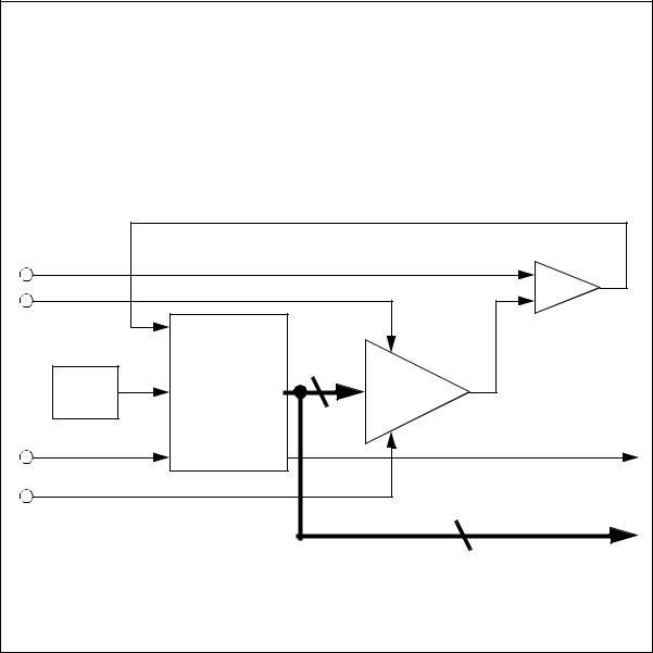
ASIDE: This device is an 8 bit A/D converter. The main concept behind this is the successive approximation logic. Once the reset is toggled the converter will start by setting the most significant bit of the 8 bit number. This will be converted to a voltage Ve that is a function of the +/-Vref values. The value of Ve is compared to Vin and a simple logic check determines which is larger. If the value of Ve is larger the bit is turned off. The logic then repeats similar steps from the most to least significant bits. Once the last bit has been set on/off and checked the conversion will be complete, and a done bit can be set to indicate a valid conversion value.
Vin above (+ve) or below (-ve) Ve
Vin |
+ |
- |
+Vref |
|
successive |
8 |
|
|
clock |
approximation |
D to A |
|
|
converter |
|
|||
logic |
Ve |
|||
|
||||
|
|
|||
reset |
|
|
done |
|
-Vref |
|
|
8 |
|
|
|
data out |
||
|
|
|
Quite often an A/D converter will multiplex between various inputs. As it switches the voltage will be sampled by a sample and hold circuit. This will then be converted to a digital value. The sample and hold circuits can be used before the multiplexer to collect data values at the same instant in time.
Figure 22.7 A Successive Approximation A/D Converter
22.2.1 Analog Inputs With a PLC
The PLC 5 ladder logic in Figure 22.8 will control an analog input card. The Block Transfer Write (BTW) statement will send configuration data from integer memory to the analog card in rack 0, slot 0. The data from N7:30 to N7:66 describes the configuration for different input channels. Once the analog input card receives this it will start doing analog

plc analog - 22.10
conversions. The instruction is edge triggered, so it is run with the first scan, but the input is turned off while it is active, BT10:0/EN. This instruction will require multiple scans before all of the data has been written to the card. The update input is only needed if the configuration for the input changes, but this would be unusual. The Block Transfer Read (BTR) will retrieve data from the card and store it in memory N7:10 to N7:29. This data will contain the analog input values. The function is edge triggered, so the enable bits prevent it from trying to read data before the card is configured BT10:0/EN. The BT10:1/EN bit will prevent if from starting another read until the previous one is complete. Without these the instructions experience continuous errors. The MOV instruction will move the data value from one analog input to another memory location when the BTR instruction is done.
|
update |
BT10:0/EN |
BTW |
|
|
||||||
|
|
|
|||||||||
|
|
|
|
|
Rack: 0 |
|
|
||||
|
|
|
|
|
|
|
|
|
|
|
|
|
|
|
|
|
|
|
|
|
Group: 0 |
|
|
|
|
|
|
|
|
|
|
|
|
|
|
|
|
|
|
|
|
|
|
|
Module: 0 |
|
|
|
|
|
|
|
|
|
|
|
BT Array: BT10:0 |
|
|
|
|
|
|
|
|
|
|
|
Data File: N7:30 |
|
|
|
|
|
|
|
|
|
|
|
|
|
|
|
|
|
|
|
|
|
|
|
Length: 37 |
|
|
|
S2:1/15 |
|
|
|
|
|
|
||||
|
|
|
|
|
Continuous: no |
|
|
||||
|
|
|
|
|
|
|
|
|
|
|
|
|
|
|
|
|
|
|
|
|
|||
|
|
|
|
|
|
|
|
|
|
|
|
|
BT10:0/EN BT10:1/EN |
BTR |
|
|
|||||||
|
|
|
|
|
|
|
|
|
Rack: 0 |
|
|
|
|
|
|
|
|
|
|
|
|
|
|
|
|
|
|
|
|
|
|
|
Group: 0 |
|
|
|
|
|
|
|
|
|
|
|
Module: 0 |
|
|
|
|
|
|
|
|
|
|
|
BT Array: BT10:1 |
|
|
|
|
|
|
|
|
|
|
|
Data File: N7:10 |
|
|
|
|
|
|
|
|
|
|
|
Length: 20 |
|
|
|
|
|
|
|
|
|
|
|
Continuous: no |
|
|
|
BT10:1/DN |
|
|
|
|
|
|
|
|||
|
|
|
|
|
|
note: |
|||||
|
|
|
|
|
MOV |
||||||
|
|
|
|
|
|
|
|
|
|||
|
|
|
|
|
|
|
|
|
Source N7:15 |
analog |
|
|
|
|
|
|
|
|
|
|
|||
|
|
|
|
|
|
|
|
|
Dest N7:0 |
channel #2 |
|
|
|
|
|
|
|
|
|
|
|||
|
|
|
|
|
|
|
|
|
|
|
|
Note: The basic operation is that the BTW will send the control block to the input card. The inputs are used because the BTR and BTW commands may take longer than one scan.
Figure 22.8 Ladder Logic to Control an Analog Input Card
The data to configure a 1771-IFE Analog Input Card is shown in Figure 22.9.
plc analog - 22.11
(Note: each type of card will be different, and you need to refer to the manuals for this information.) The 1771-IFE is a 12 bit card, so the range will have up to 2**12 = 4096 values. The card can have 8 double ended inputs, or 16 single ended inputs (these are set with jumpers on the board). To configure the card a total of 37 data words are needed. The voltage range of different inputs are set using the bits in word 0 (N7:30) and 1 (N7:31). For example, to set the voltage range on channel 10 to -5V to 5V we would need to set the bits, N7:31/3 = 1 and N7:31/2 = 0. Bits in data word 2 (N7:32) are set to determine the general configuration of the card. For example, if word 2 was 0001 0100 0000 0000b the card would be set for; a delay of 00010 between samples, to return 2s compliment results, using single ended inputs, and no filtering. The remaining data words, from 3 to 36, allow data values to be scaled to a new range. Words 3 and 4 are for channel 1, words 5 and 6 are for channels 2 and so on. To scale the data, the new minimum value is put in the first word (word 3 for channel 1), and the maximum value is put in the second word (word 4 for channel 1). The card then automatically converts the actual data reading between 0 and 4095 to the new data range indicated in word 3 and 4. One oddity of this card is that the data values for scaling must always be BCD, regardless of the data type setting. The manual for this card claims that putting zeros in the scaling values will cause the card to leave the data unscaled, but in practice it is better to enter values of 0 for the minimum and 4095 for the maximum.

plc analog - 22.12
N7:30 |
0 |
R8 |
R8 |
R7 |
R7 |
R6 |
R6 |
R5 |
R5 |
|
R4 |
R4 |
R3 |
R3 |
R2 |
R2 |
R1 |
R1 |
||
|
|
|||||||||||||||||||
|
1 |
R16 |
R16 |
R15 |
R15 |
R14 |
R14 |
R13 |
R13 |
|
R12 |
R12 |
R11 |
R11 |
R10 |
R10 |
R9 |
R9 |
||
|
2 |
S |
S |
S |
S |
S |
N |
N |
T |
|
F |
F |
F |
F |
F |
F |
F |
F |
||
|
3 |
|
|
|
|
|
|
|
L1 |
|
|
|
|
|
|
|
|
|||
|
4 |
|
|
|
|
|
|
|
U1 |
|
|
|
|
|
|
|
|
|||
|
5 |
|
|
|
|
|
|
|
L2 |
|
|
|
|
|
|
|
|
|||
|
6 |
|
|
|
|
|
|
|
U2 |
|
|
|
|
|
|
|
|
|||
|
|
|
|
|
|
|
|
|
|
|
|
|
|
|
|
|
|
|
|
|
|
|
|
|
|
|
|
|
|
|
|
|
|
|
|
|
|
|
|
|
|
|
|
|
|
|
|
|
|
|
|
|
|
|
|
|
|
|
|
|
|
|
|
|
|
|
|
|
|
|
|
|
|
|
|
|
|
|
|
|
|
|
|
|
|
|
|
|
|
|
|
|
|
|
|
|
|
|
|
|
|
|
|
|
|
|
|
|
|
|
|
|
|
|
|
|
|
|
|
|
|
|
|
|
|
33 |
|
|
L15 |
34 |
|
|
U15 |
35 |
|
|
L16 |
36 |
|
|
U16 |
R1,R2,...R16 - range values |
00 |
1 to 5V |
|
|
|
01 |
0 to 5V |
|
|
10 |
-5 to 5V |
|
|
11 |
-10 to 10V |
T - input type - (0) gives single ended, (1) gives double ended
N - data format - |
00 |
BCD |
|
||
|
01 |
not used |
|
10 |
2’s complement binary |
|
11 |
signed magnitude binary |
F - filter function - a value of (0) will result in no filtering, up to a value of (99BCD)
S - real time sampling mode - (0) samples always, (11111binary) gives long delays.
L1,L2,...L16 - lower input scaling word values
U1,U2,...,U16 - upper input scaling word values
Figure 22.9 Configuration Data for an 1771-IFE Analog Input Card
The block of data returned by the BTR statement is shown in Figure 22.10. Bits 0- 2 in word 0 (N7:10) will indicate the status of the card, such as error conditions. Words 1 to 4 will reflect status values for each channel. Words 1 and 2 indicate if the input voltage is outside the set range (e.g., -5V to 5V). Word 3 gives the sign of the data, which is