

Ceramic Technology and Processing, King
.pdfCeramic Property Measurements 453
Another common use of a SEM is to look at fracture surfaces in order to identify the fracture origin. Figure 11.46 depicts the fracture surface of a TZP ceramic with a rather evident fracture origin.
Figure 11.46: Microstructural Flaw in a Yttria-Stabilized Zirconia FineGrained, Dense Ceramic. Fracture surface. SEM Photograph. The arrow points to what appears to be an agglomerate. Scale bar 10 μm.
The arrow points to the flaw that appears to be an agglomerate. If it were a different material, it would probably display cracks around the edges as the firing shrinkage would likely be different. With the analytical capability of EDX, the composition of the flaw can be determined, with the intent of removing this material from the powder so that it won't happen again. Observing fracture origins is common, as the ceramic selectively chooses to break there.

454 Ceramic Technology and Processing
What else can be learned from looking at SEM photos of ceramics? Take, for example, the surface shown in Figure 11.47.
Figure 11.47: Wear Surface on an Alumina/Zirconia Abrasive Grain. SEM photograph. The stainless steel phase was molten during machining. Scale bar 10 μm.
Ceramic materials are used as abrasives; this one is an alumina- zirconia-fused grain used for machining stainless steel. It is obvious from the photo that the temperature was above 1429 °C, which is the melting point of 304 stainless steel.
It is written that polishing is a process of finer and finer abrasion. This is not always true, as seen in Figure 11.48.

Ceramic Property Measurements 455
Figure 11.48: Wear Surface on a B4C Colloid Mill Plate. SEM photograph. The wear surface is grooved and polished. The arrow points to a groove with residual alumina. Scale bar 200 μm.
This is the wear surface of a B4C wear plate in a colloid mill used for comminuting an alumina powder. Some of the alumina is seen stuck in the wear grooves on the surface. Note two things. First, boron carbide is much harder than alumina and cannot be abraded by it. Second, the wear surface is polished, implying that wear is by a molecular-scale process where abrasion is by a relatively macro-scale process. Polished wear surfaces are usually the result of diffusion and chemical processes, rather than mechanical. Thinking of wear as centrally related to mass transport reduces confusion. There are exactly four mass transport processes:
•diffusion,
•viscous flow,

456Ceramic Technology and Processing
•fracture and kinetic displacement, and
•plastic deformation.
Examination of wear surfaces often indicates which of these four, alone or in combination, is the wear mechanism. This often leads to conclusions as to what can be done to lower the wear rate. In the case of the B4C wear surface, the process was likely chemical, involving diffusion and viscous flow. A change of material is indicated.
The next example of the power of the SEM is concerned with the heavy-duty machining of steel.3 Steel has a structure where the carboncontaining phase is clustered as Fe3C ceramic domains, seen in Figure 11.49.
Figure 11.49: Microstructure of Steel. SEM photograph of a polished section. The arrow points to the Fe3C pearlite ceramic phase. The matrix is iron. Scale bar 10 μm.

Ceramic Property Measurements 457
There are two phases present, alpha iron and pearlite (Fe3C). Iron is a malleable metal. Pearlite is a brittle, hard ceramic. When the surface is severely deformed, the pearlite clusters mash down into layers as seen in Figure 11.50.
Figure 11.50: Layers of Flattened Pearlite due to Shear caused by Rough Machining. SEM photograph of a polished section. Arrow points to a flattened pearlite phase. Scale bar 10 μm.
The shear surface is at the top of the picture and, in that region, the layers of pearlite are flattened. Using the SEM at higher magnification on this region near the surface, one can observe a high concentration of Fe3C platlets to the point that the surface is nearly all pearlite, as seen in Figure 11.51. (Incidentally, carbon was detected in this phase with EDX.)

458 Ceramic Technology and Processing
Figure 11.51: Concentration of the Pearlite Ceramic on the Wear Surface as shown by the arrow. SEM photograph of a polished section. The wear surface is almost all pearlite. Scale bar 10 μm.
From these observations, one can deduce the mechanism. Start with an analogy. Take a thin sheet of plywood (pearlite) and cover it with an inch of Jello (alpha iron). Build that order up for several layers. Now, jump on the stack. Obviously, the Jello will squirt out on the sides leaving just the plywood on the surface. That also occurs when machining the steel. This understanding is made possible from contemplation of the SEM.
As mentioned earlier, an SEM can be equipped with analytical capability, either energy-dispersive or wavelength-dispersive techniques. Using these techniques, the chemical composition of the surface can be determined. As with all analytical methods, there are some limitations, but these are not especially restrictive and the analytical tools are generally very useful. The combination of a wide range of magnification, great depth of

Ceramic Property Measurements 459
field, and analytical capability makes the SEM one of the best problem solvers around.
Energy Dispersive Analysis. In this method, the secondary fluorescent X- rays are separated into a spectrum by their energy. High frequencies have more energy than low frequencies and are spread out into a spectrum of peaks of varying magnitude. The instrument is smart and will label each peak as to what element it represents. As there is some overlap, the instrument will present a few choices, most of which are improbable, as they are rare in ceramic formulations. Elements from B (atomic number 5) on up, with a few exceptions, can be analyzed. Figure 11.52 shows an EDX attachment for either an SEM or TEM.
Figure 11.52: Energy Dispersive X-ray (EDX) Attachment for an Electron Microscope. Measures chemical composition of a surface. Very useful technique. Virtually mandatory. (Courtesy Oxford)

460 Ceramic Technology and Processing
The figure is of the sensor coupled to electronics not shown here. At low atomic numbers, sensitivity is low as the X-rays are soft (i.e., weak and easily absorbed). The same problems exist with energy-dispersive analysis as with bulk X-ray fluorescent analysis, since they are similar methods. The main problem is absorption by the matrix, which is more acute when the matrix contains elements that are strongly absorbing. Matrices with light elements are less troublesome. A set of related standards makes the method quantitative, with perhaps two significant figures.
Another useful ability of a SEM is the selectivity of the area to be analyzed. This can range from a 1 μm spot to a broad field. While the electron beam is about 1 μm in diameter or less, the radiation spills over and penetrates into the sample, limiting the smallest field to a few cubic micrometers. An additional attribute of this method is the selectivity it provides for the analysis. For example, the surface can be mapped for a single element, showing its distribution and rough concentration.
We will now discuss a ceramic problem where extensive wear of alumina abrasives occurs when machining titanium. Three figures are used to illustrate the example. Figure 11.53 shows a groove cut in titanium by an alumina cutter.
Figure 11.53: Groove Cut in Titanium with an Alumina Abrasive Point, SEM Photograph. The groove is striated. Scale bar 100 μm.

Ceramic Property Measurements 461
As can be seen, the groove is striated and smooth along the direction of the cut. Figure 11.54 is of the same field, except that the image was made from just the Al spectral lines.
Figure 11.54: Aluminum Concentration in the Same Groove (as in previous figure). SEM photograph with EDX Al Spectra. Aluminum has been transferred to the titanium metal. Scale bar 100 μm.
Aluminum (Al) is being transferred from the abrasive tip to the titanium (Ti) surface, without any visual evidence of particulates. The transfer is not by reduction of Al2O3 by Ti as the thermodynamics does not allow this to occur. If direct diffusion of Al into the titanium is not occuring, then something else is. Consider that Al and Ti are not the only phases present. There is also O2 present in the system, which is responsible for the
462 Ceramic Technology and Processing
material transfer in that Ti is oxidized at the high surface temperature and an aluminum titanate compound is then formed as an interstitial film. A traverse can be made across the groove using only the aluminum spectra, as seen in Figure 11.55.
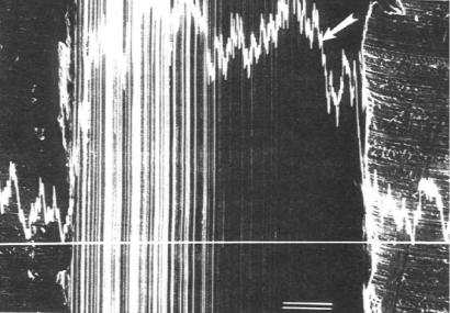
Figure 11.55: EDX Traverse across the Same Wear Groove, SEM photograph. Scan shows the distribution of aluminum. Arrow points to maximum Al. Scale bar 100 μm.
In the line scan, the concentration of Al is proportional to the height above the base line. When the curvature of the groove is considered, the Al distribution is fairly flat across the traverse. Line scans by the SEM and EDX are useful tools for studying surfaces, in particular when reactions are occurring. Wear of the alumina abrasive, in this case, was by diffusion, after oxidation of the Ti surface.