

- •Table of Contents
- •INTRODUCTION TO THE DSP56002
- •DSP56002 PIN DESCRIPTIONS
- •PORT A
- •PORT B
- •PORT C
- •PROGRAMMING SHEETS
- •List of Figures
- •List of Tables
- •1.1 INTRODUCTION
- •Figure 1-1 DSP56002 Technical Literature
- •1.2 FEATURES
- •Zero Overhead Nested DO Loops
- •512 x 24 Program RAM
- •Two 256 x 24 Data RAM
- •Two 256 x 24 Data ROM (Sine and Cosine Tables)
- •Synchronous Serial Interface Port
- •24 General Purpose I/O Pins
- •24-bit Timer/Event Counter
- •1.3 DSP56K CENTRAL PROCESSING UNIT OVERVIEW
- •Data Buses
- •Address Buses
- •Data Arithmetic Logic Unit (data ALU)
- •Address Generation Unit (AGU)
- •Program Control Unit (PCU)
- •Memory Expansion (Port A)
- •Figure 1-2 DSP56002 Block Diagram
- •1.4 MANUAL ORGANIZATION
- •INTRODUCTION TO THE DSP56002
- •2.1 INTRODUCTION
- •2.2 SIGNAL DESCRIPTIONS
- •Figure 2-1 DSP56002 Signals
- •2.2.1 Port A Address and Data Bus
- •2.2.2 Port A Bus Control
- •Table 2-1 Program and Data Memory Select Encoding
- •2.2.3 Interrupt and Mode Control
- •2.2.4 Power and Clock
- •2.2.5 Host Interface
- •2.2.6 Serial Communication Interface (SCI)
- •2.2.7 Synchronous Serial Interface (SSI)
- •2.3 ON-CHIP EMULATION (OnCE) PINS
- •2.3.1 Debug Serial Input/Chip Status 0 (DSI/OS0)
- •2.3.2 Debug Serial Clock/Chip Status 1 (DSCK/OS1)
- •2.3.3 Debug Serial Output (DSO)
- •2.3.4 Debug Request Input (DR)
- •2.4 PLL PINS
- •2.5 TIMER/EVENT COUNTER MODULE PIN
- •SECTION 2
- •DSP56002 PIN DESCRIPTIONS
- •3.1 MEMORY MODULES AND OPERATING MODES
- •3.2 DSP56002 DATA AND PROGRAM MEMORY
- •3.2.1 Program Memory
- •3.2.2 X Data Memory
- •3.2.3 Y Data Memory
- •Figure 3-1 DSP56002 Memory Maps
- •3.3 DSP56002 OPERATING MODE REGISTER (OMR)
- •3.3.1 Chip Operating Mode (Bits 0 and 1)
- •Figure 3-2 OMR Format
- •3.3.2 Data ROM Enable (Bit 2)
- •3.3.3 Internal Y Memory Disable Bit (Bit 3)
- •Table 3-1 Memory Mode Bits
- •3.3.4 Chip Operating Mode (Bit 4)
- •3.3.5 Reserved (Bit 5)
- •3.3.6 Stop Delay (Bit 6)
- •3.4 DSP56002 OPERATING MODES
- •Table 3-2 DSP56002 Operating Mode Summary
- •3.4.1 Single Chip Mode (Mode 0)
- •3.4.2 Bootstrap From EPROM (Mode 1)
- •Figure 3-3 Port A Bootstrap Circuit
- •Table 3-3 Organization of EPROM Data Contents
- •3.4.3 Normal Expanded Mode (Mode 2)
- •3.4.4 Development Mode (Mode 3)
- •3.4.5 Reserved (Mode 4)
- •3.4.6 Bootstrap From Host (Mode 5)
- •3.4.7 Bootstrap From SCI (Mode 6)
- •3.4.8 Reserved (Mode 7)
- •3.5 DSP56002 INTERRUPT PRIORITY REGISTER
- •Table 3-4 Interrupt Vectors
- •Table 3-5 Exception Priorities Within an IPL
- •SECTION 3
- •4.1 INTRODUCTION
- •4.2 PORT A INTERFACE
- •Figure 4-1 Port A Signals
- •Figure 4-2 External Program Space
- •Figure 4-3 External X and Y Data Space
- •Figure 4-4 Memory Segmentation
- •Table 4-1 Program and Data Memory Select Encoding
- •4.3 PORT A TIMING
- •Figure 4-8 Mixed-Speed Expanded System
- •4.4 PORT A WAIT STATES
- •Table 4-2 Wait State Control
- •4.5 BUS CONTROL REGISTER (BCR)
- •Figure 4-9 Bus Control Register
- •Figure 4-10 Bus Strobe/Wait Sequence
- •4.6 BUS STROBE AND WAIT PINS
- •4.7 BUS ARBITRATION AND SHARED MEMORY
- •Figure 4-11 Bus Request/Bus Grant Sequence
- •Table 4-3 BR and BG During WAIT
- •1. DSP# 2 sets OUT1=0 (BR#1=0).
- •4.7.4 Signaling Using Semaphores
- •Figure 4-17 Signaling Using Semaphores
- •5.1 INTRODUCTION
- •Figure 5-1 Port B Interface
- •5.2 GENERAL PURPOSE I/O CONFIGURATION
- •Figure 5-2 Parallel Port B Registers
- •Figure 5-3 Parallel Port B Pinout
- •Figure 5-4 Port B I/O Pin Control Logic
- •5.2.1 Programming General Purpose I/O
- •Figure 5-5 On-Chip Peripheral Memory Map
- •5.2.2 Port B General Purpose I/O Timing
- •Figure 5-7 I/O Port B Configuration
- •5.3 HOST INTERFACE (HI)
- •Figure 5-8 HI Block Diagram
- •5.3.1 Host Interface – DSP CPU Viewpoint
- •5.3.2 Programming Model – DSP CPU Viewpoint
- •5.3.2.1 Host Control Register (HCR)
- •5.3.2.1.4 HCR Host Flag 2 (HF2) Bit 3
- •5.3.2.1.5 HCR Host Flag 3 (HF3) Bit 4
- •5.3.2.1.6 HCR Reserved Control (Bits 5, 6, and 7)
- •5.3.2.2 Host Status Register (HSR)
- •5.3.2.2.1 HSR Host Receive Data Full (HRDF) Bit 0
- •5.3.2.2.3 HSR Host Command Pending (HCP) Bit 2
- •5.3.2.2.4 HSR Host Flag 0 (HF0) Bit 3
- •5.3.2.2.5 HSR Host Flag 1 (HF1) Bit 4
- •Figure 5-10 Host Flag Operation
- •5.3.2.2.6 HSR Reserved Status (Bits 5 and 6)
- •5.3.2.2.7 HSR DMA Status (DMA) Bit 7
- •5.3.2.3 Host Receive Data Register (HRX)
- •5.3.2.4 Host Transmit Data Register (HTX)
- •5.3.2.5 Register Contents After Reset
- •5.3.2.6 Host Interface DSP CPU Interrupts
- •Figure 5-11 HSR–HCR Operation
- •5.3.2.7 Host Port Usage Considerations – DSP Side
- •5.3.3 Host Interface – Host Processor Viewpoint
- •Figure 5-13 HI Register Map
- •5.3.3.2 Interrupt Control Register (ICR)
- •5.3.3.2.1 ICR Receive Request Enable (RREQ) Bit 0
- •5.3.3.2.3 ICR Reserved Bit (Bit 2)
- •Table 5-2 HREQ Pin Definition
- •5.3.3.2.4 ICR Host Flag 0 (HF0) Bit 3
- •5.3.3.2.5 ICR Host Flag 1 (HF1) Bit 4
- •Table 5-3 Host Mode Bit Definition
- •5.3.3.2.7 ICR Initialize Bit (INIT) Bit 7
- •Table 5-4 HREQ Pin Definition
- •5.3.3.3 Command Vector Register (CVR)
- •Figure 5-14 Command Vector Register
- •5.3.3.3.2 CVR Reserved Bit (Bit 6)
- •5.3.3.3.3 CVR Host Command Bit (HC) Bit 7
- •5.3.3.4 Interrupt Status Register (ISR)
- •5.3.3.4.3 ISR Transmitter Ready (TRDY) Bit 2
- •5.3.3.4.4 ISR Host Flag 2 (HF2) Bit 3
- •5.3.3.4.5 ISR Host Flag 3 (HF3) Bit 4
- •5.3.3.4.6 ISR Reserved Bit (Bit 5)
- •5.3.3.4.7 ISR DMA Status (DMA) Bit 6
- •5.3.3.4.8 ISR Host Request (HREQ) Bit 7
- •5.3.3.5 Interrupt Vector Register (IVR)
- •5.3.3.6 Receive Byte Registers (RXH, RXM, RXL)
- •5.3.3.7 Transmit Byte Registers (TXH, TXM, TXL)
- •5.3.3.8 Registers After Reset
- •Table 5-5 Host Registers after Reset (Host Side)
- •5.3.4 Host Interface Pins
- •5.3.4.3 Host Read/Write (HR/W)
- •5.3.4.4 Host Enable (HEN)
- •5.3.4.5 Host Request (HREQ)
- •Table 5-6 Port B Pin Definitions
- •5.3.4.6 Host Acknowledge (HACK)
- •5.3.5 Servicing the Host Interface
- •Figure 5-15 Host Processor Transfer Timing
- •1. Polling
- •2. Interrupts, which can be either
- •5.3.5.1 HI Host Processor Data Transfer
- •5.3.5.2 HI Interrupts Host Request (HREQ)
- •Figure 5-16 Interrupt Vector Register Read Timing
- •5.3.5.3 Polling
- •Figure 5-17 HI Interrupt Structure
- •Figure 5-18 DMA Transfer Logic and Timing
- •5.3.5.5 Servicing DMA Interrupts
- •5.3.6 HI Application Examples
- •5.3.6.1 HI Initialization
- •Figure 5-19 HI Initialization Flowchart
- •Figure 5-20 HI Initialization–DSP Side
- •Figure 5-21 (a) HI Configuration–Host Side
- •Figure 5-22 Host Mode and INIT Bits
- •2. Assert HACK If the interface is using HACK
- •5. Assert HEN to enable the HI
- •5.3.6.2.1 Host to DSP - Data Transfer
- •Figure 5-23 Bits Used for Host-to-DSP Transfer
- •Figure 5-24 Data Transfer from Host to DSP
- •5. Writing data to TXL clears TXDE in the ISR.
- •5.3.6.2.2 Host to DSP – Command Vector
- •Figure 5-27 HI Exception Vector Locations
- •Figure 5-28 Host Command
- •2. The HC is then set.
- •3. The HCP bit in the HSR is set when HC is set.
- •Figure 5-25 Receive Data from Host–Main Program
- •Figure 5-29 Bootstrap Using the HI
- •Figure 5-30 Transmit/Receive Byte Registers
- •Figure 5-31 Bootstrap Code Fragment
- •5.3.6.2.4 DSP to Host Data Transfer
- •Figure 5-32 Bits Used for DSP to Host Transfer
- •Figure 5-33 Data Transfer from DSP to Host
- •5.3.6.3 DMA Data Transfer
- •Figure 5-36 HI Hardware–DMA Mode
- •5.3.6.3.1 Host To DSP Internal Processing
- •1. HI asserts the HREQ pin when TXDE=1.
- •Figure 5-37 DMA Transfer and Host Interrupts
- •3. When HACK is asserted, the HI deasserts HREQ.
- •Figure 5-39 Host-to-DSP DMA Procedure
- •Figure 5-38 Host Bits with TREQ and RREQ
- •5.3.6.3.2 Host to DSP DMA Procedure
- •5.3.6.3.3 DSP to Host Internal Processing
- •5.3.6.3.4 DSP to Host DMA Procedure
- •Figure 5-40 DSP to Host DMA Procedure
- •5.3.6.4 Example Circuits
- •Figure 5-41 MC68HC11 to DSP56002 Host Interface
- •Figure 5-42 MC68000 to DSP56002 Host Interface
- •Figure 5-43 Multi-DSP Network Example
- •2. Overwriting Transmit Byte Registers:
- •4. Overwriting the Host Vector:
- •5. Cancelling a Pending Host Command Exception:
- •6.1 INTRODUCTION
- •Figure 6-1 Port C Interface
- •6.2 GENERAL-PURPOSE I/O (PORT C)
- •Figure 6-2 Port C GPIO Control
- •Figure 6-3 Port C GPIO Registers
- •Figure 6-4 Port C I/O Pin Control Logic
- •6.2.1 Programming General Purpose I/O
- •Figure 6-6 Write/Read Parallel Data with Port C
- •Figure 6-7 I/O Port C Configuration
- •6.2.2 Port C General Purpose I/O Timing
- •6.3 SERIAL COMMUNICATION INTERFACE (SCI)
- •6.3.1 SCI I/O Pins
- •6.3.1.1 Receive Data (RXD)
- •6.3.1.2 Transmit Data (TXD)
- •6.3.1.3 SCI Serial Clock (SCLK)
- •6.3.2 SCI Programming Model
- •Figure 6-9 SCI Programming Model
- •6.3.2.1 SCI Control Register (SCR)
- •Figure 6-10 Serial Formats (Sheet 1 of 2)
- •Table 6-1 Word Formats
- •6.3.2.1.2 SCR SCI Shift Direction (SSFTD) Bit 3
- •6.3.2.1.3 SCR Send Break (SBK) Bit 4
- •6.3.2.1.4 SCR Wakeup Mode Select (WAKE) Bit 5
- •6.3.2.1.5 SCR Receiver Wakeup Enable (RWU) Bit 6
- •6.3.2.1.7 SCR Receiver Enable (RE) Bit 8
- •6.3.2.1.8 SCR Transmitter Enable (TE) Bit 9
- •6.3.2.1.14 SCR SCI Clock Polarity (SCKP) Bit 15
- •6.3.2.2 SCI Status Register (SSR)
- •6.3.2.2.1 SSR Transmitter Empty (TRNE) Bit 0
- •6.3.2.2.4 SSR Idle Line Flag (IDLE) Bit 3
- •6.3.2.2.5 SSR Overrun Error Flag (OR) Bit 4
- •6.3.2.2.6 SSR Parity Error (PE) Bit 5
- •6.3.2.2.7 SSR Framing Error Flag (FE) Bit 6
- •6.3.2.2.8 SSR Received Bit 8 Address (R8) Bit 7
- •6.3.2.3 SCI Clock Control Register (SCCR)
- •Figure 6-11 16 x Serial Clock
- •6.3.2.3.2 SCCR Clock Out Divider (COD) Bit 12
- •6.3.2.3.3 SCCR SCI Clock Prescaler (SCP) Bit 13
- •Figure 6-12 SCI Baud Rate Generator
- •6.3.2.4 SCI Data Registers
- •6.3.2.4.1 SCI Receive Registers
- •Figure 6-13 Data Packing and Unpacking
- •6.3.2.4.2 SCI Transmit Registers
- •6.3.3 Register Contents After Reset
- •6.3.4 SCI Initialization
- •Figure 6-14 SCI Initialization Procedure
- •6.3.5 SCI Exceptions
- •Figure 6-16 SCI Exception Vector Locations
- •6.3.6 Synchronous Data
- •Figure 6-18 Synchronous Slave
- •Figure 6-19 Synchronous Timing
- •Figure 6-20 SCI Synchronous Transmit
- •Figure 6-21 SCI Synchronous Receive
- •6.3.7 Asynchronous Data
- •6.3.7.1 Asynchronous Data Reception
- •6.3.7.2 Asynchronous Data Transmission
- •Figure 6-27 Transmitting Marks and Spaces
- •6.3.8 Multidrop
- •6.3.8.1 Transmitting Data and Address Characters
- •6.3.8.3 Idle Line Wakeup
- •Figure 6-32 Idle Line Wakeup
- •6.3.8.4 Address Mode Wakeup
- •6.3.8.5 Multidrop Example
- •6.3.9 SCI Timer
- •Figure 6-35 SCI Timer Operation
- •Figure 6-36 SCI Timer Example (Sheet 1 of 2)
- •Figure 6-37 DSP56002 Bootstrap Example - Mode 6
- •Figure 6-38 Bootstrap Code Fragment
- •6.3.11 Example Circuits
- •Figure 6-39 Synchronous Mode Example
- •Figure 6-41 Multimaster System Example
- •Figure 6-40 Master-Slave System Example
- •6.4 SYNCHRONOUS SERIAL INTERFACE (SSI)
- •6.4.1 SSI Data and Control Pins
- •6.4.1.1 Serial Transmit Data Pin (STD)
- •6.4.1.2 Serial Receive Data Pin (SRD)
- •6.4.1.3 Serial Clock (SCK)
- •6.4.1.4 Serial Control Pin (SC0)
- •Table 6-7 SSI Operation: Flag 0 and Rx Clock
- •6.4.1.5 Serial Control Pin (SC1)
- •Table 6-8 SSI Operation: Flag 1 and Rx Frame Sync
- •6.4.1.6 Serial Control Pin (SC2)
- •Table 6-9 SSI Operation: Tx and Rx Frame Sync
- •6.4.2 SSI Programming Model
- •Figure 6-45 SSI Programming Model (Sheet 1 of 2)
- •6.4.2.1 SSI Control Register A (CRA)
- •Table 6-10 Number of Bits/Word
- •6.4.2.1.4 CRA Prescaler Range (PSR) Bit 15
- •6.4.2.2 SSI Control Register B (CRB)
- •6.4.2.2.1 CRB Serial Output Flag 0 (OF0) Bit 0
- •6.4.2.2.2 CRB Serial Output Flag 1 (OF1) Bit 1
- •Figure 6-46 Serial Control, Direction Bits
- •6.4.2.2.6 CRB Clock Source Direction (SCKD) Bit 5
- •6.4.2.2.7 CRB Shift Direction (SHFD) Bit 6
- •Table 6-11 Frame Sync Length
- •6.4.2.2.9 CRB Sync/Async (SYN) Bit 9
- •6.4.2.2.10 CRB Gated Clock Control (GCK) Bit 10
- •6.4.2.2.11 CRB SSI Mode Select (MOD) Bit 11
- •6.4.2.2.12 CRB SSI Transmit Enable (TE) Bit 12
- •6.4.2.2.13 CRB SSI Receive Enable (RE) Bit 13
- •6.4.2.3 SSI Status Register (SSISR)
- •6.4.2.3.1 SSISR Serial Input Flag 0 (IF0) Bit 0
- •6.4.2.3.2 SSISR Serial Input Flag 1 (IF1) Bit 1
- •6.4.2.3.9 SSI Receive Shift Register
- •Figure 6-47 Receive Data Path
- •6.4.2.3.10 SSI Receive Data Register (RX)
- •6.4.2.3.11 SSI Transmit Shift Register
- •Figure 6-48 Transmit Data Path
- •6.4.2.3.12 SSI Transmit Data Register (TX)
- •6.4.2.3.13 Time Slot Register (TSR)
- •6.4.3 Operational Modes and Pin Definitions
- •6.4.4 Registers After Reset
- •Table 6-14 SSI Registers After Reset
- •6.4.5 SSI Initialization
- •Figure 6-49 SSI Initialization Block Diagram
- •Figure 6-50 SSI CRA Initialization Procedure
- •Figure 6-51 SSI CRB Initialization Procedure
- •Figure 6-52 SSI Initialization Procedure
- •6.4.6 SSI Exceptions
- •Figure 6-53 SSI Exception Vector Locations
- •Figure 6-54 SSI Exceptions
- •Table 6-17 SSI Operating Modes
- •6.4.7.1 Data/Operation Formats
- •6.4.7.1.1 Normal/Network Mode Selection
- •6.4.7.1.2 Continuous/Gated Clock Selection
- •Figure 6-58 CRB GCK Bit Operation
- •Figure 6-62 Synchronous Communication
- •Figure 6-63 CRB SYN Bit Operation
- •Figure 6-64 Gated Clock — Synchronous Operation
- •6.4.7.1.4 Frame Sync Selection
- •Figure 6-68 CRB FSL0 and FSL1 Bit Operation
- •6.4.7.1.5 Shift Direction Selection
- •Figure 6-71 CRB SHFD Bit Operation (Sheet 1 of 2)
- •6.4.7.2 Normal Mode Examples
- •6.4.7.2.1 Normal Mode Transmit
- •Figure 6-72 Normal Mode Example
- •2. SC2 is TX and RX frame sync out
- •3. STD is transmit data out
- •4. SCK clocks the transmit data out
- •6.4.7.2.2 Normal Mode Receive
- •6.4.7.3 Network Mode Examples
- •Figure 6-75 Network Mode Example
- •Figure 6-76 TDM Network Software Flowchart
- •Figure 6-77 Network Mode Initialization
- •6.4.7.3.1 Network Mode Transmit
- •6.4.7.3.2 Network Mode Receive
- •Figure 6-80 On Demand Example
- •Figure 6-81 On-Demand Data-Driven Network Mode
- •Figure 6-82 Clock Modes
- •Figure 6-83 SPI Configuration
- •6.4.8 Flags
- •Figure 6-88 Output Flag Example
- •Figure 6-89 Output Flag Initialization
- •Figure 6-90 Input Flags
- •6.4.9 Example Circuits
- •Figure 6-91 SSI Cascaded Multi-DSP System
- •Figure 6-92 SSI TDM Parallel DSP Network
- •Figure 6-96 SSI TDM Bus DSP Network
- •SECTION 6
- •PORT C
- •7.1 INTRODUCTION
- •7.2 TIMER/EVENT COUNTER BLOCK DIAGRAM
- •Figure 7-2 Timer/Event Counter Programming Model
- •7.3 TIMER COUNT REGISTER (TCR)
- •7.4 TIMER CONTROL/STATUS REGISTER (TCSR)
- •7.4.1 Timer Enable (TE) Bit 0
- •7.4.2 Timer Interrupt Enable (TIE) Bit 1
- •7.4.3 Inverter (INV) Bit 2
- •Table 7-1 Timer/Event Counter Control Bits
- •GPIO*
- •Internal
- •Timer (Mode 0)
- •Output
- •Internal
- •Timer Pulse (Mode 1)
- •Output
- •Internal
- •Timer Toggle (Mode 2)
- •Reserved - Do Not Use
- •Input
- •Internal
- •Input Width (Mode 4)
- •Input
- •Internal
- •Input Period (Mode 5)
- •Input
- •External
- •Standard Time Counter (Mode 6)
- •Input
- •External
- •Event Counter (Mode 7)
- •7.4.5 General Purpose I/O (GPIO) Bit 6
- •7.4.6 Timer Status (TS) Bit 7
- •7.4.7 Direction (DIR) Bit 8
- •7.4.8 Data Input (DI) Bit 9
- •7.4.9 Data Output (DO) Bit 10
- •7.4.10 TCSR Reserved bits (Bits 11-23)
- •7.5 TIMER/EVENT COUNTER MODES OF OPERATION
- •Figure 7-3 Standard Timer Mode (Mode 0)
- •Figure 7-4 Timer/Event Counter Disable
- •7.5.4 Timer Mode 4 (Pulse Width Measurement Mode)
- •Figure 7-8 Pulse Width Measurement Mode (INV=0)
- •Figure 7-9 Pulse Width Measurement Mode (INV=1)
- •7.5.5 Timer Mode 5 (Period Measurement Mode)
- •Figure 7-10 Period Measurement Mode (INV=0)
- •Figure 7-11 Period Measurement Mode (INV=1)
- •7.7 OPERATING CONSIDERATIONS
- •7.8 SOFTWARE EXAMPLES
- •7.8.1 General Purpose I/O Input
- •7.8.2 General Purpose I/O Output
- •7.8.4 Pulse Width Measurement Mode (Timer Mode 4)
- •7.8.5 Period Measurement Mode (Timer Mode 5)
- •A.1 INTRODUCTION
- •Table B-2 Instruction Set Summary — Sheet 1 of 5
- •Figure B-2 Status Register (SR)
- •Figure B-3 Bus Control Register (BCR)
- •Figure B-7 Port B Control Register (PBC)
- •Figure B-8 Port B Data Direction Register (PBDDR)
- •Figure B-9 Port B Data Register (PBD)
- •Figure B-10 Port C Control Register (PCC)
- •Figure B-12 Port C Data Register (PCD)
- •Figure B-17 Host Transmit Data Register (HTX)
- •Figure B-13 Port B Control Register (PBC)
- •Figure B-14 Host Control Register (HCR)
- •Figure B-16 Host Receive Data Register (HRX)
- •Figure B-15 Host Status Register (HSR)
- •Figure B-19 Command Vector Register (CVR)
- •Figure B-18 Interrupt Control Register (ICR)
- •Figure B-20 Interrupt Status Register (ISR)
- •Figure B-21 Interrupt Vector Register (IVR)
- •Figure B-24 Port C Control Register (PCC)
- •Figure B-25 SCI Control Register (SCR)
- •Figure B-27 SCI Clock Control Register (SCCR)
- •Figure B-29 SCI Receive Data Registers
- •Figure B-28 SCI Transmit Data Registers
- •Figure B-30 SSI Control Register (PCC)
- •Figure B-31 SSI Control Register A (CRA)
- •Figure B-32 SSI Control Register B (CRB)
- •Figure B-33 SSI Status Register (SSISR)
- •Figure B-35 Timer Count Register (TCR)
- •INDEX

Freescale Semiconductor, Inc.
Freescale Semiconductor, Inc.
SERIAL COMMUNICATION INTERFACE (SCI)
routine for minimum overhead. This interrupt is enabled by SCR bit 11 (RIE).
2.SCI Receive Data with Exception Status – caused by receive data register full with a receiver error (parity, framing, or overrun error). The SCI status register must be read to clear the receiver error flag. A long interrupt service routine should be used to handle the error condition. This interrupt is enabled by SCR bit 11 (RIE).
3.SCI Transmit Data – caused by transmit data register empty. This error-free interrupt may use a fast interrupt service routine for minimum overhead. This interrupt is enabled by SCR bit 12 (TIE).
4.SCI Idle Line – occurs when the receive line enters the idle state (10 or 11 bits of ones). This interrupt is latched and then automatically reset when the interrupt is accepted. This interrupt is enabled by SCR bit 10 (ILIE).
5.SCI Timer – caused by the baud rate counter underflowing. This interrupt is automatically reset when the interrupt is accepted. This interrupt is enabled by SCR bit 13 (TMIE).
6.3.6Synchronous Data
The synchronous mode (WDS=0, shift register mode) is designed to implement seri- al-to-parallel and parallel-to-serial conversions. This mode will directly interface to 8051/8096 synchronous (mode 0) buses as both a controller (master) or a peripheral (slave) and is compatible with the SSI mode if SCKP equals one. In synchronous mode, the clock is always common to the transmit and receive shift registers.
As a controller (synchronous master) shown in Figure 6-17, the DSP puts out a clock on the SCLK pin when data is present in the transmit shift register (a gated clock mode). The master mode is selected by choosing internal transmit and receive clocks (setting TCM and RCM=0). The example shows a 74HC165 parallel-to-serial shift register and 74HC164 serial-to-parallel shift register being used to convert eight bits of serial I/O to eight bits of parallel I/O. The load pulse latches eight bits into the 74HC165 and then
SCLK shifts the RXD data into the SCI (these data bits are sample bits 0-7 in the timing diagram). At the same time, TXD shifts data out (B0-B7) to the 74HC164. When using the internal clock, data is transmitted when the transmit shift register is full. Data is valid on both edges of the output clock, which is compatible with an 8051 microprocessor. Received data is sampled in the middle of the clock low time if SCKP equals zero or in the middle of the clock high time if SCKP equals one. There is a window during which STX must be written with the next byte to be transmitted to prevent a gap between words. This
MOTOROLA PORT C 6 - 39
For More Information On This Product, Go to: www.freescale.com

Freescale Semiconductor, Inc.
Freescale Semiconductor, Inc.
SERIAL COMMUNICATION INTERFACE (SCI)
6789 5 4 3 2 1 0 |
SCICONTROLREGISTER(SCR) |
(READ/WRITE) |
6789 5 4 3 2 1 0 |
SCICLOCKCONTROLREGISTER(SCCR) |
(READ/WRITE) |
|
B4B3B2 B5 B6 B7 |
|
XXXXXXXX XX XX XXXXXXX |
432 5 6 7 |
|
74HC165 D 8 PARALLEL INPUTS |
LQ LOAD PULSE |
|
|
|
Synchronous17-6Figure Master |
WAKERWUWOMSRETE SBK 0 0 0 0 |
SSFTD WDS2 WDS1 WDS0 |
CD5CD6CD7CD8CD9 CD4 CD3 CD2 CD1 CD0 |
|
|
STXWRITE |
I/OREGISTER |
CLK |
D |
74HC164 S/P |
||||||||
|
|
|
|
|
|
|
|
|
|
|
|
|
|
|
OUTPUTSPARALLEL8 |
|
|
|
|
|
|
|
|
|
|
|
|
|
|
|
|
|
Q |
|
|
|
|
|
|
|
|
|
|
|
|
|
|
|
|
|
CLK |
|
|
11 10 |
RIE ILIE |
|
11 10 |
CD11 CD10 |
|
|
B0 B1 |
|
XX |
0 1 |
EXAMPLE: SHIFT |
DSP56002 |
RXD |
SCLK |
TXD |
|
|
15 14 13 12 |
SCKP STIR TMIE TIE |
|
15 14 13 12 |
0 0 SCP COD |
TCM RCM |
CLOCK OUTPUT (SCP = 0) |
TRANSMIT DATA (SSFTD = 0) |
|
RECEIVE DATA XXXXXX |
SAMPLE |
|
|
|
|
|
|
|
|
X:$FFF0 |
|
X:$FFF2 |
|
|
|
|
|
|
|
|
|
|
|
|
||
6 - 40 PORT C MOTOROLA
For More Information On This Product, Go to: www.freescale.com
Freescale Semiconductor, Inc.
Freescale Semiconductor, Inc.
SERIAL COMMUNICATION INTERFACE (SCI)
window is from the time TDRE goes high halfway into transmission of bit 1 until the middle of bit 6 (see Figure 6-19(a)).
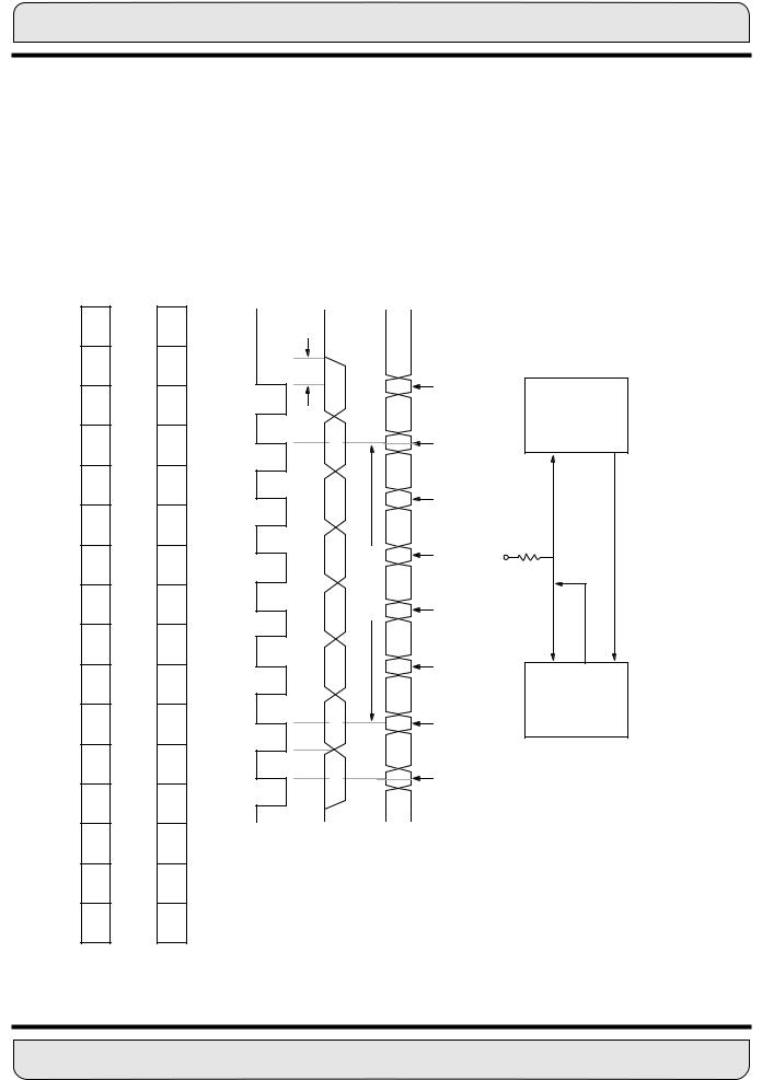
As a peripheral (synchronous slave) shown in Figure 6-18, the DSP accepts an input clock from the SCLK pin. If SCKP equals zero, data is clocked in on the rising edge of SCLK, and data is clocked out on the falling edge of SCLK. If SCKP equals one, data is clocked in on the falling edge of SCLK, and data is clocked out on the rising edge of SCLK. The slave mode is selected by choosing external transmit and receive clocks (TCM and RCM=1). Since there is no frame signal, if a clock is missed due to noise or any other reason, the receiver will lose synchronization with the data without any error signal being generated. Detecting an error of this type can be done with an error detecting protocol or with external circuitry such as a watchdog timer. The simplest way to recover synchronization is to reset the SCI.
The timing diagram in Figure 6-18 shows transmit data in the normal driven mode. Bit B7
is essentially one-half SCI clock long (TSCI/2 + 1.5 TEXTAL) The last data bit is truncated so that the pin is guaranteed to go to its reset state before the start of the next data word,
thereby delimiting data words. The 1.5 crystal clock cycles provide sufficient hold time to satisfy most external logic requirements. The example diagram requires that the WOMS bit be set in the SCR to wired-OR RXD and TXD, which causes TXD to be three-stated when not transmitting. Collisions (two devices transmitting simultaneously) must be avoided with this circuit by using a protocol such as alternating transmit and receive periods. In the example, the 8051 is the master device because it controls the clock. There is a window during which STX must be written with the next byte to be transmitted to prevent the current word from being retransmitted. This window is from the time TDRE goes high, which is halfway into the transmission of bit 1, until the middle of bit 6 (see Figure 6-19(b)). Of course, this assumes the clock remains continuous – i.e., there is a second word. If the clock stops, the SCI stops.
The DSP is initially configured according to the protocol to either receive data or transmit data.
If the protocol determines that the next data transfer will be a DSP transmit, the DSP will configure the SCI for transmit and load STX (or STXA). When the master starts SCLK, data will be ready and waiting. If the protocol determines that the next data transfer will be a DSP receive, the DSP will configure the SCI for receive and will either poll the SCI or enable interrupts. This methodology allows multiple slave processors to use the same data line. Selection of individual slave processors can be under protocol control or by multiplexing SCLK.
Note: TCM=0, RCM=1 and TCM=1,RCM=0 are not allowed in the synchronous mode.
The results are undefined.
The assembly program shown in Figure 6-20 uses the SCI synchronous mode to transmit only the low byte of the Y data ROM contents. The program sets the reset vector to run the program after a hardware reset, puts the MOVEP instruction at the SCI transmit inter-
MOTOROLA PORT C 6 - 41
For More Information On This Product, Go to: www.freescale.com
Freescale Semiconductor, Inc.
Freescale Semiconductor, Inc.
SERIAL COMMUNICATION INTERFACE (SCI)
|
SCICONTROLREGISTER(SCR) |
(READ/WRITE) |
|
SCICLOCKCONTROLREGISTER(SCCR) |
(READ/WRITE) |
cyc |
|
|
|
|
|
|
|
|
|
|
|
2 1 0 |
0 0 0 |
WDS2 WDS1 WDS0 |
2 1 0 |
CD2 CD1 CD0 |
|
1.5 t |
B7 |
|
|
XX XXXXXXX |
7 |
|
|
8051 |
OR |
8096 |
|
101112131415 9 8 7 6 5 4 3 |
ILIERIETIETMIESTIRSCKPTE RE WOMS RWU WAKE SBK 0 |
SSFTD |
101112131415 9 8 7 6 5 4 3 |
CD10CD11CODSCP11 CD9 CD8 CD7 CD6 CD5 CD4 CD3 |
RCMTCM |
INPUTCLOCK 0)=(SKP |
B6 |
0)=(SSFTD |
|
XXXXXXXXDATARECEIVEXX XX XX XX XX |
10SAMPLE 2 3 4 5 6 |
SYNCHRONOUSTOINTERFACEEXAMPLE: MICROCOMPUTER BUSES |
|
P3.0 |
|
P3.1 |
Figure 6-18 Synchronous Slave |
DATATRANSMIT |
WRITE STX |
DSP56002 |
RXD |
TXD |
SCLK |
||||||||||||
|
|
|
|
|
|
|
B5 |
|
|
|
|
|
|
|
|
|
|
|
|
|
|
|
|
|
B4 |
|
|
|
|
|
|
|
|
|
|
|
|
|
|
|
|
|
B3 |
|
|
|
|
|
|
|
|
|
|
|
|
|
|
|
|
|
B2 |
|
|
|
|
|
|
|
|
|
|
|
|
|
|
|
|
|
B1 |
|
|
|
|
|
|
|
|
|
|
|
|
|
|
|
|
|
B0 |
|
|
|
|
|
|
|
|
|
|
|
X:$FFF0 |
|
X:$FFF2 |
|
|
|
|
|
|
|
|
|
|
|
|
||
6 - 42 |
|
|
|
|
|
|
|
|
PORT C |
|
|
|
|
|
|
MOTOROLA |
|
|
|
|
|
|
|
For More Information On This Product, |
|
|
|
|
|||||||
|
|
|
|
|
|
Go to: www.freescale.com |
|
|
|
|
|
||||||