

- •Table of Contents
- •INTRODUCTION TO THE DSP56002
- •DSP56002 PIN DESCRIPTIONS
- •PORT A
- •PORT B
- •PORT C
- •PROGRAMMING SHEETS
- •List of Figures
- •List of Tables
- •1.1 INTRODUCTION
- •Figure 1-1 DSP56002 Technical Literature
- •1.2 FEATURES
- •Zero Overhead Nested DO Loops
- •512 x 24 Program RAM
- •Two 256 x 24 Data RAM
- •Two 256 x 24 Data ROM (Sine and Cosine Tables)
- •Synchronous Serial Interface Port
- •24 General Purpose I/O Pins
- •24-bit Timer/Event Counter
- •1.3 DSP56K CENTRAL PROCESSING UNIT OVERVIEW
- •Data Buses
- •Address Buses
- •Data Arithmetic Logic Unit (data ALU)
- •Address Generation Unit (AGU)
- •Program Control Unit (PCU)
- •Memory Expansion (Port A)
- •Figure 1-2 DSP56002 Block Diagram
- •1.4 MANUAL ORGANIZATION
- •INTRODUCTION TO THE DSP56002
- •2.1 INTRODUCTION
- •2.2 SIGNAL DESCRIPTIONS
- •Figure 2-1 DSP56002 Signals
- •2.2.1 Port A Address and Data Bus
- •2.2.2 Port A Bus Control
- •Table 2-1 Program and Data Memory Select Encoding
- •2.2.3 Interrupt and Mode Control
- •2.2.4 Power and Clock
- •2.2.5 Host Interface
- •2.2.6 Serial Communication Interface (SCI)
- •2.2.7 Synchronous Serial Interface (SSI)
- •2.3 ON-CHIP EMULATION (OnCE) PINS
- •2.3.1 Debug Serial Input/Chip Status 0 (DSI/OS0)
- •2.3.2 Debug Serial Clock/Chip Status 1 (DSCK/OS1)
- •2.3.3 Debug Serial Output (DSO)
- •2.3.4 Debug Request Input (DR)
- •2.4 PLL PINS
- •2.5 TIMER/EVENT COUNTER MODULE PIN
- •SECTION 2
- •DSP56002 PIN DESCRIPTIONS
- •3.1 MEMORY MODULES AND OPERATING MODES
- •3.2 DSP56002 DATA AND PROGRAM MEMORY
- •3.2.1 Program Memory
- •3.2.2 X Data Memory
- •3.2.3 Y Data Memory
- •Figure 3-1 DSP56002 Memory Maps
- •3.3 DSP56002 OPERATING MODE REGISTER (OMR)
- •3.3.1 Chip Operating Mode (Bits 0 and 1)
- •Figure 3-2 OMR Format
- •3.3.2 Data ROM Enable (Bit 2)
- •3.3.3 Internal Y Memory Disable Bit (Bit 3)
- •Table 3-1 Memory Mode Bits
- •3.3.4 Chip Operating Mode (Bit 4)
- •3.3.5 Reserved (Bit 5)
- •3.3.6 Stop Delay (Bit 6)
- •3.4 DSP56002 OPERATING MODES
- •Table 3-2 DSP56002 Operating Mode Summary
- •3.4.1 Single Chip Mode (Mode 0)
- •3.4.2 Bootstrap From EPROM (Mode 1)
- •Figure 3-3 Port A Bootstrap Circuit
- •Table 3-3 Organization of EPROM Data Contents
- •3.4.3 Normal Expanded Mode (Mode 2)
- •3.4.4 Development Mode (Mode 3)
- •3.4.5 Reserved (Mode 4)
- •3.4.6 Bootstrap From Host (Mode 5)
- •3.4.7 Bootstrap From SCI (Mode 6)
- •3.4.8 Reserved (Mode 7)
- •3.5 DSP56002 INTERRUPT PRIORITY REGISTER
- •Table 3-4 Interrupt Vectors
- •Table 3-5 Exception Priorities Within an IPL
- •SECTION 3
- •4.1 INTRODUCTION
- •4.2 PORT A INTERFACE
- •Figure 4-1 Port A Signals
- •Figure 4-2 External Program Space
- •Figure 4-3 External X and Y Data Space
- •Figure 4-4 Memory Segmentation
- •Table 4-1 Program and Data Memory Select Encoding
- •4.3 PORT A TIMING
- •Figure 4-8 Mixed-Speed Expanded System
- •4.4 PORT A WAIT STATES
- •Table 4-2 Wait State Control
- •4.5 BUS CONTROL REGISTER (BCR)
- •Figure 4-9 Bus Control Register
- •Figure 4-10 Bus Strobe/Wait Sequence
- •4.6 BUS STROBE AND WAIT PINS
- •4.7 BUS ARBITRATION AND SHARED MEMORY
- •Figure 4-11 Bus Request/Bus Grant Sequence
- •Table 4-3 BR and BG During WAIT
- •1. DSP# 2 sets OUT1=0 (BR#1=0).
- •4.7.4 Signaling Using Semaphores
- •Figure 4-17 Signaling Using Semaphores
- •5.1 INTRODUCTION
- •Figure 5-1 Port B Interface
- •5.2 GENERAL PURPOSE I/O CONFIGURATION
- •Figure 5-2 Parallel Port B Registers
- •Figure 5-3 Parallel Port B Pinout
- •Figure 5-4 Port B I/O Pin Control Logic
- •5.2.1 Programming General Purpose I/O
- •Figure 5-5 On-Chip Peripheral Memory Map
- •5.2.2 Port B General Purpose I/O Timing
- •Figure 5-7 I/O Port B Configuration
- •5.3 HOST INTERFACE (HI)
- •Figure 5-8 HI Block Diagram
- •5.3.1 Host Interface – DSP CPU Viewpoint
- •5.3.2 Programming Model – DSP CPU Viewpoint
- •5.3.2.1 Host Control Register (HCR)
- •5.3.2.1.4 HCR Host Flag 2 (HF2) Bit 3
- •5.3.2.1.5 HCR Host Flag 3 (HF3) Bit 4
- •5.3.2.1.6 HCR Reserved Control (Bits 5, 6, and 7)
- •5.3.2.2 Host Status Register (HSR)
- •5.3.2.2.1 HSR Host Receive Data Full (HRDF) Bit 0
- •5.3.2.2.3 HSR Host Command Pending (HCP) Bit 2
- •5.3.2.2.4 HSR Host Flag 0 (HF0) Bit 3
- •5.3.2.2.5 HSR Host Flag 1 (HF1) Bit 4
- •Figure 5-10 Host Flag Operation
- •5.3.2.2.6 HSR Reserved Status (Bits 5 and 6)
- •5.3.2.2.7 HSR DMA Status (DMA) Bit 7
- •5.3.2.3 Host Receive Data Register (HRX)
- •5.3.2.4 Host Transmit Data Register (HTX)
- •5.3.2.5 Register Contents After Reset
- •5.3.2.6 Host Interface DSP CPU Interrupts
- •Figure 5-11 HSR–HCR Operation
- •5.3.2.7 Host Port Usage Considerations – DSP Side
- •5.3.3 Host Interface – Host Processor Viewpoint
- •Figure 5-13 HI Register Map
- •5.3.3.2 Interrupt Control Register (ICR)
- •5.3.3.2.1 ICR Receive Request Enable (RREQ) Bit 0
- •5.3.3.2.3 ICR Reserved Bit (Bit 2)
- •Table 5-2 HREQ Pin Definition
- •5.3.3.2.4 ICR Host Flag 0 (HF0) Bit 3
- •5.3.3.2.5 ICR Host Flag 1 (HF1) Bit 4
- •Table 5-3 Host Mode Bit Definition
- •5.3.3.2.7 ICR Initialize Bit (INIT) Bit 7
- •Table 5-4 HREQ Pin Definition
- •5.3.3.3 Command Vector Register (CVR)
- •Figure 5-14 Command Vector Register
- •5.3.3.3.2 CVR Reserved Bit (Bit 6)
- •5.3.3.3.3 CVR Host Command Bit (HC) Bit 7
- •5.3.3.4 Interrupt Status Register (ISR)
- •5.3.3.4.3 ISR Transmitter Ready (TRDY) Bit 2
- •5.3.3.4.4 ISR Host Flag 2 (HF2) Bit 3
- •5.3.3.4.5 ISR Host Flag 3 (HF3) Bit 4
- •5.3.3.4.6 ISR Reserved Bit (Bit 5)
- •5.3.3.4.7 ISR DMA Status (DMA) Bit 6
- •5.3.3.4.8 ISR Host Request (HREQ) Bit 7
- •5.3.3.5 Interrupt Vector Register (IVR)
- •5.3.3.6 Receive Byte Registers (RXH, RXM, RXL)
- •5.3.3.7 Transmit Byte Registers (TXH, TXM, TXL)
- •5.3.3.8 Registers After Reset
- •Table 5-5 Host Registers after Reset (Host Side)
- •5.3.4 Host Interface Pins
- •5.3.4.3 Host Read/Write (HR/W)
- •5.3.4.4 Host Enable (HEN)
- •5.3.4.5 Host Request (HREQ)
- •Table 5-6 Port B Pin Definitions
- •5.3.4.6 Host Acknowledge (HACK)
- •5.3.5 Servicing the Host Interface
- •Figure 5-15 Host Processor Transfer Timing
- •1. Polling
- •2. Interrupts, which can be either
- •5.3.5.1 HI Host Processor Data Transfer
- •5.3.5.2 HI Interrupts Host Request (HREQ)
- •Figure 5-16 Interrupt Vector Register Read Timing
- •5.3.5.3 Polling
- •Figure 5-17 HI Interrupt Structure
- •Figure 5-18 DMA Transfer Logic and Timing
- •5.3.5.5 Servicing DMA Interrupts
- •5.3.6 HI Application Examples
- •5.3.6.1 HI Initialization
- •Figure 5-19 HI Initialization Flowchart
- •Figure 5-20 HI Initialization–DSP Side
- •Figure 5-21 (a) HI Configuration–Host Side
- •Figure 5-22 Host Mode and INIT Bits
- •2. Assert HACK If the interface is using HACK
- •5. Assert HEN to enable the HI
- •5.3.6.2.1 Host to DSP - Data Transfer
- •Figure 5-23 Bits Used for Host-to-DSP Transfer
- •Figure 5-24 Data Transfer from Host to DSP
- •5. Writing data to TXL clears TXDE in the ISR.
- •5.3.6.2.2 Host to DSP – Command Vector
- •Figure 5-27 HI Exception Vector Locations
- •Figure 5-28 Host Command
- •2. The HC is then set.
- •3. The HCP bit in the HSR is set when HC is set.
- •Figure 5-25 Receive Data from Host–Main Program
- •Figure 5-29 Bootstrap Using the HI
- •Figure 5-30 Transmit/Receive Byte Registers
- •Figure 5-31 Bootstrap Code Fragment
- •5.3.6.2.4 DSP to Host Data Transfer
- •Figure 5-32 Bits Used for DSP to Host Transfer
- •Figure 5-33 Data Transfer from DSP to Host
- •5.3.6.3 DMA Data Transfer
- •Figure 5-36 HI Hardware–DMA Mode
- •5.3.6.3.1 Host To DSP Internal Processing
- •1. HI asserts the HREQ pin when TXDE=1.
- •Figure 5-37 DMA Transfer and Host Interrupts
- •3. When HACK is asserted, the HI deasserts HREQ.
- •Figure 5-39 Host-to-DSP DMA Procedure
- •Figure 5-38 Host Bits with TREQ and RREQ
- •5.3.6.3.2 Host to DSP DMA Procedure
- •5.3.6.3.3 DSP to Host Internal Processing
- •5.3.6.3.4 DSP to Host DMA Procedure
- •Figure 5-40 DSP to Host DMA Procedure
- •5.3.6.4 Example Circuits
- •Figure 5-41 MC68HC11 to DSP56002 Host Interface
- •Figure 5-42 MC68000 to DSP56002 Host Interface
- •Figure 5-43 Multi-DSP Network Example
- •2. Overwriting Transmit Byte Registers:
- •4. Overwriting the Host Vector:
- •5. Cancelling a Pending Host Command Exception:
- •6.1 INTRODUCTION
- •Figure 6-1 Port C Interface
- •6.2 GENERAL-PURPOSE I/O (PORT C)
- •Figure 6-2 Port C GPIO Control
- •Figure 6-3 Port C GPIO Registers
- •Figure 6-4 Port C I/O Pin Control Logic
- •6.2.1 Programming General Purpose I/O
- •Figure 6-6 Write/Read Parallel Data with Port C
- •Figure 6-7 I/O Port C Configuration
- •6.2.2 Port C General Purpose I/O Timing
- •6.3 SERIAL COMMUNICATION INTERFACE (SCI)
- •6.3.1 SCI I/O Pins
- •6.3.1.1 Receive Data (RXD)
- •6.3.1.2 Transmit Data (TXD)
- •6.3.1.3 SCI Serial Clock (SCLK)
- •6.3.2 SCI Programming Model
- •Figure 6-9 SCI Programming Model
- •6.3.2.1 SCI Control Register (SCR)
- •Figure 6-10 Serial Formats (Sheet 1 of 2)
- •Table 6-1 Word Formats
- •6.3.2.1.2 SCR SCI Shift Direction (SSFTD) Bit 3
- •6.3.2.1.3 SCR Send Break (SBK) Bit 4
- •6.3.2.1.4 SCR Wakeup Mode Select (WAKE) Bit 5
- •6.3.2.1.5 SCR Receiver Wakeup Enable (RWU) Bit 6
- •6.3.2.1.7 SCR Receiver Enable (RE) Bit 8
- •6.3.2.1.8 SCR Transmitter Enable (TE) Bit 9
- •6.3.2.1.14 SCR SCI Clock Polarity (SCKP) Bit 15
- •6.3.2.2 SCI Status Register (SSR)
- •6.3.2.2.1 SSR Transmitter Empty (TRNE) Bit 0
- •6.3.2.2.4 SSR Idle Line Flag (IDLE) Bit 3
- •6.3.2.2.5 SSR Overrun Error Flag (OR) Bit 4
- •6.3.2.2.6 SSR Parity Error (PE) Bit 5
- •6.3.2.2.7 SSR Framing Error Flag (FE) Bit 6
- •6.3.2.2.8 SSR Received Bit 8 Address (R8) Bit 7
- •6.3.2.3 SCI Clock Control Register (SCCR)
- •Figure 6-11 16 x Serial Clock
- •6.3.2.3.2 SCCR Clock Out Divider (COD) Bit 12
- •6.3.2.3.3 SCCR SCI Clock Prescaler (SCP) Bit 13
- •Figure 6-12 SCI Baud Rate Generator
- •6.3.2.4 SCI Data Registers
- •6.3.2.4.1 SCI Receive Registers
- •Figure 6-13 Data Packing and Unpacking
- •6.3.2.4.2 SCI Transmit Registers
- •6.3.3 Register Contents After Reset
- •6.3.4 SCI Initialization
- •Figure 6-14 SCI Initialization Procedure
- •6.3.5 SCI Exceptions
- •Figure 6-16 SCI Exception Vector Locations
- •6.3.6 Synchronous Data
- •Figure 6-18 Synchronous Slave
- •Figure 6-19 Synchronous Timing
- •Figure 6-20 SCI Synchronous Transmit
- •Figure 6-21 SCI Synchronous Receive
- •6.3.7 Asynchronous Data
- •6.3.7.1 Asynchronous Data Reception
- •6.3.7.2 Asynchronous Data Transmission
- •Figure 6-27 Transmitting Marks and Spaces
- •6.3.8 Multidrop
- •6.3.8.1 Transmitting Data and Address Characters
- •6.3.8.3 Idle Line Wakeup
- •Figure 6-32 Idle Line Wakeup
- •6.3.8.4 Address Mode Wakeup
- •6.3.8.5 Multidrop Example
- •6.3.9 SCI Timer
- •Figure 6-35 SCI Timer Operation
- •Figure 6-36 SCI Timer Example (Sheet 1 of 2)
- •Figure 6-37 DSP56002 Bootstrap Example - Mode 6
- •Figure 6-38 Bootstrap Code Fragment
- •6.3.11 Example Circuits
- •Figure 6-39 Synchronous Mode Example
- •Figure 6-41 Multimaster System Example
- •Figure 6-40 Master-Slave System Example
- •6.4 SYNCHRONOUS SERIAL INTERFACE (SSI)
- •6.4.1 SSI Data and Control Pins
- •6.4.1.1 Serial Transmit Data Pin (STD)
- •6.4.1.2 Serial Receive Data Pin (SRD)
- •6.4.1.3 Serial Clock (SCK)
- •6.4.1.4 Serial Control Pin (SC0)
- •Table 6-7 SSI Operation: Flag 0 and Rx Clock
- •6.4.1.5 Serial Control Pin (SC1)
- •Table 6-8 SSI Operation: Flag 1 and Rx Frame Sync
- •6.4.1.6 Serial Control Pin (SC2)
- •Table 6-9 SSI Operation: Tx and Rx Frame Sync
- •6.4.2 SSI Programming Model
- •Figure 6-45 SSI Programming Model (Sheet 1 of 2)
- •6.4.2.1 SSI Control Register A (CRA)
- •Table 6-10 Number of Bits/Word
- •6.4.2.1.4 CRA Prescaler Range (PSR) Bit 15
- •6.4.2.2 SSI Control Register B (CRB)
- •6.4.2.2.1 CRB Serial Output Flag 0 (OF0) Bit 0
- •6.4.2.2.2 CRB Serial Output Flag 1 (OF1) Bit 1
- •Figure 6-46 Serial Control, Direction Bits
- •6.4.2.2.6 CRB Clock Source Direction (SCKD) Bit 5
- •6.4.2.2.7 CRB Shift Direction (SHFD) Bit 6
- •Table 6-11 Frame Sync Length
- •6.4.2.2.9 CRB Sync/Async (SYN) Bit 9
- •6.4.2.2.10 CRB Gated Clock Control (GCK) Bit 10
- •6.4.2.2.11 CRB SSI Mode Select (MOD) Bit 11
- •6.4.2.2.12 CRB SSI Transmit Enable (TE) Bit 12
- •6.4.2.2.13 CRB SSI Receive Enable (RE) Bit 13
- •6.4.2.3 SSI Status Register (SSISR)
- •6.4.2.3.1 SSISR Serial Input Flag 0 (IF0) Bit 0
- •6.4.2.3.2 SSISR Serial Input Flag 1 (IF1) Bit 1
- •6.4.2.3.9 SSI Receive Shift Register
- •Figure 6-47 Receive Data Path
- •6.4.2.3.10 SSI Receive Data Register (RX)
- •6.4.2.3.11 SSI Transmit Shift Register
- •Figure 6-48 Transmit Data Path
- •6.4.2.3.12 SSI Transmit Data Register (TX)
- •6.4.2.3.13 Time Slot Register (TSR)
- •6.4.3 Operational Modes and Pin Definitions
- •6.4.4 Registers After Reset
- •Table 6-14 SSI Registers After Reset
- •6.4.5 SSI Initialization
- •Figure 6-49 SSI Initialization Block Diagram
- •Figure 6-50 SSI CRA Initialization Procedure
- •Figure 6-51 SSI CRB Initialization Procedure
- •Figure 6-52 SSI Initialization Procedure
- •6.4.6 SSI Exceptions
- •Figure 6-53 SSI Exception Vector Locations
- •Figure 6-54 SSI Exceptions
- •Table 6-17 SSI Operating Modes
- •6.4.7.1 Data/Operation Formats
- •6.4.7.1.1 Normal/Network Mode Selection
- •6.4.7.1.2 Continuous/Gated Clock Selection
- •Figure 6-58 CRB GCK Bit Operation
- •Figure 6-62 Synchronous Communication
- •Figure 6-63 CRB SYN Bit Operation
- •Figure 6-64 Gated Clock — Synchronous Operation
- •6.4.7.1.4 Frame Sync Selection
- •Figure 6-68 CRB FSL0 and FSL1 Bit Operation
- •6.4.7.1.5 Shift Direction Selection
- •Figure 6-71 CRB SHFD Bit Operation (Sheet 1 of 2)
- •6.4.7.2 Normal Mode Examples
- •6.4.7.2.1 Normal Mode Transmit
- •Figure 6-72 Normal Mode Example
- •2. SC2 is TX and RX frame sync out
- •3. STD is transmit data out
- •4. SCK clocks the transmit data out
- •6.4.7.2.2 Normal Mode Receive
- •6.4.7.3 Network Mode Examples
- •Figure 6-75 Network Mode Example
- •Figure 6-76 TDM Network Software Flowchart
- •Figure 6-77 Network Mode Initialization
- •6.4.7.3.1 Network Mode Transmit
- •6.4.7.3.2 Network Mode Receive
- •Figure 6-80 On Demand Example
- •Figure 6-81 On-Demand Data-Driven Network Mode
- •Figure 6-82 Clock Modes
- •Figure 6-83 SPI Configuration
- •6.4.8 Flags
- •Figure 6-88 Output Flag Example
- •Figure 6-89 Output Flag Initialization
- •Figure 6-90 Input Flags
- •6.4.9 Example Circuits
- •Figure 6-91 SSI Cascaded Multi-DSP System
- •Figure 6-92 SSI TDM Parallel DSP Network
- •Figure 6-96 SSI TDM Bus DSP Network
- •SECTION 6
- •PORT C
- •7.1 INTRODUCTION
- •7.2 TIMER/EVENT COUNTER BLOCK DIAGRAM
- •Figure 7-2 Timer/Event Counter Programming Model
- •7.3 TIMER COUNT REGISTER (TCR)
- •7.4 TIMER CONTROL/STATUS REGISTER (TCSR)
- •7.4.1 Timer Enable (TE) Bit 0
- •7.4.2 Timer Interrupt Enable (TIE) Bit 1
- •7.4.3 Inverter (INV) Bit 2
- •Table 7-1 Timer/Event Counter Control Bits
- •GPIO*
- •Internal
- •Timer (Mode 0)
- •Output
- •Internal
- •Timer Pulse (Mode 1)
- •Output
- •Internal
- •Timer Toggle (Mode 2)
- •Reserved - Do Not Use
- •Input
- •Internal
- •Input Width (Mode 4)
- •Input
- •Internal
- •Input Period (Mode 5)
- •Input
- •External
- •Standard Time Counter (Mode 6)
- •Input
- •External
- •Event Counter (Mode 7)
- •7.4.5 General Purpose I/O (GPIO) Bit 6
- •7.4.6 Timer Status (TS) Bit 7
- •7.4.7 Direction (DIR) Bit 8
- •7.4.8 Data Input (DI) Bit 9
- •7.4.9 Data Output (DO) Bit 10
- •7.4.10 TCSR Reserved bits (Bits 11-23)
- •7.5 TIMER/EVENT COUNTER MODES OF OPERATION
- •Figure 7-3 Standard Timer Mode (Mode 0)
- •Figure 7-4 Timer/Event Counter Disable
- •7.5.4 Timer Mode 4 (Pulse Width Measurement Mode)
- •Figure 7-8 Pulse Width Measurement Mode (INV=0)
- •Figure 7-9 Pulse Width Measurement Mode (INV=1)
- •7.5.5 Timer Mode 5 (Period Measurement Mode)
- •Figure 7-10 Period Measurement Mode (INV=0)
- •Figure 7-11 Period Measurement Mode (INV=1)
- •7.7 OPERATING CONSIDERATIONS
- •7.8 SOFTWARE EXAMPLES
- •7.8.1 General Purpose I/O Input
- •7.8.2 General Purpose I/O Output
- •7.8.4 Pulse Width Measurement Mode (Timer Mode 4)
- •7.8.5 Period Measurement Mode (Timer Mode 5)
- •A.1 INTRODUCTION
- •Table B-2 Instruction Set Summary — Sheet 1 of 5
- •Figure B-2 Status Register (SR)
- •Figure B-3 Bus Control Register (BCR)
- •Figure B-7 Port B Control Register (PBC)
- •Figure B-8 Port B Data Direction Register (PBDDR)
- •Figure B-9 Port B Data Register (PBD)
- •Figure B-10 Port C Control Register (PCC)
- •Figure B-12 Port C Data Register (PCD)
- •Figure B-17 Host Transmit Data Register (HTX)
- •Figure B-13 Port B Control Register (PBC)
- •Figure B-14 Host Control Register (HCR)
- •Figure B-16 Host Receive Data Register (HRX)
- •Figure B-15 Host Status Register (HSR)
- •Figure B-19 Command Vector Register (CVR)
- •Figure B-18 Interrupt Control Register (ICR)
- •Figure B-20 Interrupt Status Register (ISR)
- •Figure B-21 Interrupt Vector Register (IVR)
- •Figure B-24 Port C Control Register (PCC)
- •Figure B-25 SCI Control Register (SCR)
- •Figure B-27 SCI Clock Control Register (SCCR)
- •Figure B-29 SCI Receive Data Registers
- •Figure B-28 SCI Transmit Data Registers
- •Figure B-30 SSI Control Register (PCC)
- •Figure B-31 SSI Control Register A (CRA)
- •Figure B-32 SSI Control Register B (CRB)
- •Figure B-33 SSI Status Register (SSISR)
- •Figure B-35 Timer Count Register (TCR)
- •INDEX
Freescale Semiconductor, Inc.
Freescale Semiconductor, Inc.
TIMER COUNT REGISTER (TCR)
|
|
|
|
|
|
|
|
|
|
|
|
|
|
TIMER ENABLE |
|
|
|
|
|
|
|
|
|
|
|
|
|
TIMER INTERRUPT ENABLE |
|
||
TIMER CONTROL/STATUS REGISTER (TCSR) |
|
|
|
|
INVERTER |
|
|||||||||
|
|
|
|
|
|
||||||||||
ADDRESS X:$FFDE |
|
|
|
|
|
|
|
|
|
TIMER CONTROL BITS |
|
||||
READ/WRITE |
|
|
|
|
|
|
|
|
|
|
|
|
|
||
23 |
|
|
|
|
|
|
|
|
|
|
|
|
|
|
0 |
* |
* |
* |
* |
* |
* |
* |
* |
* |
* |
* |
* |
* |
DO |
DI DIR TS GPIO TC2 TC1 TC0 INV TIE |
TE |
(0) |
(1) (0) (0) (0) (0) (0) (0) (0) (0) |
(0) |
|||||||||||||
|
|
|
|
|
|
|
|
|
|
|
|
|
|
GENERAL PURPOSE I0 |
|
|
|
|
|
|
|
|
|
|
|
|
|
|
|
TIMER STATUS |
|
|
|
|
|
|
|
|
|
|
|
|
|
|
|
DIRECTION BIT |
|
|
|
|
|
|
|
|
|
|
|
|
|
|
|
DATA INPUT |
|
|
|
|
|
|
|
|
|
|
|
|
|
|
|
DATA OUTPUT |
|
|
|
|
|
|
|
|
|
|
|
|
|
|
|
RESERVED |
|
TIMER COUNT REGISTER (TCR)
ADDRESS X:$FFDF
READ/WRITE
23 |
0 |
* - reserved, read as zero, should be written with zero for future compatibility
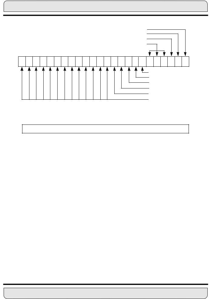
Figure 7-2 Timer/Event Counter Programming Model
The DSP56002 views the timer as a memory-mapped peripheral occupying two 24-bit words in the X data memory space, and may use it as a normal memory-mapped peripheral by using standard polled or interrupt programming techniques.The programming model is shown in Figure 7-2.
7.3TIMER COUNT REGISTER (TCR)
The 24-bit read-write TCR contains the value (specified by the user program) to be loaded into the counter when the timer is enabled (TE=1), or when the counter has been decremented to zero and a new event occurs. If the TCR is loaded with n, the counter will be reloaded after (n+1) events.
If the timer is disabled (TE=0) and the user program writes to the TCR, the value is stored there but will not be loaded into the counter until the timer becomes enabled. When the timer is enabled (TE=1) and the user program writes to the TCR, the value is stored there and will be loaded into the counter after the counter has been decremented to zero and a new event occurs.
In Timer Modes 4 and 5, however, the TCR will be loaded with the current value of the counter on the appropriate edge of the TIO input signal (rather than with a value specified by the user program). The value loaded to the TCR represents the width or the period of
7 - 4 DSP56002 TIMER AND EVENT COUNTER MOTOROLA
For More Information On This Product, Go to: www.freescale.com