- •Laboratory work № 6 – 10 studying of a photoeffect in a p-n junction
- •2_Main concepts
- •2.2 Photodiode properties
- •3 Description of laboratory research facility and methodology of measurements
- •4 Work execution order and experimental data analysis
- •5 Control questions
- •Laboratory work № 6-10 ι. Homework.
- •Ιι. Laboratory work № 6-10 implementation protocol.
- •Studying of a photoeffect in a p-n junction
- •5) Equations for calculation:
- •6) Table of measurements
Laboratory work № 6 – 10 studying of a photoeffect in a p-n junction
 Figure
27
–
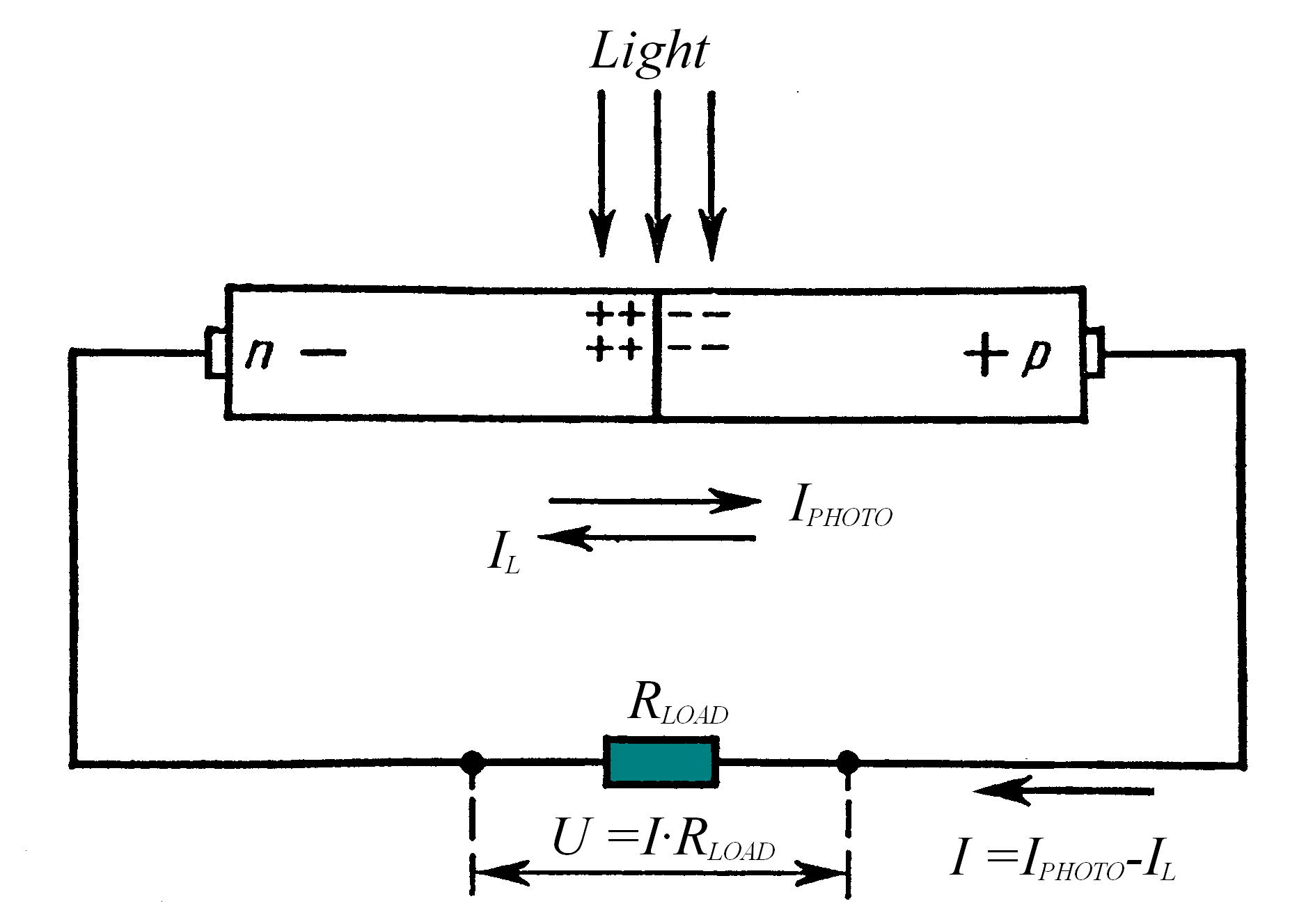
Principle of operation of the photocell.
Studying the photoeffect in a p-n junction and measuring of dark and light current-voltage characteristics.
2_Main concepts
2.1 P-N junction (see work 6-9)
2.2 Photodiode properties
Figure
25
–
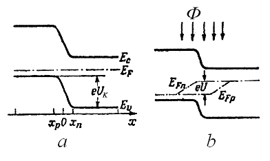
Band diagram of non-illuminated
(а)
and illuminated (b)
p-n junction.

hf0 = Eg,
that means that energy of photons hf0 must be not less than the forbidden energy gap width.
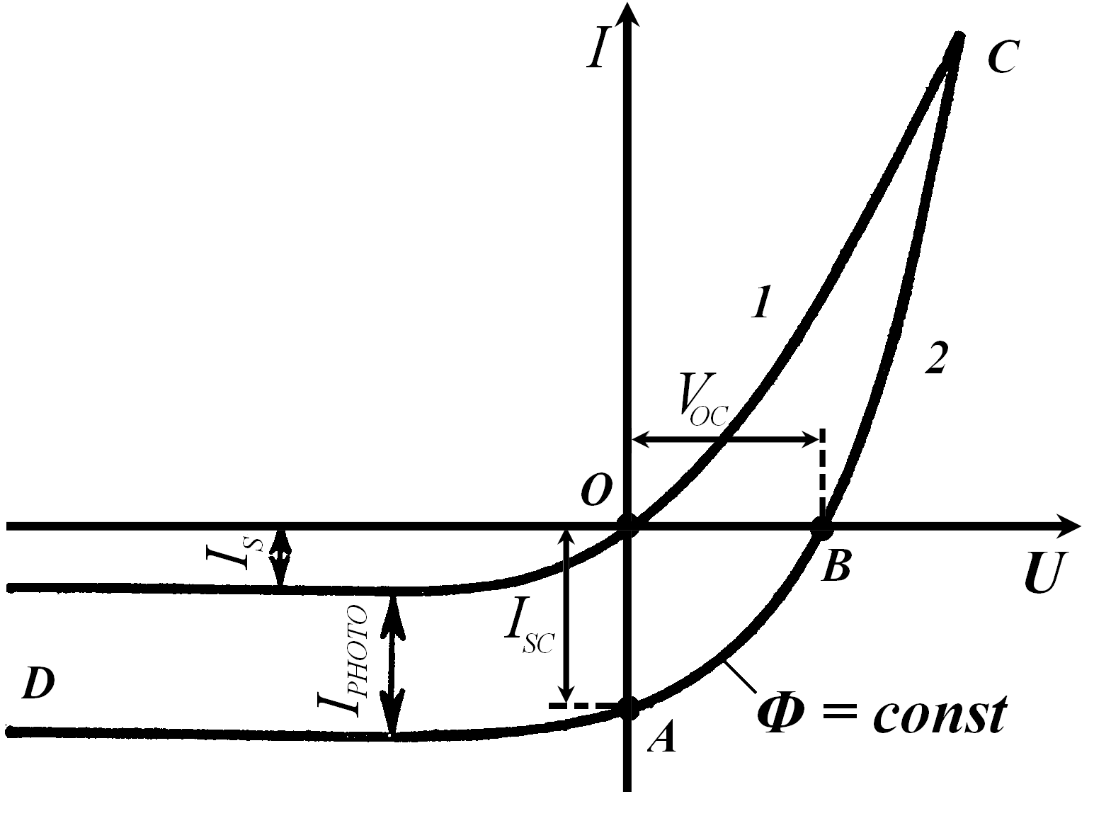
On the Fig. 26 (curve 1) represented current-voltage characteristic of non-illuminated p-n junction. It can be described by such equation:
|
(78) |
 Figure
26
–
CVC of the non-illuminated (curve 1) and illuminated (curve 2)
р-n-junction.
Now let’s p-n junction be illuminated by light with energy of photons not less then forbidden gap width of the semiconductor. The internal photoeffect will lead to generation of electron-hole pairs, concentration of which will decrease with increasing of distance from illuminated surface. Electrons and holes will move to the junction, where they will be separated. Majority carriers of the region will be held by internal built-in electric field. Accelerated minority carriers will freely path through p-n junction, and create photocurrent IPHOTO, which flows in the reverse direction (from n- to p - region).
If the circuit is open, then on the borders of p-n junction appears volume charge that opposes to further migration of charge carriers. This volume charge produces photo-emf U0 with polarity reverse to polarity of built-in potential. Potential barrier of depletion region decreases (Fig. 25b). That leads to appearance of leakage current IL flowing in the reverse direction. The photo-emf will be increased until the photocurrent will be compensated by increasing current of majority carriers.
If we connect to p-n junction load resistance RLOAD (Fig. 27), than, in obtained circuit will flow a current I which can be represented as:
I = IPHOTO - IL |
(79) |
Leakage current IL can be calculated by formula (78) for non-illuminated p-n junction when an external forward bias voltage ULOAD = IRLOAD is applied:
![]() .
.
Let’s consider the critical modes of operation of such photocell.
Short-circuit mode appears if RLOAD = 0. Then ULOAD = 0, IL = 0 and short circuit current ISC is equal to photocurrent IPHOTO which is proportional to light intensity Ф:
ISC = IPHOTO ; IPHOTO Ф
(80)
Open-circuit mode will take place if RLOAD = . The open-circuit voltage
VOC = UPHOTO, total current I = 0 and IPHOTO = IL. Equation (78) gives
|
(81) |
from where we get
|
(82) |
where UPHOTO – is a photo EMF generated in the photocell.
Thus, valve photocells allow to transform radiant energy directly into electric one. That is why they also called the photogalvanic elements and used as sources of EMF in the solar cell batteries.
 Figure
28
–
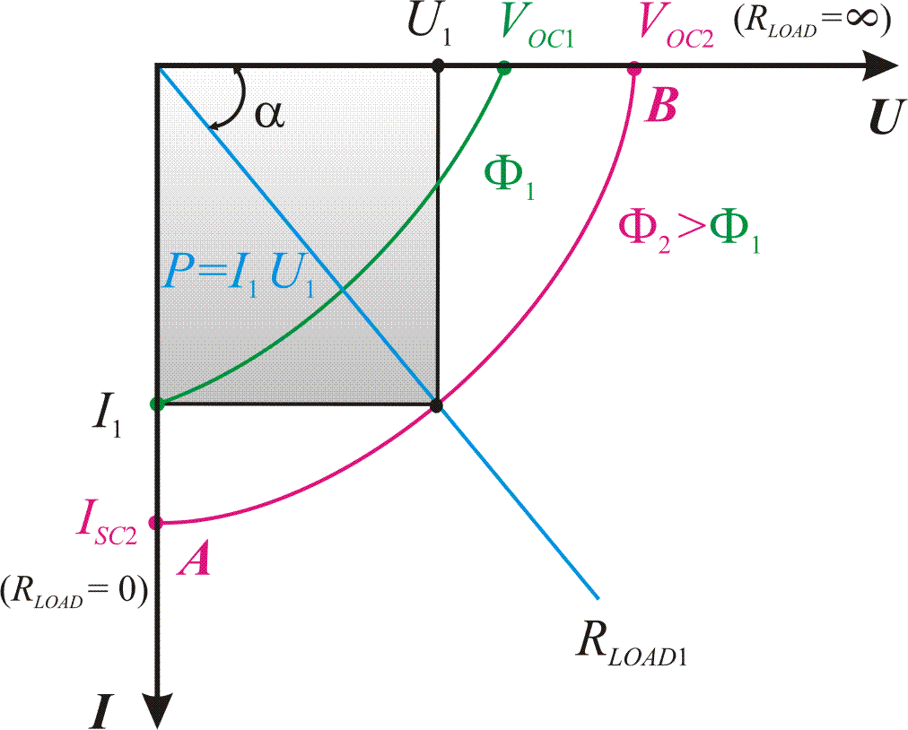
photocells’ CVC at different light intensities.
The
CVCs will be displaced and change their shape under the change of
light flux intensity. The photocell CVCs in a photogalvanic mode for
different light intensities are shown on the Fig.28. Straight line,
drawn from the coordinate origin under the angle α (![]() ),
intersects the CVC at point, which X coordinate is equal to voltage
drop on the load RLOAD , and Y coordinate –
current in the external circuit (for example U1 =
I1·RLOAD1).
Dashed area (Fig.28) is proportional to power P, generated on
the load RLOAD1:
),
intersects the CVC at point, which X coordinate is equal to voltage
drop on the load RLOAD , and Y coordinate –
current in the external circuit (for example U1 =
I1·RLOAD1).
Dashed area (Fig.28) is proportional to power P, generated on
the load RLOAD1:
|
(83) |
Optimal
load resistance
![]() chosen in such way that this power will be maximal.
Efficiency
of the photogalvanic cell η determined as:
chosen in such way that this power will be maximal.
Efficiency
of the photogalvanic cell η determined as:
|
(84) |
where Ф – light intensity in Watts, P – useful power, emitted on the load.
