
- •Features
- •Pin Configurations
- •Overview
- •Block Diagram
- •Disclaimer
- •Pin Descriptions
- •Port C (PC5..PC0)
- •PC6/RESET
- •Port D (PD7..PD0)
- •RESET
- •AVCC
- •AREF
- •AVR CPU Core
- •Introduction
- •Architectural Overview
- •Status Register
- •Stack Pointer
- •Interrupt Response Time
- •SRAM Data Memory
- •EEPROM Data Memory
- •EEPROM Read/Write Access
- •I/O Memory
- •Clock Systems and their Distribution
- •Clock Sources
- •Crystal Oscillator
- •External RC Oscillator
- •External Clock
- •Timer/Counter Oscillator
- •Idle Mode
- •Power-down Mode
- •Power-save Mode
- •Standby Mode
- •Analog Comparator
- •Brown-out Detector
- •Internal Voltage Reference
- •Watchdog Timer
- •Port Pins
- •Resetting the AVR
- •Reset Sources
- •Power-on Reset
- •External Reset
- •Brown-out Detection
- •Watchdog Reset
- •Watchdog Timer
- •Timed Sequences for Changing the Configuration of the Watchdog Timer
- •Interrupts
- •I/O Ports
- •Introduction
- •Configuring the Pin
- •Reading the Pin Value
- •Unconnected pins
- •Alternate Port Functions
- •Alternate Functions of Port B
- •Alternate Functions of Port C
- •Alternate Functions of Port D
- •Register Description for I/O Ports
- •External Interrupts
- •8-bit Timer/Counter0
- •Overview
- •Registers
- •Definitions
- •Counter Unit
- •Operation
- •Internal Clock Source
- •Prescaler Reset
- •External Clock Source
- •16-bit Timer/Counter1
- •Overview
- •Registers
- •Definitions
- •Compatibility
- •Counter Unit
- •Input Capture Unit
- •Input Capture Pin Source
- •Noise Canceler
- •Using the Input Capture Unit
- •Output Compare Units
- •Force Output Compare
- •Modes of Operation
- •Normal Mode
- •Fast PWM Mode
- •Phase Correct PWM Mode
- •8-bit Timer/Counter2 with PWM and Asynchronous Operation
- •Overview
- •Registers
- •Definitions
- •Counter Unit
- •Output Compare Unit
- •Force Output Compare
- •Modes of Operation
- •Normal Mode
- •Fast PWM Mode
- •Phase Correct PWM Mode
- •Timer/Counter Prescaler
- •SS Pin Functionality
- •Slave Mode
- •Master Mode
- •Data Modes
- •USART
- •Overview
- •Clock Generation
- •External Clock
- •Synchronous Clock Operation
- •Frame Formats
- •Parity Bit Calculation
- •USART Initialization
- •Sending Frames with 5 to 8 Data Bits
- •Sending Frames with 9 Data Bits
- •Parity Generator
- •Disabling the Transmitter
- •Receiving Frames with 5 to 8 Data Bits
- •Receiving Frames with 9 Data Bits
- •Receiver Error Flags
- •Parity Checker
- •Disabling the Receiver
- •Flushing the Receive Buffer
- •Asynchronous Data Recovery
- •Using MPCM
- •Write Access
- •Read Access
- •Two-wire Serial Interface
- •Features
- •TWI Terminology
- •Electrical Interconnection
- •Transferring Bits
- •START and STOP Conditions
- •Address Packet Format
- •Data Packet Format
- •Overview of the TWI Module
- •SCL and SDA Pins
- •Bit Rate Generator Unit
- •Bus Interface Unit
- •Address Match Unit
- •Control Unit
- •TWI Register Description
- •Using the TWI
- •Transmission Modes
- •Master Transmitter Mode
- •Master Receiver Mode
- •Slave Receiver Mode
- •Slave Transmitter Mode
- •Miscellaneous States
- •Analog Comparator
- •Analog Comparator Multiplexed Input
- •Features
- •Starting a Conversion
- •Changing Channel or Reference Selection
- •ADC Input Channels
- •ADC Voltage Reference
- •ADC Noise Canceler
- •Analog Input Circuitry
- •ADC Accuracy Definitions
- •ADC Conversion Result
- •ADLAR = 0
- •ADLAR = 1
- •Boot Loader Features
- •Application Section
- •Boot Loader Lock Bits
- •Performing a Page Write
- •Using the SPM Interrupt
- •Setting the Boot Loader Lock Bits by SPM
- •Reading the Fuse and Lock Bits from Software
- •Preventing Flash Corruption
- •Simple Assembly Code Example for a Boot Loader
- •Fuse Bits
- •Latching of Fuses
- •Signature Bytes
- •Calibration Byte
- •Page Size
- •Signal Names
- •Parallel Programming
- •Enter Programming Mode
- •Chip Erase
- •Programming the Flash
- •Programming the EEPROM
- •Reading the Flash
- •Reading the EEPROM
- •Programming the Lock Bits
- •Reading the Signature Bytes
- •Reading the Calibration Byte
- •Serial Downloading
- •Data Polling Flash
- •Data Polling EEPROM
- •Electrical Characteristics
- •Absolute Maximum Ratings*
- •DC Characteristics
- •External Clock Drive Waveforms
- •External Clock Drive
- •Two-wire Serial Interface Characteristics
- •ADC Characteristics
- •Active Supply Current
- •Idle Supply Current
- •Power-down Supply Current
- •Power-save Supply Current
- •Standby Supply Current
- •Pin Pull-up
- •Pin Driver Strength
- •Internal Oscillator Speed
- •Register Summary
- •Instruction Set Summary
- •Ordering Information
- •Packaging Information
- •Erratas
- •Changes from Rev. 2486N-09/04 to Rev. 2486O-10/04
- •Changes from Rev. 2486M-12/03 to Rev. 2486N-09/04
- •Changes from Rev. 2486L-10/03 to Rev. 2486M-12/03
- •Changes from Rev. 2486K-08/03 to Rev. 2486L-10/03
- •Changes from Rev. 2486J-02/03 to Rev. 2486K-08/03
- •Changes from Rev. 2486I-12/02 to Rev. 2486J-02/03
- •Changes from Rev. 2486H-09/02 to Rev. 2486I-12/02
- •Changes from Rev. 2486G-09/02 to Rev. 2486H-09/02
- •Changes from Rev. 2486F-07/02 to Rev. 2486G-09/02
- •Changes from Rev. 2486E-06/02 to Rev. 2486F-07/02
- •Changes from Rev. 2486D-03/02 to Rev. 2486E-06/02
- •Changes from Rev. 2486C-03/02 to Rev. 2486D-03/02
- •Changes from Rev. 2486B-12/01 to Rev. 2486C-03/02
- •Table of Contents

ATmega8(L)
ADC Characteristics
Table 103. |
ADC Characteristics |
|
|
|
|
|
|
|
|
Symbol |
Parameter |
Condition |
Min(1) |
Typ(1) |
|
Max(1) |
Units |
||
|
|
Resolution |
Single Ended Conversion |
|
10 |
|
|
|
Bits |
|
|
|
|
|
|
|
|
|
|
|
|
|
Single Ended Conversion |
|
|
|
|
|
|
|
|
Absolute accuracy |
VREF = 4V, VCC = 4V |
|
1.75 |
|
|
|
LSB |
|
|
(Including INL, DNL, |
ADC clock = 200 kHz |
|
|
|
|
|
|
|
|
|
|
|
|
|
|
|
|
|
|
Quantization Error, Gain, |
Single Ended Conversion |
|
|
|
|
|
|
|
|
and Offset Error) |
|
|
|
|
|
|
|
|
|
VREF = 4V, VCC = 4V |
|
3 |
|
|
|
LSB |
|
|
|
|
|
|
|
|
|||
|
|
|
ADC clock = 1 MHz |
|
|
|
|
|
|
|
|
|
|
|
|
|
|
|
|
|
|
|
Single Ended Conversion |
|
|
|
|
|
|
|
|
|
VREF = 4V, VCC = 4V |
|
|
|
|
|
|
|
|
Integral Non-linearity (INL) |
ADC clock = 200 kHz |
|
0.75 |
|
|
|
LSB |
|
|
|
|
|
|
|
|
|
|
|
|
|
Single Ended Conversion |
|
|
|
|
|
|
|
|
Differential Non-linearity |
VREF = 4V, VCC = 4V |
|
|
|
|
|
|
|
|
(DNL) |
ADC clock = 200 kHz |
|
0.5 |
|
|
|
LSB |
|
|
|
|
|
|
|
|
|
|
|
|
Gain Error |
Single Ended Conversion |
|
1 |
|
|
|
LSB |
|
|
|
VREF = 4V, VCC = 4V |
|
|
|
|
|
|
|
|
|
ADC clock = 200 kHz |
|
|
|
|
|
|
|
|
|
|
|
|
|
|
|
|
|
|
Offset Error |
Single Ended Conversion |
|
1 |
|
|
|
LSB |
|
|
|
VREF = 4V, VCC = 4V |
|
|
|
|
|
|
|
|
|
ADC clock = 200 kHz |
|
|
|
|
|
|
|
|
|
|
|
|
|
|
|
|
|
|
Conversion Time |
Free Running Conversion |
13 |
|
|
|
260 |
µs |
|
|
|
|
|
|
|
|
|
|
|
|
Clock Frequency |
|
50 |
|
|
1000 |
kHz |
|
|
|
|
|
|
|
|
|
|
|
AV |
CC |
Analog Supply Voltage |
|
V - 0.3(2) |
|
V |
CC |
+ 0.3(3) |
V |
|
|
|
CC |
|
|
|
|
||
VREF |
Reference Voltage |
|
2.0 |
|
|
AVCC |
V |
||
VIN |
Input voltage |
|
GND |
|
|
VREF |
V |
||
|
|
Input bandwidth |
|
|
38.5 |
|
|
|
kHz |
|
|
|
|
|
|
|
|
|
|
VINT |
Internal Voltage Reference |
|
2.3 |
2.56 |
|
|
2.7 |
V |
|
RREF |
Reference Input Resistance |
|
|
32 |
|
|
|
kΩ |
|
RAIN |
Analog Input Resistance |
|
55 |
100 |
|
|
|
MΩ |
Notes: 1. Values are guidelines only.
2.Minimum for AVCC is 2.7V.
3.Maximum for AVCC is 5.5V.
245
2486O–AVR–10/04

ATmega8 Typical
Characteristics
Active Supply Current
The following charts show typical behavior. These figures are not tested during manufacturing. All current consumption measurements are performed with all I/O pins configured as inputs and with internal pull-ups enabled. A sine wave generator with Rail- to-Rail output is used as clock source.
The power consumption in Power-down mode is independent of clock selection.
The current consumption is a function of several factors such as: operating voltage, operating frequency, loading of I/O pins, switching rate of I/O pins, code executed and ambient temperature. The dominating factors are operating voltage and frequency.
The current drawn from capacitive loaded pins may be estimated (for one pin) as CL*VCC*f where CL = load capacitance, VCC = operating voltage and f = average switching frequency of I/O pin.
The parts are characterized at frequencies higher than test limits. Parts are not guaranteed to function properly at frequencies higher than the ordering code indicates.
The difference between current consumption in Power-down mode with Watchdog Timer enabled and Power-down mode with Watchdog Timer disabled represents the differential current drawn by the Watchdog Timer.
Figure 118. Active Supply Current vs. Frequency (0.1 - 1.0 MHz)
ACTIVE SUPPLY CURRENT vs. FREQUENCY
|
|
|
|
|
|
0.1 - 1.0 MHz |
|
|
|
|
|
|
3 |
|
|
|
|
|
|
|
|
|
|
|
2.5 |
|
|
|
|
|
|
|
|
|
5.5V |
|
|
|
|
|
|
|
|
|
|
5.0V |
|
|
|
|
|
|
|
|
|
|
|
|
|
|
|
|
|
|
|
|
|
|
|
|
4.5V |
|
2 |
|
|
|
|
|
|
|
|
|
4.0V |
(mA) |
|
|
|
|
|
|
|
|
|
|
3.3V |
1.5 |
|
|
|
|
|
|
|
|
|
3.0V |
|
|
|
|
|
|
|
|
|
|
2.7V |
||
CC |
|
|
|
|
|
|
|
|
|
|
|
|
|
|
|
|
|
|
|
|
|
|
|
I |
|
|
|
|
|
|
|
|
|
|
|
|
1 |
|
|
|
|
|
|
|
|
|
|
|
0.5 |
|
|
|
|
|
|
|
|
|
|
|
0 |
|
|
|
|
|
|
|
|
|
|
|
0 |
0.1 |
0.2 |
0.3 |
0.4 |
0.5 |
0.6 |
0.7 |
0.8 |
0.9 |
1 |
Frequency (MHz)
246 ATmega8(L)
2486O–AVR–10/04

ATmega8(L)
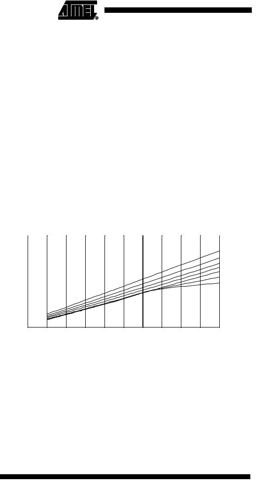
Figure 119. Active Supply Current vs. Frequency (1 - 20 MHz)
ACTIVE SUPPLY CURRENT vs. FREQUENCY
|
|
|
|
|
|
1 - 20 MHz |
|
|
|
|
|
|
30 |
|
|
|
|
|
|
|
|
|
|
|
|
|
|
|
|
|
|
|
|
|
5.5V |
|
25 |
|
|
|
|
|
|
|
|
|
5.0V |
|
|
|
|
|
|
|
|
|
|
|
|
|
20 |
|
|
|
|
|
|
|
|
|
4.5V |
|
|
|
|
|
|
|
|
|
|
|
|
(mA) |
15 |
|
|
|
|
|
|
|
|
|
|
CC |
|
|
|
|
|
|
|
|
|
|
|
I |
|
|
|
|
|
|
|
|
|
|
|
|
10 |
|
|
|
|
|
|
|
3.3V |
|
|
|
|
|
|
|
|
|
|
|
|
|
|
|
5 |
|
|
|
|
|
3.0V |
|
|
|
|
|
|
|
|
|
|
|
|
|
|
|
|
|
|
|
|
|
|
2.7V |
|
|
|
|
|
|
0 |
|
|
|
|
|
|
|
|
|
|
|
0 |
2 |
4 |
6 |
8 |
10 |
12 |
14 |
16 |
18 |
20 |
Frequency (MHz)
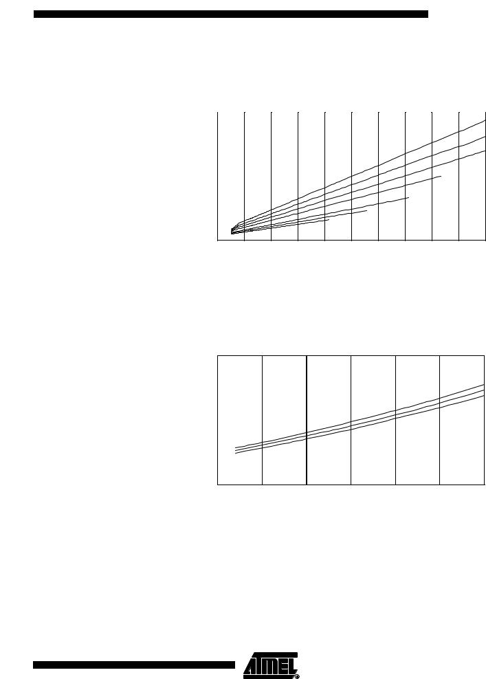
Figure 120. Active Supply Current vs. VCC (Internal RC Oscillator, 8 MHz)
ACTIVE SUPPLY CURRENT vs. VCC
INTERNAL RC OSCILLATOR, 8 MHz
|
18 |
|
|
|
|
|
|
|
16 |
|
|
|
|
|
|
|
14 |
|
|
|
|
|
-40°C |
|
|
|
|
|
|
25°C |
|
|
|
|
|
|
|
|
|
|
12 |
|
|
|
|
|
85°C |
(mA) |
10 |
|
|
|
|
|
|
|
|
|
|
|
|
|
|
CC |
8 |
|
|
|
|
|
|
I |
|
|
|
|
|
|
|
|
6 |
|
|
|
|
|
|
|
4 |
|
|
|
|
|
|
|
2 |
|
|
|
|
|
|
|
0 |
|
|
|
|
|
|
|
2.5 |
3 |
3.5 |
4 |
4.5 |
5 |
5.5 |
VCC (V)
247
2486O–AVR–10/04

Figure 121. Active Supply Current vs. VCC (Internal RC Oscillator, 4 MHz)
ACTIVE SUPPLY CURRENT vs. VCC
INTERNAL RC OSCILLATOR, 4 MHz
|
12 |
|
|
|
|
|
|
|
10 |
|
|
|
|
|
|
|
|
|
|
|
|
|
-40°C |
|
8 |
|
|
|
|
|
25°C |
(mA) |
|
|
|
|
|
|
85°C |
6 |
|
|
|
|
|
|
|
CC |
|
|
|
|
|
|
|
I |
|
|
|
|
|
|
|
|
4 |
|
|
|
|
|
|
|
2 |
|
|
|
|
|
|
|
0 |
|
|
|
|
|
|
|
2.5 |
3 |
3.5 |
4 |
4.5 |
5 |
5.5 |
VCC (V)
Figure 122. Active Supply Current vs. VCC (Internal RC Oscillator, 2 MHz)
ACTIVE SUPPLY CURRENT vs. VCC
INTERNAL RC OSCILLATOR, 2 MHz
|
6 |
|
|
|
|
|
|
|
|
|
|
|
|
|
25°C |
|
5 |
|
|
|
|
|
-40°C |
|
|
|
|
|
|
|
85°C |
|
4 |
|
|
|
|
|
|
(mA) |
3 |
|
|
|
|
|
|
CC |
|
|
|
|
|
|
|
I |
|
|
|
|
|
|
|
|
2 |
|
|
|
|
|
|
|
1 |
|
|
|
|
|
|
|
0 |
|
|
|
|
|
|
|
2.5 |
3 |
3.5 |
4 |
4.5 |
5 |
5.5 |
VCC (V)
248 ATmega8(L)
2486O–AVR–10/04

ATmega8(L)
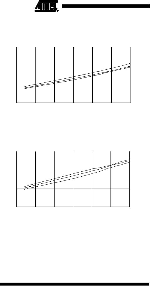
Figure 123. Active Supply Current vs. VCC (Internal RC Oscillator, 1 MHz)
ACTIVE SUPPLY CURRENT vs. VCC
INTERNAL RC OSCILLATOR, 1 MHz
|
3.5 |
|
|
|
|
|
|
|
|
3 |
|
|
|
|
|
|
85°C |
|
|
|
|
|
|
|
25°C |
|
|
|
|
|
|
|
|
|
|
|
2.5 |
|
|
|
|
|
-40°C |
|
|
|
|
|
|
|
|
|
|
(mA) |
2 |
|
|
|
|
|
|
|
|
|
|
|
|
|
|
|
|
CC |
1.5 |
|
|
|
|
|
|
|
I |
|
|
|
|
|
|
|
|
|
|
|
|
|
|
|
|
|
|
1 |
|
|
|
|
|
|
|
|
0.5 |
|
|
|
|
|
|
|
|
0 |
|
|
|
|
|
|
|
|
2.5 |
3 |
3.5 |
4 |
4.5 |
5 |
|
5.5 |
VCC (V)
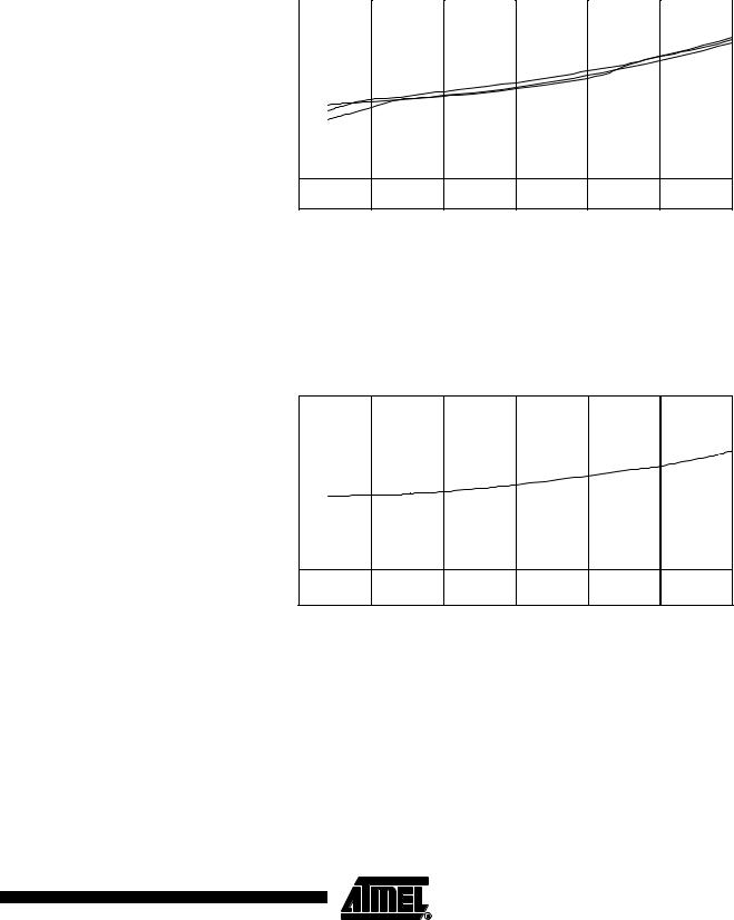
Figure 124. Active Supply Current vs. VCC (32 kHz External Oscillator)
ACTIVE SUPPLY CURRENT vs. VCC
32kHz EXTERNAL OSCILLATOR
|
120 |
|
|
|
|
|
|
|
100 |
|
|
|
|
|
|
|
|
|
|
|
|
|
25°C |
|
80 |
|
|
|
|
|
|
(uA) |
60 |
|
|
|
|
|
|
CC |
|
|
|
|
|
|
|
|
|
|
|
|
|
|
|
I |
|
|
|
|
|
|
|
|
40 |
|
|
|
|
|
|
|
20 |
|
|
|
|
|
|
|
0 |
|
|
|
|
|
|
|
2.5 |
3 |
3.5 |
4 |
4.5 |
5 |
5.5 |
VCC (V)
249
2486O–AVR–10/04