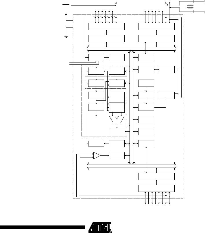
- •Features
- •Pin Configurations
- •Overview
- •Block Diagram
- •Disclaimer
- •Pin Descriptions
- •Port C (PC5..PC0)
- •PC6/RESET
- •Port D (PD7..PD0)
- •RESET
- •AVCC
- •AREF
- •AVR CPU Core
- •Introduction
- •Architectural Overview
- •Status Register
- •Stack Pointer
- •Interrupt Response Time
- •SRAM Data Memory
- •EEPROM Data Memory
- •EEPROM Read/Write Access
- •I/O Memory
- •Clock Systems and their Distribution
- •Clock Sources
- •Crystal Oscillator
- •External RC Oscillator
- •External Clock
- •Timer/Counter Oscillator
- •Idle Mode
- •Power-down Mode
- •Power-save Mode
- •Standby Mode
- •Analog Comparator
- •Brown-out Detector
- •Internal Voltage Reference
- •Watchdog Timer
- •Port Pins
- •Resetting the AVR
- •Reset Sources
- •Power-on Reset
- •External Reset
- •Brown-out Detection
- •Watchdog Reset
- •Watchdog Timer
- •Timed Sequences for Changing the Configuration of the Watchdog Timer
- •Interrupts
- •I/O Ports
- •Introduction
- •Configuring the Pin
- •Reading the Pin Value
- •Unconnected pins
- •Alternate Port Functions
- •Alternate Functions of Port B
- •Alternate Functions of Port C
- •Alternate Functions of Port D
- •Register Description for I/O Ports
- •External Interrupts
- •8-bit Timer/Counter0
- •Overview
- •Registers
- •Definitions
- •Counter Unit
- •Operation
- •Internal Clock Source
- •Prescaler Reset
- •External Clock Source
- •16-bit Timer/Counter1
- •Overview
- •Registers
- •Definitions
- •Compatibility
- •Counter Unit
- •Input Capture Unit
- •Input Capture Pin Source
- •Noise Canceler
- •Using the Input Capture Unit
- •Output Compare Units
- •Force Output Compare
- •Modes of Operation
- •Normal Mode
- •Fast PWM Mode
- •Phase Correct PWM Mode
- •8-bit Timer/Counter2 with PWM and Asynchronous Operation
- •Overview
- •Registers
- •Definitions
- •Counter Unit
- •Output Compare Unit
- •Force Output Compare
- •Modes of Operation
- •Normal Mode
- •Fast PWM Mode
- •Phase Correct PWM Mode
- •Timer/Counter Prescaler
- •SS Pin Functionality
- •Slave Mode
- •Master Mode
- •Data Modes
- •USART
- •Overview
- •Clock Generation
- •External Clock
- •Synchronous Clock Operation
- •Frame Formats
- •Parity Bit Calculation
- •USART Initialization
- •Sending Frames with 5 to 8 Data Bits
- •Sending Frames with 9 Data Bits
- •Parity Generator
- •Disabling the Transmitter
- •Receiving Frames with 5 to 8 Data Bits
- •Receiving Frames with 9 Data Bits
- •Receiver Error Flags
- •Parity Checker
- •Disabling the Receiver
- •Flushing the Receive Buffer
- •Asynchronous Data Recovery
- •Using MPCM
- •Write Access
- •Read Access
- •Two-wire Serial Interface
- •Features
- •TWI Terminology
- •Electrical Interconnection
- •Transferring Bits
- •START and STOP Conditions
- •Address Packet Format
- •Data Packet Format
- •Overview of the TWI Module
- •SCL and SDA Pins
- •Bit Rate Generator Unit
- •Bus Interface Unit
- •Address Match Unit
- •Control Unit
- •TWI Register Description
- •Using the TWI
- •Transmission Modes
- •Master Transmitter Mode
- •Master Receiver Mode
- •Slave Receiver Mode
- •Slave Transmitter Mode
- •Miscellaneous States
- •Analog Comparator
- •Analog Comparator Multiplexed Input
- •Features
- •Starting a Conversion
- •Changing Channel or Reference Selection
- •ADC Input Channels
- •ADC Voltage Reference
- •ADC Noise Canceler
- •Analog Input Circuitry
- •ADC Accuracy Definitions
- •ADC Conversion Result
- •ADLAR = 0
- •ADLAR = 1
- •Boot Loader Features
- •Application Section
- •Boot Loader Lock Bits
- •Performing a Page Write
- •Using the SPM Interrupt
- •Setting the Boot Loader Lock Bits by SPM
- •Reading the Fuse and Lock Bits from Software
- •Preventing Flash Corruption
- •Simple Assembly Code Example for a Boot Loader
- •Fuse Bits
- •Latching of Fuses
- •Signature Bytes
- •Calibration Byte
- •Page Size
- •Signal Names
- •Parallel Programming
- •Enter Programming Mode
- •Chip Erase
- •Programming the Flash
- •Programming the EEPROM
- •Reading the Flash
- •Reading the EEPROM
- •Programming the Lock Bits
- •Reading the Signature Bytes
- •Reading the Calibration Byte
- •Serial Downloading
- •Data Polling Flash
- •Data Polling EEPROM
- •Electrical Characteristics
- •Absolute Maximum Ratings*
- •DC Characteristics
- •External Clock Drive Waveforms
- •External Clock Drive
- •Two-wire Serial Interface Characteristics
- •ADC Characteristics
- •Active Supply Current
- •Idle Supply Current
- •Power-down Supply Current
- •Power-save Supply Current
- •Standby Supply Current
- •Pin Pull-up
- •Pin Driver Strength
- •Internal Oscillator Speed
- •Register Summary
- •Instruction Set Summary
- •Ordering Information
- •Packaging Information
- •Erratas
- •Changes from Rev. 2486N-09/04 to Rev. 2486O-10/04
- •Changes from Rev. 2486M-12/03 to Rev. 2486N-09/04
- •Changes from Rev. 2486L-10/03 to Rev. 2486M-12/03
- •Changes from Rev. 2486K-08/03 to Rev. 2486L-10/03
- •Changes from Rev. 2486J-02/03 to Rev. 2486K-08/03
- •Changes from Rev. 2486I-12/02 to Rev. 2486J-02/03
- •Changes from Rev. 2486H-09/02 to Rev. 2486I-12/02
- •Changes from Rev. 2486G-09/02 to Rev. 2486H-09/02
- •Changes from Rev. 2486F-07/02 to Rev. 2486G-09/02
- •Changes from Rev. 2486E-06/02 to Rev. 2486F-07/02
- •Changes from Rev. 2486D-03/02 to Rev. 2486E-06/02
- •Changes from Rev. 2486C-03/02 to Rev. 2486D-03/02
- •Changes from Rev. 2486B-12/01 to Rev. 2486C-03/02
- •Table of Contents

ATmega8(L)
Overview
Block Diagram
The ATmega8 is a low-power CMOS 8-bit microcontroller based on the AVR RISC architecture. By executing powerful instructions in a single clock cycle, the ATmega8 achieves throughputs approaching 1 MIPS per MHz, allowing the system designer to optimize power consumption versus processing speed.
Figure 1. |
Block Diagram |
|
|
|
|
|
|
|
XTAL1 |
RESET |
|
|
|
|
|
PC0 - PC6 |
|
|
PB0 - PB7 |
VCC |
|
|
|
XTAL2 |
|
|
|
|
|
|
PORTC DRIVERS/BUFFERS |
PORTB DRIVERS/BUFFERS |
||
GND |
PORTC DIGITAL INTERFACE |
PORTB DIGITAL INTERFACE |
||
|
|
|
|
|
|
MUX & |
ADC |
TWI |
|
|
ADC |
INTERFACE |
|
|
|
|
|
||
AGND |
|
|
|
|
AREF |
|
|
|
|
|
PROGRAM |
STACK |
TIMERS/ |
OSCILLATOR |
|
COUNTERS |
|||
|
COUNTER |
POINTER |
|
|
|
|
|
||
|
PROGRAM |
SRAM |
INTERNAL |
|
|
FLASH |
OSCILLATOR |
|
|
|
|
|
||
|
INSTRUCTION |
GENERAL |
WATCHDOG |
OSCILLATOR |
|
REGISTER |
PURPOSE |
TIMER |
|
|
|
|||
|
|
|
|
|
|
|
REGISTERS |
|
|
|
X |
|
|
INSTRUCTION |
Y |
MCU CTRL. |
|
DECODER |
& TIMING |
||
|
|||
|
Z |
|
|
CONTROL |
|
INTERRUPT |
|
LINES |
ALU |
UNIT |
|
AVR CPU |
STATUS |
EEPROM |
|
REGISTER |
|||
|
|
||
PROGRAMMING |
SPI |
USART |
|
LOGIC |
|||
|
|
||
+ |
COMP. |
|
|
- |
INTERFACE |
|
PORTD DIGITAL INTERFACE
PORTD DRIVERS/BUFFERS
PD0 - PD7
3
2486O–AVR–10/04

|
|
|
|
|
|
|
|
|
|
|
|
|
The AVR core combines a rich instruction set with 32 general purpose working registers. |
||||
|
All the 32 registers are directly connected to the Arithmetic Logic Unit (ALU), allowing |
||||
|
two independent registers to be accessed in one single instruction executed in one clock |
||||
|
cycle. The resulting architecture is more code efficient while achieving throughputs up to |
||||
|
ten times faster than conventional CISC microcontrollers. |
||||
|
The ATmega8 provides the following features: 8K bytes of In-System Programmable |
||||
|
Flash with Read-While-Write capabilities, 512 bytes of EEPROM, 1K byte of SRAM, 23 |
||||
|
general purpose I/O lines, 32 general purpose working registers, three flexible |
||||
|
Timer/Counters with compare modes, internal and external interrupts, a serial program- |
||||
|
mable USART, a byte oriented Two-wire Serial Interface, a 6-channel ADC (eight |
||||
|
channels in TQFP and MLF packages) with 10-bit accuracy, a programmable Watchdog |
||||
|
Timer with Internal Oscillator, an SPI serial port, and five software selectable power sav- |
||||
|
ing modes. The Idle mode stops the CPU while allowing the SRAM, Timer/Counters, |
||||
|
SPI port, and interrupt system to continue functioning. The Power-down mode saves the |
||||
|
register contents but freezes the Oscillator, disabling all other chip functions until the |
||||
|
next Interrupt or Hardware Reset. In Power-save mode, the asynchronous timer contin- |
||||
|
ues to run, allowing the user to maintain a timer base while the rest of the device is |
||||
|
sleeping. The ADC Noise Reduction mode stops the CPU and all I/O modules except |
||||
|
asynchronous timer and ADC, to minimize switching noise during ADC conversions. In |
||||
|
Standby mode, the crystal/resonator Oscillator is running while the rest of the device is |
||||
|
sleeping. This allows very fast start-up combined with low-power consumption. |
||||
|
The device is manufactured using Atmel’s high density non-volatile memory technology. |
||||
|
The Flash Program memory can be reprogrammed In-System through an SPI serial |
||||
|
interface, by a conventional non-volatile memory programmer, or by an On-chip boot |
||||
|
program running on the AVR core. The boot program can use any interface to download |
||||
|
the application program in the Application Flash memory. Software in the Boot Flash |
||||
|
Section will continue to run while the Application Flash Section is updated, providing |
||||
|
true Read-While-Write operation. By combining an 8-bit RISC CPU with In-System Self- |
||||
|
Programmable Flash on a monolithic chip, the Atmel ATmega8 is a powerful microcon- |
||||
|
troller that provides a highly-flexible and cost-effective solution to many embedded |
||||
|
control applications. |
||||
|
The ATmega8 AVR is supported with a full suite of program and system development |
||||
|
tools, including C compilers, macro assemblers, program debugger/simulators, In-Cir- |
||||
|
cuit Emulators, and evaluation kits. |
||||
Disclaimer |
Typical values contained in this datasheet are based on simulations and characteriza- |
||||
|
tion of other AVR microcontrollers manufactured on the same process technology. Min |
||||
|
and Max values will be available after the device is characterized. |
4 ATmega8(L)
2486O–AVR–10/04