

Neoway M590
.pdfNeo_M590
Hardware Design
Manual
Version 1.1
Let's enjoy the wireless life!

Neo_M590 Hardware Design Manual |
V1.1 |
Copyright Statement
Copyright © 2008 Neoway Tech
All rights reserved by Shenzhen Neoway Technology Co.,Ltd.
The trademark  belongs to Shenzhen Neoway Technology Co.,Ltd. Other trademarks in this manual belong to their owners.
Clarification
This specification applies to the M590.
This specification is for system engineers, research engineers and test engineers.
This specification is, without prior notice, subject to changes and updates as deemed neccesary by Neoway to suit enhancements or changes to the module.
All statements, information and suggestions in this manual do not constitute any express or implied guarantees.
Shenzhen Neoway Technology Co.,Ltd can supply technological support.
For querries contact your sales representative or send E-mail to these two mailboxs: sales@neoway.com.cn
support@neoway.com.cn Website: www.neoway.com.cn
Copyright © Shenzhen Neoway Tech Co,.Ltd |
Page 2 of 29 |

Neo_M590 Hardware Design Manual |
V1.1 |
|
|
|
Contents |
|
1. |
OVERVIEW................................................................................................................................. |
5 |
||
2. |
CONFIGURATION..................................................................................................................... |
5 |
||
3. |
DESIGN DIAGRAM ................................................................................................................... |
5 |
||
4. |
FEATURES ................................................................................................................................. |
6 |
||
5. |
PIN DEFINITION........................................................................................................................ |
6 |
||
6. |
INTERFACE DESIGN REFERENCE...................................................................................... |
8 |
||
|
6.1 |
POWER SUPPLY & AND RESET INTERFACE................................................................................................. |
8 |
|
|
|
6.1.1 |
Power Supply ..................................................................................................................... |
8 |
|
|
6.1.2 |
Power on/off Sequencing................................................................................................. |
12 |
|
|
6.1.3 |
Pin Description................................................................................................................. |
13 |
|
|
6.1.4 |
Module Abnormality Recovery ........................................................................................ |
14 |
|
|
6.1.5 |
VCCIO Pin Description ...................................................................................................... |
16 |
|
6.2 |
SERIAL INTERFACE ............................................................................................................................. |
16 |
|
|
6.3 |
SIM CARD INTERFACE ........................................................................................................................ |
19 |
|
|
6.4 |
INDICATOR LIGHT (LED) ..................................................................................................................... |
21 |
|
|
6.5 |
RF CONNECTOR ................................................................................................................................ |
21 |
|
|
6.6 |
SIGNAL CONNECTOR AND PCB PACKING ................................................................................................ |
22 |
|
7. |
ASSEMBLY............................................................................................................................... |
26 |
||
8. |
PACKAGING............................................................................................................................. |
26 |
||
9. |
ABBREVIATIONS .................................................................................................................... |
27 |
||
10. APPENDIX 1.DESCRIPTION OF THE M590 SLEEP MODE........................................... |
28 |
|||
Copyright © Shenzhen Neoway Tech Co,.Ltd |
Page 3 of 29 |

Neo_M590 Hardware Design Manual |
V1.1 |
Revision History
Version |
Content Revised |
Effective time |
|
|
|
V1.0 |
Initial version |
201004 |
V1.1 |
Revised version,improved the design following |
201108 |
|
customers feedback |
|
Copyright © Shenzhen Neoway Tech Co,.Ltd |
Page 4 of 29 |
Neo_M590 Hardware Design Manual |
V1.1 |
1. Overview
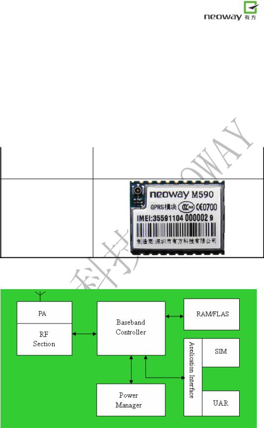
M590 pure-data Communication Module is an ultra compact GSM/GPRS industrial wireless module, optional Dual-band or Quad-band. It provides a high-quality SMS, GPRS data connection for use in industrial and commercial fields.
2. Configuration
|
|
Table 1 Shape of M590 |
|
|
|
|
|
|
Specifications |
Description |
|
|
Dimensions |
27.6mm*21.6mm*2.6mm (length*width*height) |
|
|
Weight |
5g |
|
Overview
3. Design Diagram
Copyright © Shenzhen Neoway Tech Co,.Ltd |
Page 5 of 29 |

Neo_M590 Hardware Design Manual |
V1.1 |
4. Features
|
Table 2 Main Specifications of M590 |
|
|
|
|
Specification |
|
Description |
Frequency bands |
|
EGSM900/DCS1800 Dual-band, or GSM850/1900 or |
|
Quad-band |
|
|
|
|
Sensitivity |
|
-107dBm |
Maximum Transmission |
|
EGSM900 Class4(2W) |
Power |
|
DCS1800 Class1(1W) |
Instantaneous Current |
|
Max 2A |
Operating Current |
|
210mA |
Sleep mode Current |
|
2.5mA |
Working Temperature |
|
-40 +85 |
Operating Voltage |
|
3.3V 4.5V The recommend value is 3.9V |
Protocol |
|
Compatible with GSM/GPRS Phase2/2+, increased |
|
TCP/IP, FTP, UDP etc. |
|
|
|
|
AT |
|
GSM07.07 |
|
Extended command sets |
|
|
|
|
Connector |
|
20 pins LLC,20 pin DIL form factor |
|
Murata GSC RF connector, or pad on board |
|
|
|
|
SMS |
|
TEXT/PDU |
|
Point to point/cell broadcast |
|
|
|
|
Grouped Data |
|
GPRS CLASS 10 |
|
Coding mode: CS1 CS2 CS3 CS4 |
|
|
|
|
Circuit Switched Data |
|
Supports CSD data service |
|
Supports USSD |
|
|
|
|
5. Pin Definition
Table 3 Pin Definition of M590
|
Pin |
|
Signal |
|
I/O |
|
|
Description of functions |
|
|
Remark |
|
|
|
|
Name |
|
|
|
|
|
|
|||||
|
|
|
|
|
|
|
|
|
|
|
|
|
|
1 |
|
GND |
|
PWR |
|
Ground |
|
|
|
|
|||
2-3 |
|
VBAT |
|
PWR |
|
VCC_MAIN input |
|
|
|
|
|||
4 |
|
GND |
|
PWR |
|
Ground |
|
|
|
|
|||
5 |
|
LED |
|
O |
|
Indicating working status |
|
|
|
|
|||
6 |
|
VCCIO |
|
O |
|
2.85V interface level output |
|
IO reference |
Level, load |
||||
|
|
|
|
|
|
|
|
|
capacity<3mA |
|
|
||
|
|
|
|
|
|
|
|
|
|
|
|
|
|
7 |
|
RXD |
|
I |
|
Receiving Data |
|
Maximum level |
is < 3.3V |
||||
Copyright © Shenzhen Neoway Tech Co,.Ltd |
Page 6 of 29 |

Neo_M590 Hardware Design Manual |
V1.1 |
|
|
|
|
|
|
||||
|
|
|
|
|
|
|
|
||||
8 |
TXD |
|
O |
Sending Data |
|
High level 2.85V output |
|
||||
9 |
DTR |
|
I |
User Circuit Ready |
|
|
|
|
|
|
|
10 |
RING |
|
O |
Ring |
|
|
High level 2.85V output |
|
|||
11 |
SIMIO |
|
I/O |
SIM card data |
|
Need to pull up to SIMVCC |
|
||||
|
|
|
|
|
|
by external resistance 10K |
|
||||
|
|
|
|
|
|
|
|
||||
12 |
SIMCLK |
|
O |
SIM card clock |
|
|
|
|
|
|
|
13 |
SIMRST |
|
O |
SIM card reset |
|
|
|
|
|
|
|
14 |
SIMVCC |
|
PWR |
SIM card power output |
|
|
|
|
|
|
|
15 |
GND |
|
PWR |
Ground |
|
|
|
|
|
|
|
16 |
DCD |
|
O |
Data Carrier Detect |
|
Not supported,0V output |
|
||||
17 |
DSR |
|
O |
The module ready |
|
Not supported,2.85V output |
|
||||
|
EMERGOFF |
|
I/O |
Emergency power OFF |
|
Internally |
pulled |
up to |
|
||
18 |
|
|
|
|
|
|
VCCRTC, |
do |
not |
apply |
|
|
|
|
|
|
|
|
voltage over 2.0V |
|
|
||
|
ON/OFF |
|
I |
ON/OFF control |
|
Active low. |
For |
more |
|
||
19 |
|
|
|
|
|
|
instruction |
please |
referto |
|
|
|
|
|
|
|
|
ON/OFF/RESET |
|
|
|||
|
|
|
|
|
|
|
|
|
|||
|
|
|
|
|
|
|
instruction. |
|
|
|
|
20 |
GND |
|
PWR |
Ground |
|
|
|
|
|
|
|
21 |
RF_ANT |
|
I/O |
RF input/output |
|
|
|
|
|
|
|
Other pads are test pads, please keep corresponding area clear of copper, to prevent short |
|
||||||||||
circuit when mounting. |
|
|
|
|
|
|
|
|
|
||
Notice |
|
|
|
|
|
|
|
|
|
||
Because the module uses a 2.85V IO power system, |
maximum input voltage of all IO |
|
|||||||||
interfaces can not exceed 3.3V, otherwise the IO may be damaged.IO interfaces with a 3.3V
power supply may for various reasons output at 3.3V or higher. In this event, this voltage on
the I/O signal interface will connect to the IO of the 2.85V module and damage the IO ports.
Resistors in series with these ports should be used, as well as capacitors and filters. For
further details refer to item 6.2.
Copyright © Shenzhen Neoway Tech Co,.Ltd |
Page 7 of 29 |

Neo_M590 Hardware Design Manual |
V1.1 |
6. Interface Design Reference
6.1 Power Supply & and Reset Interface
Table 4 Power Supply & and Reset Interface
|
Pin |
|
|
Signal Name |
|
|
I/O |
|
Description of |
|
Remark |
|
|
|
|
|
|
|
Functions |
|
|
||||
|
|
|
|
|
|
|
|
|
|
|
|
|
1,4,15,20 |
|
|
GND |
|
PWR |
Ground |
|
|
|
|||
2,3 |
|
|
VBAT |
|
PWR |
VCC_MAIN input |
|
|
|
|||
6 |
|
|
VCCIO |
|
O |
2.85V interface level |
|
IO reference Level, load |
||||
|
|
|
output |
|
capacity<3mA |
|||||||
|
|
|
|
|
|
|
|
|
|
|||
18 |
|
|
EMERGOFF |
|
I/O |
Emergency Power OFF |
|
Active low, 10us |
||||
19 |
|
|
ON/OFF |
|
I |
ON/OFF control |
|
Active low, 300ms |
||||
6.1.1 Power Supply
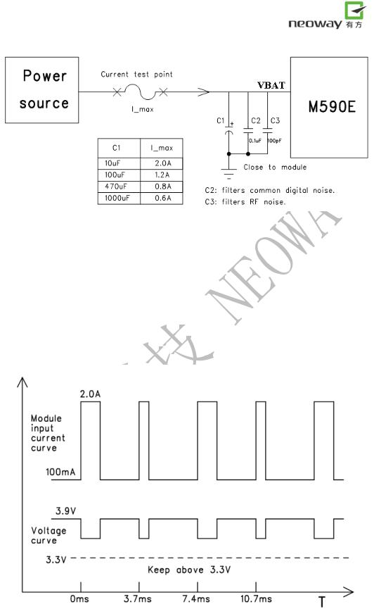
Power supply design and good PCB design techniques are crucial for ideal performance of the module. The power source not only powers the digital and analog circuit, but also the RF power amplifier which draws high peak currents. It is necessary to include low ESR electrolytic capacitors and/or tantalum capacitors, close to the VBAT supply inputs (Pin2 and Pin3). Further to this, filtering capacitors in the range of 0.1uF, 100pF and 33pF should also be included for higher frequency interference reduction.
VBAT (Pin2 and 3) is the main power supply of the module, with input range of 3.3V to 4.8V, with the recommended voltage of 3.9V. Maximum instantaneous current input to the module is 2A. USE HIGH VALUE, LOW ESR CAPACITORS, CLOSE TO THE MODULE. The use of larger capacitors to supply peak/instantaneous currents of the PA, allows for selection of a power supply with a lower continuous current output. Should high value capacitors not be used, ensure the Power Supply is designed to meet the instantaneous current demand.
Copyright © Shenzhen Neoway Tech Co,.Ltd |
Page 8 of 29 |
Neo_M590 Hardware Design Manual |
V1.1 |
1000uF low ESR aluminum electrolytic capacitors are recommended for C1. Should volume or space be limited, 470uF tantalum capacitors may be used. If the power source is connected to lithium batteries, a lower value capacitor (100uF tantalum) may be used as the batteries are able to supply the peak instantaneous current.
Maximum current draw will occur during the process of calling or data transmission in weak signal environments. Typical current-voltage curves are shown in the diagram below.
Copyright © Shenzhen Neoway Tech Co,.Ltd |
Page 9 of 29 |
Neo_M590 Hardware Design Manual |
V1.1 |
Ensure that the instantaneous voltage does not drop lower than 3.3V during operation, otherwise the module will power off for self protection.
On the PCB, keep the power source far away from the RF section, and ensure that 2A of current can be delivered safely, with no obvious circuit to drop it. Routing width for VBAT track should be approximately 2mm.
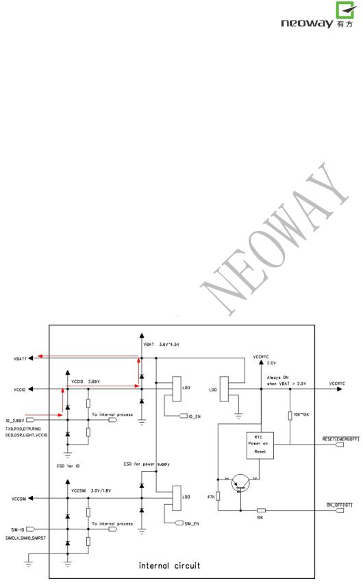
Each digital IO including serial port SIGNAL/LIGHT, and SIM card signal has integrated ESD over-voltage protection, or an input level clamping circuit. For details see Diagram 1.
Should power be removed during operation, with signals still present on any IO, the ports have internal clamping diodes to VBAT.
Refer the red path in Diagram 1. As a result of the IO clamping diodes there may be 2.3V to 2.8V voltage on VBAT/VCCIO. This situation won’t damage the module, but may lead to the external CPU IO exposed to current overload, and affect the module's normal boot.
Diagram 1 IO current feedback to VBAT or other IO’s
Copyright © Shenzhen Neoway Tech Co,.Ltd |
Page 10 of 29 |