

- •Trademarks
- •Devices Included in this Data Sheet:
- •High-Performance RISC CPU:
- •Peripheral Features:
- •CMOS Technology:
- •Pin Diagrams
- •Device Differences
- •Table of Contents
- •Most Current Data Sheet
- •Errata
- •Customer Notification System
- •1.0 General Description
- •1.1 Applications
- •2.0 PIC16C5X Device Varieties
- •2.1 UV Erasable Devices (EPROM)
- •2.5 Read Only Memory (ROM) Devices
- •3.0 Architectural Overview
- •FIGURE 3-1: PIC16C5X Series Block Diagram
- •3.1 Clocking Scheme/Instruction Cycle
- •3.2 Instruction Flow/Pipelining
- •4.0 Oscillator Configurations
- •4.1 Oscillator Types
- •4.2 Crystal Oscillator/Ceramic Resonators
- •FIGURE 4-1: Crystal/Ceramic Resonator Operation (HS, XT or LP OSC Configuration)
- •FIGURE 4-2: External Clock Input Operation (HS, XT or LP OSC Configuration)
- •TABLE 4-1: Capacitor Selection For Ceramic Resonators - PIC16C5X, PIC16CR5X
- •TABLE 4-2: Capacitor Selection For Crystal Oscillator - PIC16C5X, PIC16CR5X
- •4.3 External Crystal Oscillator Circuit
- •4.4 RC Oscillator
- •FIGURE 4-5: RC Oscillator Mode
- •5.0 Reset
- •TABLE 5-1: Status Bits and Their Significance
- •TABLE 5-2: Summary of REgisters Associated with RESET
- •FIGURE 5-1: Simplified Block Diagram of On-Chip Reset Circuit
- •FIGURE 5-2: External Power-On Reset Circuit (For Slow Vdd Power-Up)
- •FIGURE 5-3: Time-Out Sequence on Power-Up (MCLR Not Tied to Vdd)
- •FIGURE 5-4: Time-Out Sequence on Power-Up (MCLR Tied to Vdd): Fast Vdd Rise Time
- •FIGURE 5-5: Time-Out Sequence on Power-Up (MCLR Tied to Vdd): Slow Vdd Rise Time
- •5.2 Device Reset Timer (DRT)
- •FIGURE 5-6: External Brown-Out Protection Circuit 1
- •FIGURE 5-7: External Brown-Out Protection Circuit 2
- •FIGURE 5-8: EXTERNAL BROWN-OUT PROTECTION CIRCUIT 3
- •6.0 Memory Organization
- •6.1 Program Memory Organization
- •FIGURE 6-1: PIC16C54/CR54/C55 Program Memory Map and Stack
- •FIGURE 6-3: PIC16C57/CR57/C58/ CR58 Program Memory Map and Stack
- •6.2 Data Memory Organization
- •FIGURE 6-5: PIC16C57/CR57 Register File Map
- •FIGURE 6-6: PIC16C58/CR58 Register File Map
- •6.3 STATUS Register
- •6.4 OPTION Register
- •6.5 Program Counter
- •6.6 Stack
- •6.7 Indirect Data Addressing; INDF and FSR Registers
- •FIGURE 6-10: Direct/Indirect Addressing
- •7.0 I/O Ports
- •7.1 PORTA
- •7.2 PORTB
- •7.3 PORTC
- •7.4 TRIS Registers
- •7.5 I/O Interfacing
- •FIGURE 7-1: Equivalent Circuit for a Single I/O Pin
- •7.6 I/O Programming Considerations
- •FIGURE 7-2: Successive I/O Operation
- •8.0 Timer0 Module and TMR0 Register
- •FIGURE 8-2: Electrical Structure of T0CKI Pin
- •8.1 Using Timer0 with an External Clock
- •FIGURE 8-5: Timer0 Timing With External Clock
- •8.2 Prescaler
- •FIGURE 8-6: Block Diagram of the Timer0/WDT Prescaler
- •9.0 Special Features of the CPU
- •9.1 Configuration Bits
- •9.2 Watchdog Timer (WDT)
- •9.4 Program Verification/Code Protection
- •9.5 ID Locations
- •10.0 Instruction Set Summary
- •FIGURE 10-1: General Format for Instructions
- •11.0 Development Support
- •11.1 MPLAB Integrated Development Environment Software
- •11.2 MPASM Assembler
- •11.3 MPLAB C17 and MPLAB C18 C Compilers
- •11.4 MPLINK Object Linker/ MPLIB Object Librarian
- •11.5 MPLAB SIM Software Simulator
- •11.9 PRO MATE II Universal Device Programmer
- •11.10 PICSTART Plus Entry Level Development Programmer
- •11.11 PICDEM 1 Low Cost PICmicro Demonstration Board
- •11.12 PICDEM 2 Low Cost PIC16CXX Demonstration Board
- •11.13 PICDEM 3 Low Cost PIC16CXXX Demonstration Board
- •11.14 PICDEM 17 Demonstration Board
- •12.0 Electrical Characteristics - PIC16C54/55/56/57
- •12.6 Timing Parameter Symbology and Load Conditions
- •12.7 Timing Diagrams and Specifications
- •FIGURE 12-2: External Clock Timing - PIC16C54/55/56/57
- •TABLE 12-1: EXTERNAL CLOCK TIMING REQUIREMENTS - PIC16C54/55/56/57
- •FIGURE 12-4: Reset, Watchdog Timer, and Device Reset Timer Timing - PIC16C54/55/56/57
- •TABLE 12-3: Reset, Watchdog Timer, and Device Reset Timer - PIC16C54/55/56/57
- •FIGURE 12-5: Timer0 Clock Timings - PIC16C54/55/56/57
- •TABLE 12-4: Timer0 Clock Requirements - PIC16C54/55/56/57
- •13.0 Electrical Characteristics - PIC16CR54A
- •13.5 Timing Parameter Symbology and Load Conditions
- •FIGURE 13-1: Load Conditions For Device Timing Specifications - PIC16CR54A
- •13.6 Timing Diagrams and Specifications
- •FIGURE 13-2: External Clock Timing - PIC16CR54A
- •TABLE 13-1: External Clock Timing Requirements - PIC16CR54A
- •FIGURE 13-3: CLKOUT and I/O Timing - PIC16CR54A
- •TABLE 13-2: CLKOUT and I/O Timing Requirements - PIC16CR54A
- •FIGURE 13-4: Reset, Watchdog Timer, and Device Reset Timer Timing - PIC16CR54A
- •TABLE 13-3: Reset, Watchdog Timer, and Device Reset Timer - PIC16CR54A
- •FIGURE 13-5: Timer0 Clock Timings - PIC16CR54A
- •14.0 Device Characterization - PIC16C54/55/56/57/CR54A
- •FIGURE 14-1: Typical RC Oscillator Frequency vs. Temperature
- •FIGURE 14-5: Typical Ipd vs. Vdd, Watchdog Disabled
- •FIGURE 14-6: Maximum Ipd vs. Vdd, Watchdog Disabled
- •FIGURE 14-7: Typical Ipd vs. Vdd, Watchdog Enabled
- •FIGURE 14-8: Maximum Ipd vs. Vdd, Watchdog Enabled
- •FIGURE 14-9: Vth (Input Threshold Voltage) of I/O Pins vs. Vdd
- •FIGURE 14-10: Vih, Vil of MCLR, T0CKI and OSC1 (RC Mode) vs. Vdd
- •FIGURE 14-11: Vth (Input Threshold Voltage) of OSC1 Input (XT, HS, and LP modes) vs. Vdd
- •FIGURE 14-12: Typical Idd vs. Frequency (External Clock, 25°C)
- •FIGURE 14-15: WDT Timer Time-out Period vs. Vdd(1)
- •FIGURE 14-16: Transconductance (gm) of HS Oscillator vs. Vdd
- •FIGURE 14-17: Transconductance (gm) of LP Oscillator vs. Vdd
- •FIGURE 14-18: Transconductance (gm) of XT Oscillator vs. Vdd
- •15.0 Electrical Characteristics - PIC16C54A
- •15.5 Timing Parameter Symbology and Load Conditions
- •15.6 Timing Diagrams and Specifications
- •Figure 15-2: External Clock Timing - PIC16C54A
- •TABLE 15-1: External Clock Timing Requirements - PIC16C54A
- •FIGURE 15-4: Reset, Watchdog Timer, and Device Reset Timer Timing - PIC16C54A
- •TABLE 15-3: Reset, Watchdog Timer, and Device Reset Timer - PIC16C54A
- •FIGURE 15-5: Timer0 Clock Timings - PIC16C54A
- •16.0 Device Characterization - PIC16C54A
- •FIGURE 16-1: Typical RC Oscillator Frequency vs. Temperature
- •FIGURE 16-7: Vth (Input Threshold Voltage) of I/O Pins - Vdd
- •FIGURE 16-9: Vih, Vil of MCLR, T0CKI and OSC1 (in RC Mode) vs. Vdd
- •FIGURE 16-10: Typical Idd vs. Frequency (WDT disabled, RC Mode @ 20 pF, 25°C)
- •FIGURE 16-12: Typical Idd vs. Frequency (WDT Disabled, RC Mode @ 100 pF, 25°C)
- •FIGURE 16-14: Typical Idd vs. Frequency (WDT Disabled, RC Mode @ 300 pF, 25°C)
- •FIGURE 16-16: WDT Timer Time-out Period vs. Vdd(1)
- •FIGURE 16-17: Transconductance (gm) of HS Oscillator vs. Vdd
- •FIGURE 16-18: Transconductance (gm) of LP Oscillator vs. Vdd
- •FIGURE 16-19: Transconductance (gm) of XT Oscillator vs. Vdd
- •17.0 Electrical Characteristics - PIC16C54C/CR54C/C55A/C56A/CR56A/ C57C/CR57C/C58B/CR58B
- •17.4 Timing Parameter Symbology and Load Conditions
- •17.5 Timing Diagrams and Specifications
- •FIGURE 17-6: External Clock Timing - PIC16C5X, PIC16CR5X
- •FIGURE 17-8: Reset, Watchdog Timer, and Device Reset Timer Timing - PIC16C5X, PIC16CR5X
- •TABLE 17-3: Reset, Watchdog Timer, and Device Reset Timer - PIC16C5X, PIC16CR5X
- •FIGURE 17-9: Timer0 Clock Timings - PIC16C5X, PIC16CR5X
- •TABLE 17-4: Timer0 Clock Requirements - PIC16C5X, PIC16CR5X
- •FIGURE 18-1: Typical RC Oscillator Frequency vs. Temperature
- •FIGURE 18-5: Typical Ipd vs. Vdd, Watchdog Disabled (25°C)
- •FIGURE 18-6: Typical Ipd vs. Vdd, Watchdog Enabled (25°C)
- •FIGURE 18-8: Vth (Input Threshold Trip Point Voltage) of I/O Pins vs. Vdd
- •FIGURE 18-9: Vih, Vil of MCLR, T0CKI and OSC1 (in RC Mode) vs. Vdd
- •FIGURE 18-11: Typical Idd vs. Frequency (WDT disabled, RC Mode @ 20 pF, 25°C)
- •FIGURE 18-12: Typical Idd vs. Frequency (WDT Disabled, RC Mode @ 100 pF, 25°C)
- •FIGURE 18-13: Typical Idd vs. Frequency (WDT Disabled, RC Mode @ 300 pF, 25°C)
- •FIGURE 18-14: WDT Timer Time-out Period vs. Vdd(1)
- •TABLE 18-2: Input Capacitance
- •19.0 Electrical Characteristics - PIC16C54C/C55A/C56A/C57C/C58B 40MHz
- •19.3 Timing Parameter Symbology and Load Conditions
- •FIGURE 19-2: Load Conditions For Device Timing Specifications - PIC16C54C/C55A/C56A/C57C/C58B-40
- •19.4 Timing Diagrams and Specifications
- •TABLE 19-2: CLKOUT and I/O Timing Requirements - PIC16C5X-40
- •FIGURE 19-5: Reset, Watchdog Timer, and Device Reset Timer Timing - PIC16C5X-40
- •TABLE 19-3: Reset, Watchdog Timer, and Device Reset Timer - PIC16C5X-40
- •FIGURE 19-6: Timer0 Clock Timings - PIC16C5X-40
- •TABLE 19-4: Timer0 Clock Requirements PIC16C5X-40
- •FIGURE 20-1: Typical Ipd vs. Vdd, Watchdog Disabled (25°C)
- •FIGURE 20-2: Typical Ipd vs. Vdd, Watchdog Enabled (25°C)
- •FIGURE 20-4: Vth (Input Threshold Trip Point Voltage) of I/O Pins vs. Vdd
- •FIGURE 20-5: Vth (Input Threshold Trip Point Voltage) of OSC1 Input (HS mode) vs. Vdd
- •FIGURE 20-6: Typical Idd vs. Vdd (40 MHz, WDT disabled, HS Mode, 70°C)
- •FIGURE 20-7: WDT Timer Time-out Period vs. Vdd(1)
- •TABLE 20-1: Input Capacitance
- •FIGURE 20-8: Ioh vs. Voh, Vdd = 5 V
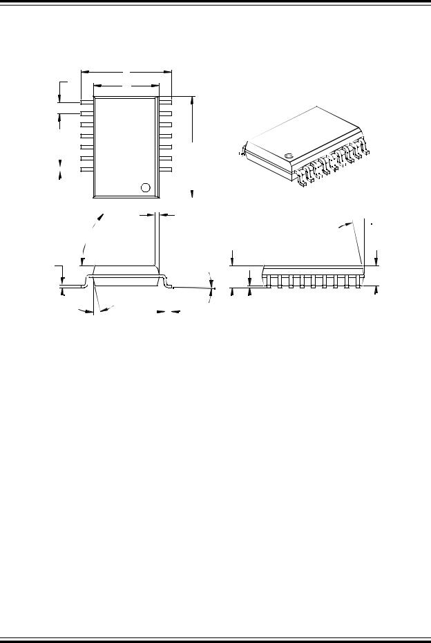
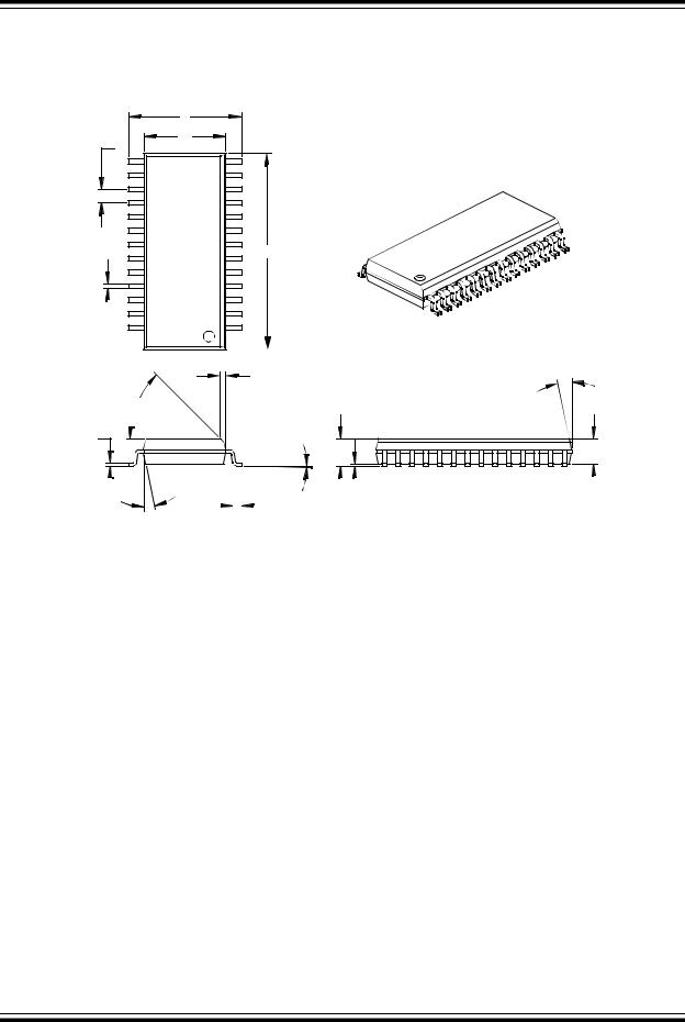
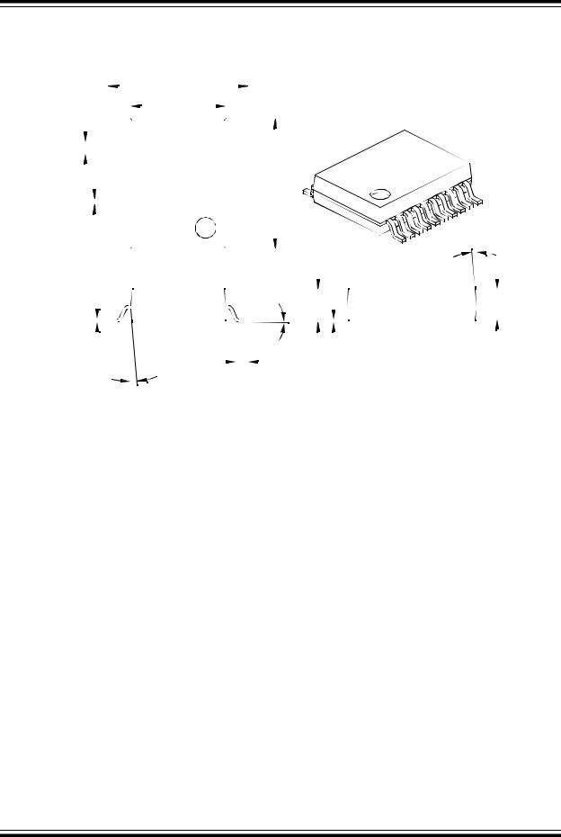
- •21.0 Packaging Information
- •21.1 Package Marketing Information
- •Package Marking Information (Cont’d)
- •On-Line Support
- •Connecting to the Microchip Internet Web Site
- •Systems Information and Upgrade Hot Line
- •Reader Response
- •Product Identification System

PIC16C5X
21.0PACKAGING INFORMATION
21.1Package Marketing Information
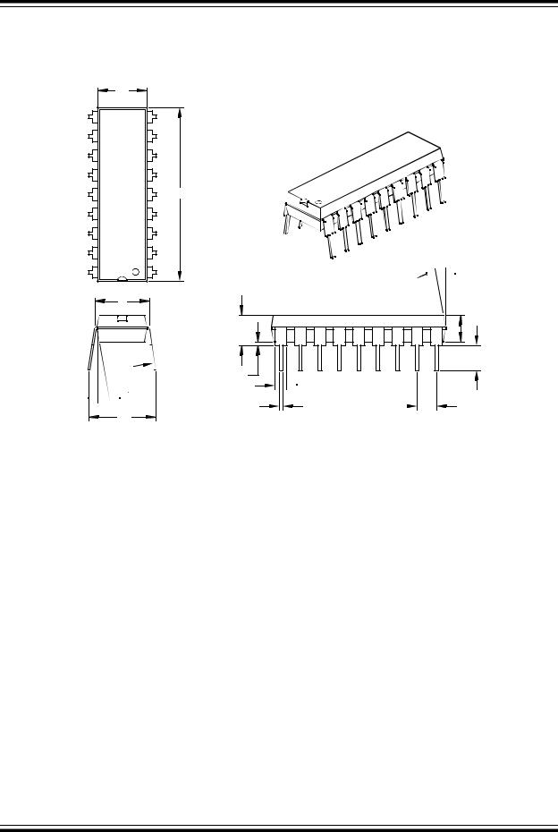
18-Lead PDIP
XXXXXXXXXXXXXXXXX
XXXXXXXXXXXXXXXXX
 YYWWNNN
28-Lead Skinny PDIP (.300")
XXXXXXXXXXXXXXXXX
XXXXXXXXXXXXXXXXX

 YYWWNNN
28-Lead PDIP (.600")
XXXXXXXXXXXXXXX
XXXXXXXXXXXXXXX
XXXXXXXXXXXXXXX
 YYWWNNN
18-Lead SOIC
XXXXXXXXXXXX
XXXXXXXXXXXX
XXXXXXXXXXXX

 YYWWNNN
28-Lead SOIC
XXXXXXXXXXXXXXXXXXXX
XXXXXXXXXXXXXXXXXXXX
XXXXXXXXXXXXXXXXXXXX

 YYWWNNN
20-Lead SSOP
XXXXXXXXXXX
XXXXXXXXXXX

 YYWWNNN
28-Lead SSOP
XXXXXXXXXXXX
XXXXXXXXXXXX

 YYWWNNN
Example
PIC16C56A -04I/P456

 0023CBA
Example
PIC16C55A -04I/SP456

 0023CBA
Example
PIC16C55A -04/P126
 0042CDA
Example
PIC16C54C -04/S0218

 0018CDK
Example
PIC16C57C -04/SO

 0015CBK
Example
PIC16C54C -04/SS218
 0020CBP
Example
PIC16C57C -04/SS123

 0025CBK
ã 2002 Microchip Technology Inc. |
Preliminary |
DS30453D-page 171
PIC16C5X
Package Marking Information (Cont’d)
18-Lead CERDIP Windowed |
Example |
XXXXXXXX
XXXXXXXX
YYWWNNN
28-Lead CERDIP Windowed
PIC16C54C
/JW
0001CBA
Example
XXXXXXXXXXX |
PIC16C57C |
XXXXXXXXXXX |
/JW |
XXXXXXXXXXX |
0038CBA |
YYWWNNN |
Legend: XX...X Customer specific information*
Y Year code (last digit of calendar year)
YY Year code (last 2 digits of calendar year)
WW Week code (week of January 1 is week ‘01’)
NNN Alphanumeric traceability code
Note: In the event the full Microchip part number cannot be marked on one line, it will be carried over to the next line thus limiting the number of available characters for customer specific information.
*Standard PICmicro device marking consists of Microchip part number, year code, week code, and traceability code. For PICmicro device marking beyond this, certain price adders apply. Please check with your Microchip Sales Office. For QTP devices, any special marking adders are included in QTP price.
DS30453D-page 172 |
Preliminary |
ã 2002 Microchip Technology Inc. |
PIC16C5X
18-Lead Plastic Dual In-line (P) – 300 mil (PDIP)
|
E1 |
|
D |
|
2 |
n |
1 |
|
E |

 c
c

 β
β 

eB

 α
α 

 A2
A2
A |
L
A1
 B1
B1
B |
|
p |
|
|
|
Units |
|
INCHES* |
|
MILLIMETERS |
|
||
Dimension Limits |
MIN |
NOM |
MAX |
MIN |
NOM |
|
MAX |
||
Number of Pins |
|
n |
|
18 |
|
|
18 |
|
|
Pitch |
|
p |
|
.100 |
|
|
2.54 |
|
|
Top to Seating Plane |
|
A |
.140 |
.155 |
.170 |
3.56 |
3.94 |
|
4.32 |
Molded Package Thickness |
|
A2 |
.115 |
.130 |
.145 |
2.92 |
3.30 |
|
3.68 |
Base to Seating Plane |
|
A1 |
.015 |
|
|
0.38 |
|
|
|
Shoulder to Shoulder Width |
|
E |
.300 |
.313 |
.325 |
7.62 |
7.94 |
|
8.26 |
Molded Package Width |
|
E1 |
.240 |
.250 |
.260 |
6.10 |
6.35 |
|
6.60 |
Overall Length |
|
D |
.890 |
.898 |
.905 |
22.61 |
22.80 |
|
22.99 |
Tip to Seating Plane |
|
L |
.125 |
.130 |
.135 |
3.18 |
3.30 |
|
3.43 |
Lead Thickness |
|
c |
.008 |
.012 |
.015 |
0.20 |
0.29 |
|
0.38 |
Upper Lead Width |
|
B1 |
.045 |
.058 |
.070 |
1.14 |
1.46 |
|
1.78 |
Lower Lead Width |
|
B |
.014 |
.018 |
.022 |
0.36 |
0.46 |
|
0.56 |
Overall Row Spacing |
§ |
eB |
.310 |
.370 |
.430 |
7.87 |
9.40 |
|
10.92 |
Mold Draft Angle Top |
|
α |
5 |
10 |
15 |
5 |
10 |
|
15 |
Mold Draft Angle Bottom |
|
β |
5 |
10 |
15 |
5 |
10 |
|
15 |
* Controlling Parameter
§ Significant Characteristic
Notes:
Dimensions D and E1 do not include mold flash or protrusions. Mold flash or protrusions shall not exceed
.010” (0.254mm) per side. JEDEC Equivalent: MS-001 Drawing No. C04-007
ã 2002 Microchip Technology Inc. |
Preliminary |
DS30453D-page 173
PIC16C5X
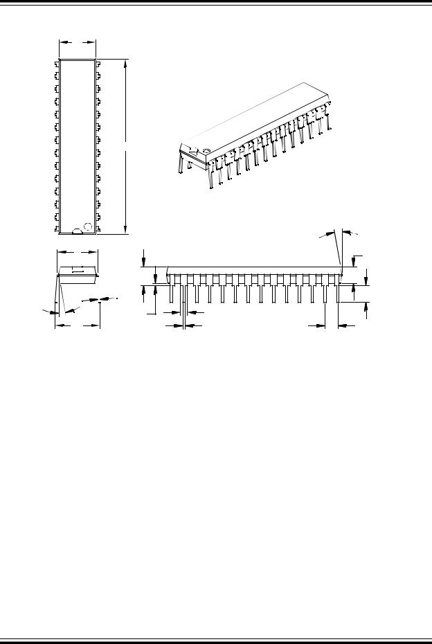
28-Lead Skinny Plastic Dual In-line (SP) – 300 mil (PDIP)
E1 |
|
|
|
|
D |
|
|
|
2 |
|
|
n |
1 |
|
α |
|
|
|
|
E |
|
|
A2 |
|
|
|
|
|
A |
|
|
|
c |
|
L |
|
|
|
|
β |
A1 |
B1 |
|
eB |
|
B |
p |
|
|
Units |
|
INCHES* |
|
MILLIMETERS |
|
|
Dimension Limits |
MIN |
NOM |
MAX |
MIN |
NOM |
MAX |
||
Number of Pins |
|
n |
|
28 |
|
|
28 |
|
Pitch |
|
p |
|
.100 |
|
|
2.54 |
|
Top to Seating Plane |
|
A |
.140 |
.150 |
.160 |
3.56 |
3.81 |
4.06 |
Molded Package Thickness |
|
A2 |
.125 |
.130 |
.135 |
3.18 |
3.30 |
3.43 |
Base to Seating Plane |
|
A1 |
.015 |
|
|
0.38 |
|
|
Shoulder to Shoulder Width |
|
E |
.300 |
.310 |
.325 |
7.62 |
7.87 |
8.26 |
Molded Package Width |
|
E1 |
.275 |
.285 |
.295 |
6.99 |
7.24 |
7.49 |
Overall Length |
|
D |
1.345 |
1.365 |
1.385 |
34.16 |
34.67 |
35.18 |
Tip to Seating Plane |
|
L |
.125 |
.130 |
.135 |
3.18 |
3.30 |
3.43 |
Lead Thickness |
|
c |
.008 |
.012 |
.015 |
0.20 |
0.29 |
0.38 |
Upper Lead Width |
|
B1 |
.040 |
.053 |
.065 |
1.02 |
1.33 |
1.65 |
Lower Lead Width |
|
B |
.016 |
.019 |
.022 |
0.41 |
0.48 |
0.56 |
Overall Row Spacing |
§ |
eB |
.320 |
.350 |
.430 |
8.13 |
8.89 |
10.92 |
Mold Draft Angle Top |
|
α |
5 |
10 |
15 |
5 |
10 |
15 |
Mold Draft Angle Bottom |
|
β |
5 |
10 |
15 |
5 |
10 |
15 |
* Controlling Parameter
§ Significant Characteristic Notes:
Dimension D and E1 do not include mold flash or protrusions. Mold flash or protrusions shall not exceed
.010” (0.254mm) per side. JEDEC Equivalent: MO-095
Drawing No. C04-070
DS30453D-page 174 |
Preliminary |
ã 2002 Microchip Technology Inc. |
PIC16C5X
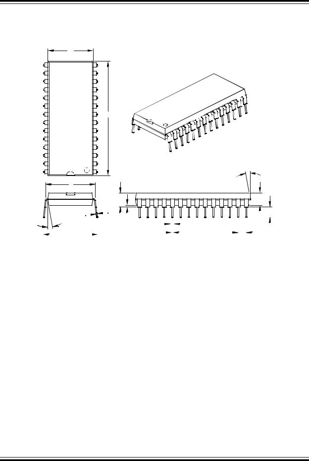
28-Lead Plastic Dual In-line (P) – 600 mil (PDIP)
|
E1 |
|
|
D |
|
|
2 |
|
n |
1 |
α |
|
E |
|
|
A |
A2 |
|
|
β |
|
|
c |
|
|
|
|
|
|
|
|
|
|
|
|
|
B1 |
|
|
|
|
|
|
|
|
|
|
L |
|||||
|
|
|
|
|
|
|
|
|
|
|
|
|
|
|
|
|
|
|
|
|
|
|
|
|
|
||||||||||
|
|
|
|
|
|
|
|
|
|
|
|
|
|
|
|
|
|
|
|
|
|
|
|
|
|
|
|
|
|
|
|
||||
|
|
|
|
A1 |
|
|
|
|
|
|
|
|
|
|
|
|
|
|
|
|
p |
|
|
|
|
|
|
|
|
|
|||||
|
|
|
|
|
|
|
|
|
|
|
|
|
|
|
B |
|
|
|
|
|
|
|
|
|
|
|
|
|
|||||||
|
|
|
eB |
|
|
|
|
|
|
|
|
|
|
|
|
|
|
|
|
|
|
|
|
|
|
|
|
|
|
|
|
||||
|
|
|
|
|
|
|
|
|
|
|
|
|
|
|
|
|
|
|
|
|
|
|
|
|
|
|
|
|
|
|
|||||
|
|
|
|
|
|
|
|
|
|
|
|
|
|
|
|
|
|
|
|
|
|
|
|
|
|
|
|
|
|
|
|
|
|
|
|
|
|
|
|
|
|
|
|
|
|
|
|
|
|
|
|
|
|
|
|
|
|
|
|
|
|
|
|
|
|
|
|
|
|
|
|
|
|
|
|
|
|
|
Units |
|
|
|
INCHES* |
|
|
|
|
|
MILLIMETERS |
|
|
|
|
|
|||||||||||||
|
|
|
|
Dimension Limits |
|
|
MIN |
NOM |
|
|
MAX |
MIN |
|
|
NOM |
|
MAX |
||||||||||||||||||
Number of Pins |
|
|
n |
|
|
|
28 |
|
|
|
|
|
|
28 |
|
|
|
|
|
|
|
||||||||||||||
Pitch |
|
|
p |
|
|
|
.100 |
|
|
|
|
|
|
2.54 |
|
|
|
|
|
|
|
||||||||||||||
Top to Seating Plane |
|
|
A |
|
|
.160 |
.175 |
.190 |
4.06 |
4.45 |
|
|
4.83 |
||||||||||||||||||||||
Molded Package Thickness |
|
|
A2 |
|
|
.140 |
.150 |
.160 |
3.56 |
3.81 |
|
|
4.06 |
||||||||||||||||||||||
Base to Seating Plane |
|
|
A1 |
|
|
.015 |
|
|
|
|
|
|
|
|
|
|
|
0.38 |
|
|
|
|
|
|
|
|
|
|
|
|
|
||||
Shoulder to Shoulder Width |
|
|
E |
|
|
.595 |
.600 |
.625 |
15.11 |
15.24 |
|
|
15.88 |
||||||||||||||||||||||
Molded Package Width |
|
|
E1 |
|
|
.505 |
.545 |
.560 |
12.83 |
13.84 |
|
|
14.22 |
||||||||||||||||||||||
Overall Length |
|
|
D |
|
|
1.395 |
1.430 |
1.465 |
35.43 |
36.32 |
|
|
37.21 |
||||||||||||||||||||||
Tip to Seating Plane |
|
|
L |
|
|
.120 |
.130 |
.135 |
3.05 |
3.30 |
|
|
3.43 |
||||||||||||||||||||||
Lead Thickness |
|
|
c |
|
|
.008 |
.012 |
.015 |
0.20 |
0.29 |
|
|
0.38 |
||||||||||||||||||||||
Upper Lead Width |
|
|
B1 |
|
|
.030 |
.050 |
.070 |
0.76 |
1.27 |
|
|
1.78 |
||||||||||||||||||||||
Lower Lead Width |
|
|
B |
|
|
.014 |
.018 |
.022 |
0.36 |
0.46 |
|
|
0.56 |
||||||||||||||||||||||
Overall Row Spacing |
§ |
|
eB |
|
|
.620 |
.650 |
.680 |
15.75 |
16.51 |
|
|
17.27 |
||||||||||||||||||||||
Mold Draft Angle Top |
|
|
α |
|
|
5 |
10 |
15 |
5 |
10 |
|
|
15 |
||||||||||||||||||||||
Mold Draft Angle Bottom |
|
|
β |
|
|
5 |
10 |
15 |
5 |
10 |
|
|
15 |
||||||||||||||||||||||
* Controlling Parameter
§ Significant Characteristic Notes:
Dimensions D and E1 do not include mold flash or protrusions. Mold flash or protrusions shall not exceed
.010” (0.254mm) per side. JEDEC Equivalent: MO-011 Drawing No. C04-079
ã 2002 Microchip Technology Inc. |
Preliminary |
DS30453D-page 175
PIC16C5X
18-Lead Plastic Small Outline (SO) – Wide, 300 mil (SOIC)
E
p
E1
D
B |
|
|
|
|
|
|
|
|
2 |
|
|
|
|
|
|
|
|
|
|
||
|
|
|
|
|
|
|
|
|
||
|
|
|
|
|
|
|
|
|
||
|
|
|
|
|
|
|
|
|||
|
|
|
|
|
|
|
|
|||
|
|
n |
|
|
|
|
1 |
|
||
|
|
|
|
|
|
|
||||
|
|
|
|
|
|
|
|
|
|
|
h
α 

45°
c
A |
A2 |
|
β |
|
|
|
|
|
|
|
L |
φ |
|
|
|
|
|
|
|
|
|
|
|
|
|
|
|
|
|
|
|
|
|
|
|
|
|
||||
|
|
|
|
|
|
|
|
|
|
|
|
|
|
|
|||||
|
|
|
|
|
|
|
|
|
|
A1 |
|
|
|
|
|
|
|
||
|
|
|
|
|
|
|
|
|
|
|
|
|
|
|
|
||||
|
|
|
|
|
|
|
|
|
|
|
|
|
|
|
|
|
|
||
|
|
|
Units |
|
|
|
|
INCHES* |
|
MILLIMETERS |
|
|
|||||||
|
Dimension Limits |
|
|
MIN |
NOM |
|
MAX |
MIN |
NOM |
|
MAX |
||||||||
Number of Pins |
|
n |
|
|
|
|
18 |
|
|
|
18 |
|
|
|
|||||
Pitch |
|
p |
|
|
|
|
.050 |
|
|
|
1.27 |
|
|
|
|||||
Overall Height |
|
A |
.093 |
.099 |
|
.104 |
2.36 |
2.50 |
|
2.64 |
|||||||||
Molded Package Thickness |
|
A2 |
.088 |
.091 |
|
.094 |
2.24 |
2.31 |
|
2.39 |
|||||||||
Standoff § |
|
A1 |
.004 |
.008 |
|
.012 |
0.10 |
0.20 |
|
0.30 |
|||||||||
Overall Width |
|
E |
.394 |
.407 |
|
.420 |
10.01 |
10.34 |
|
10.67 |
|||||||||
Molded Package Width |
|
E1 |
.291 |
.295 |
|
.299 |
7.39 |
7.49 |
|
7.59 |
|||||||||
Overall Length |
|
D |
.446 |
.454 |
|
.462 |
11.33 |
11.53 |
|
11.73 |
|||||||||
Chamfer Distance |
|
h |
.010 |
.020 |
|
.029 |
0.25 |
0.50 |
|
0.74 |
|||||||||
Foot Length |
|
L |
.016 |
.033 |
|
.050 |
0.41 |
0.84 |
|
1.27 |
|||||||||
Foot Angle |
|
φ |
0 |
4 |
|
8 |
0 |
4 |
|
8 |
|||||||||
Lead Thickness |
|
c |
.009 |
.011 |
|
.012 |
0.23 |
0.27 |
|
0.30 |
|||||||||
Lead Width |
|
B |
.014 |
.017 |
|
.020 |
0.36 |
0.42 |
|
0.51 |
|||||||||
Mold Draft Angle Top |
|
α |
0 |
12 |
|
15 |
0 |
12 |
|
15 |
|||||||||
Mold Draft Angle Bottom |
|
β |
0 |
12 |
|
15 |
0 |
12 |
|
15 |
|||||||||
* Controlling Parameter
§ Significant Characteristic
Notes:
Dimensions D and E1 do not include mold flash or protrusions. Mold flash or protrusions shall not exceed
.010” (0.254mm) per side. JEDEC Equivalent: MS-013 Drawing No. C04-051
DS30453D-page 176 |
Preliminary |
ã 2002 Microchip Technology Inc. |
PIC16C5X
28-Lead Plastic Small Outline (SO) – Wide, 300 mil (SOIC)
E
E1
p
D
B 
2
n |
|
|
|
|
1 |
|
|
|
h |
α |
|
45°
c
A |
A2 |
|
β |
|
|
|
|
|
φ |
|
|
|
|
|
|
|
|
|
|
|
|
|
|
|
|
|
|
|
|
|
|
|
|
||
|
|
|
|
|
|
|
|
|
|
|
|
|
|
|
||
|
|
|
|
|
|
L |
A1 |
|
|
|
|
|
|
|
|
|
|
|
|
|
|
|
|
|
|
|
|
||||||
|
|
|
|
|
|
|
|
|
|
|
|
|
|
|
|
|
|
|
|
|
Units |
|
INCHES* |
|
MILLIMETERS |
|
|
||||||
|
Dimension Limits |
MIN |
|
NOM |
MAX |
MIN |
NOM |
|
MAX |
|||||||
Number of Pins |
|
n |
|
28 |
|
|
28 |
|
|
|
||||||
Pitch |
|
p |
|
.050 |
|
|
1.27 |
|
|
|
||||||
Overall Height |
|
A |
.093 |
.099 |
.104 |
2.36 |
2.50 |
|
2.64 |
|||||||
Molded Package Thickness |
|
A2 |
.088 |
.091 |
.094 |
2.24 |
2.31 |
|
2.39 |
|||||||
Standoff § |
|
A1 |
.004 |
.008 |
.012 |
0.10 |
0.20 |
|
0.30 |
|||||||
Overall Width |
|
E |
.394 |
.407 |
.420 |
10.01 |
10.34 |
|
10.67 |
|||||||
Molded Package Width |
|
E1 |
.288 |
.295 |
.299 |
7.32 |
7.49 |
|
7.59 |
|||||||
Overall Length |
|
D |
.695 |
.704 |
.712 |
17.65 |
17.87 |
|
18.08 |
|||||||
Chamfer Distance |
|
h |
.010 |
.020 |
.029 |
0.25 |
0.50 |
|
0.74 |
|||||||
Foot Length |
|
L |
.016 |
.033 |
.050 |
0.41 |
0.84 |
|
1.27 |
|||||||
Foot Angle Top |
|
φ |
0 |
4 |
8 |
0 |
4 |
|
8 |
|||||||
Lead Thickness |
|
c |
.009 |
.011 |
.013 |
0.23 |
0.28 |
|
0.33 |
|||||||
Lead Width |
|
B |
.014 |
.017 |
.020 |
0.36 |
0.42 |
|
0.51 |
|||||||
Mold Draft Angle Top |
|
α |
0 |
12 |
15 |
0 |
12 |
|
15 |
|||||||
Mold Draft Angle Bottom |
|
β |
0 |
12 |
15 |
0 |
12 |
|
15 |
|||||||
* Controlling Parameter
§ Significant Characteristic
Notes:
Dimensions D and E1 do not include mold flash or protrusions. Mold flash or protrusions shall not exceed
.010” (0.254mm) per side. JEDEC Equivalent: MS-013 Drawing No. C04-052
ã 2002 Microchip Technology Inc. |
Preliminary |
DS30453D-page 177
PIC16C5X
20-Lead Plastic Shrink Small Outline (SS) – 209 mil, 5.30 mm (SSOP)
|
|
|
|
|
|
|
|
|
|
|
|
|
|
|
E |
|
|
|
|
|
|
|
|
|
|
|
|
|
|
|
|
|
|
|
|
|
|
|
|
|
|
|
|
|
|
|
|
|
|
|
|
|
|
|
|
|
|
|
|
|
|
|
|
|
|
|
|
|
|
|
|
|
|
|
|
|
|
|
|
|
|
|
|
|
|
|
|
|
|
|
|
|
|
|
|
|
|
|
|
|
|
|
|
|
|
|
|
|
|
|
|
|
|
|
|
|
|
|
|
|
|
|
|
|
|
||
|
|
|
|
|
|
|
p |
|
|
|
|
|
E1 |
|
|
|
|
|
|
|
|
|
|
|
|
|
|
|
|
|
|
|
|
|
|
|
|
|
|
|
|
|
|
|
|
|
|
|
|
|
|
|
|
|
|
|
|
|
|
||||
|
|
|
|
|
|
|
|
|
|
|
|
|
|
|
|
|
|
|
|
|
|
|
|
|
|
|
|
|
|
|
|
|
|
|
|
|
|
|
|
|
|
|
|
|
|
|
|
|
|
|
|
|
|
|
|
|
|||||||
|
|
|
|
|
|
|
|
|
|
|
|
|
|
|
|
|
|
|
|
|
|
|
|
|
|
|
|
|
|
|
|
|
|
|
|
|
|
|
|
|
|
|
|
|
|
|
|
|
|
|
|
|
|
|
|
|
|
|
|
|
|
||
|
|
|
|
|
|
|
|
|
|
|
|
|
|
|
|
|
|
|
|
|
|
|
|
|
|
|
|
|
|
|
|
|
|
|
|
|
|
|
|
|
|
|
|
|
|
|
|
|
|
|
|
|
|
|
|
|
|
|
|
|
|
|
|
|
|
|
|
|
|
|
|
|
|
|
|
|
|
|
|
|
|
|
|
|
|
|
|
|
|
|
|
|
|
|
|
|
|
|
|
|
|
|
|
|
|
|
|
|
|
|
|
|
|
|
|
|
|
|
|
|
|
|
|
|
|
|
|
|
|
|
|
|
|
|
|
|
|
|
|
|
|
|
|
|
|
|
|
|
|
|
|
|
|
|
|
|
|
|
|
|
|
|
|
|
|
|
|
|
|
|
|
|
|
|
|
|
|
|
|
|
|
|
|
|
|
|
|
|
|
|
|
|
|
|
|
|
|
|
|
|
|
|
|
|
|
|
|
|
|
|
|
|
|
|
|
|
|
|
|
|
|
|
|
|
|
|
|
|
|
|
|
|
|
|
|
|
|
|
|
|
|
|
|
|
|
|
|
|
|
|
|
|
|
|
|
|
|
|
|
|
|
|
|
|
|
|
|
|
|
|
|
|
|
|
|
|
|
|
|
|
|
|
|
|
|
|
|
|
|
|
|
|
|
|
|
|
|
|
|
|
|
|
|
|
|
|
|
|
|
|
|
|
|
|
|
|
|
|
|
|
|
|
|
|
|
|
|
|
|
|
|
|
|
|
|
|
|
|
|
|
|
|
|
|
|
|
|
|
|
|
|
|
|
|
|
|
|
|
|
|
|
|
|
|
|
|
|
|
|
|
|
|
|
|
|
|
|
|
|
|
|
|
|
|
|
|
|
|
|
|
|
|
|
|
|
|
|
|
|
|
|
|
|
|
|
|
|
|
|
|
|
|
|
|
|
|
|
|
|
|
|
|
|
|
|
|
|
|
|
|
|
|
|
|
|
|
|
|
|
|
|
|
|
|
|
|
|
|
|
|
|
|
|
|
|
|
|
|
|
|
|
|
|
|
|
|
|
|
|
|
|
|
|
|
|
|
|
|
|
|
|
|
|
|
|
|
|
|
|
|
|
|
|
|
|
|
|
|
|
|
|
|
|
|
|
|
|
|
|
|
|
B |
|
|
|
|
|
|
|
|
|
|
|
|
|
|
|
|
|
|
|
|
|
|
|
2 |
D |
|
|
|
|
|
|
|
|
|
|
|
|
|
|
|
|
|
|
|
|
|
|
|
|
|
|
|
|
|
|
|
|
|
|
|
|||
|
|
|
|
|
|
|
|
|
|
|
|
|
|
|
|
|
|
|
|
|
|
|
|
|
|
|
|
|
|
|
|
|
|
|
|
|
|
|
|
|
|
|
|
|
|
|
|
|
|
|
|
|
|
|
|
|
|
|
|
|
|||
|
|
|
|
|
|
|
|
|
|
|
|
|
|
|
|
|
|
|
|
|
|
|
|
|
|
|
|
|
|
|
|
|
|
|
|
|
|
|
|
|
|
|
|
|
|
|
|
|
|
|
|
|
|
|
|
|
|
|
|
|
|||
|
|
|
|
|
|
|
|
|
|
|
|
|
|
|
|
|
|
|
|
|
|
|
|
|
|
|
|
|
|
|
|
|
|
|
|
|
|
|
|
|
|
|
|
|
|
|
|
|
|
|
|
|
|
|
|
|
|
|
|
||||
|
|
|
|
|
|
|
|
|
|
|
|
|
|
|
|
|
|
|
|
|
|
|
|
|
|
|
|
|
|
|
|
|
|
|
|
|
|
|
|
|
|
|
|
|
|
|
|
|
|
|
|
|
|
|
|
|
|||||||
|
|
|
|
|
|
|
|
|
|
|
|
|
|
|
|
|
|
|
|
|
|
|
|
|
|
|
|
|
|
|
|
|
|
|
|
|
|
|
|
|
|
|
|
|
|
|
|
|
|
|
|
|
|
|
|||||||||
|
|
|
|
|
|
|
|
|
|
|
|
|
|
|
|
|
|
|
|
|
|
|
|
|
|
|
|
|
|
|
|
|
|
|
|
|
|
|
|
|
|
|
|
|
|
|
|
|
|
|
|
|
|
|
|
|
|
||||||
|
|
|
|
|
|
|
n |
|
|
|
|
|
|
|
|
|
|
|
|
|
1 |
|
|
|
|
|
|
|
|
|
|
|
|
|
|
|
|
|
|
|
|
|
|
|
|
|
|
|
|
|
|
|
|
|
|
|
α |
||||||
|
|
|
|
|
|
|
|
|
|
|
|
|
|
|
|
|
|
|
|
|
|
|
|
|
|
|
|
|
|
|
|
|
|
|
|
|
|
|
|
|
|
|
|
|
|
|
|
|
|
|
|
|
|
|
|||||||||
|
|
|
|
|
|
|
|
|
|
|
|
|
|
|
|
|
|
|
|
|
|
|
|
|
|
|
|
|
|
|
|
|
|
|
|
|
|
|
|
|
|
|
|
|
|
|
|
|
|
|
|
|
|
|
|
|
|
|
|
|
|||
|
|
|
|
|
|
|
|
|
|
|
|
|
|
|
|
|
|
|
|
|
|
|
|
|
|
|
|
|
|
|
|
|
|
|
|
|
|
|
|
|
|
|
|
|
|
|
|
|
|
|
|
|
|
|
|
|
|
|
|
|
|||
|
|
|
|
|
|
|
|
|
|
|
|
|
|
|
|
|
|
|
|
|
|
|
|
|
|
|
|
|
|
|
|
|
|
|
|
|
|
|
|
|
|
|
|
|
|
|
|
|
|
|
|
|
|
|
|
|
|
|
|
|
|||
c |
|
|
|
|
|
|
|
|
|
|
|
|
|
|
|
|
|
|
|
|
|
|
|
|
|
|
|
|
|
|
|
|
|
|
|
|
|
|
|
|
|
|
|
|
|
|
|
|
|
|
|
|
|
|
|||||||||
|
|
|
|
|
|
|
|
|
|
|
|
|
|
|
|
|
|
|
|
|
|
|
|
|
|
|
|
|
|
|
|
|
|
|
|
|
|
|
|
|
|
|
|
|
|
|
|
|
|
|
|
|
|
|
|
|
|
|
|
|
|||
|
|
|
|
|
|
|
|
|
|
|
|
|
|
|
|
|
|
|
|
|
|
|
|
|
|
|
|
|
|
|
|
|
|
|
|
|
|
|
|
|
|
|
|
|
|
|
|
|
|
|
|
|
|
|
|
|
|
|
|
|
|||
|
|
|
|
|
|
|
|
|
|
|
|
|
|
|
|
|
|
|
|
|
|
|
|
A |
|
|
|
|
|
|
|
|
|
|
|
|
|
|
|
|
|
|
|
|
|
|
|
|
|
|
A2 |
||||||||||||
|
|
|
|
|
|
|
|
|
|
|
|
|
|
|
|
|
|
|
|
|
|
|
|
|
|
|
|
|
|
|
|
|
|
|
|
|
|
|
|
|
|
|
|
|
|
|
|
|
|
|
|
|
|
|
|
|
|
|
|
|
|
|
|
|
|
|
|
|
|
|
|
|
|
|
|
|
|
|
|
|
|
|
|
|
|
|
|
|
|
|
φ |
|
|
|
|
|
|
|
|
|
|
|
|
|
|
|
|
|
|
|
|
|
|
|
|
|
|
|
|
|
|
|
|
|
|
|
|
|
|
|
|
|
|
|
|
|
|
|
|
|
|
|
|
|
|
|
|
|
|
|
|
|
|
|
|
|
|
|
|
|
|
|
|
|
|
|
|
|
|
|
|
|
|
|
|
|
|
|
|
|
|
|
|
|
|
|
|
|
|
||
|
|
|
|
|
|
|
|
|
|
|
|
|
|
|
|
|
|
|
|
|
|
|
|
|
|
|
|
|
|
|
|
|
|
|
|
|
|
|
|
|
|
|
|
|
|
|
|
|
|
|
|
|
|
|
|
|
|
|
|
|
|
||
|
|
|
|
|
|
|
|
β |
|
|
|
|
|
|
|
|
|
|
|
|
|
|
|
L |
|
A1 |
|
|
|
|
|
|
|
|
|
|
|
|
|
|
|
|
|
|
|
|
|
|
|
|
|
|
|
|
|
|
|||||||
|
|
|
|
|
|
|
|
|
|
|
|
|
|
|
|
|
|
|
|
|
|
|
|
|
|
|
|
|
|
|
|
|
|
|
|
|
|
|
|
|
|
|
|
|
|
|
|
|
|
|
|
|
|||||||||||
|
|
|
|
|
|
|
|
|
|
|
|
|
|
|
|
|
|
|
|
|
|
|
|
|
|
|
|
|
|
|
|
|
|
|
|
|
|
|
|
|
|
|
|
|
|
|
|
|
|
|
|
|
|
|
|
|
|
|
|||||
|
|
|
|
|
|
|
|
|
|
|
|
|
|
|
|
|
|
|
|
|
|
|
|
|
|
|
|
|
|
|
|
|
|
|
|
|
|
|
|
|
|
|
|
|
|
|
|
|
|
|
|
|
|
|
|
|
|
|
|
|
|
||
|
|
|
|
|
|
|
|
|
|
|
|
|
|
|
|
|
|
|
|
|
|
|
|
|
|
|
|
|
|
|
|
|
|
|
|
|
|
|
|
|
|
|
|
|
|
|
|
|
|
|
|
|
|
|
|
|
|
|
|
|
|
|
|
|
|
|
|
|
|
|
|
|
|
|
|
|
|
|
|
|
|
Units |
|
|
|
|
|
|
|
|
INCHES* |
|
|
|
|
|
|
|
|
|
|
|
|
|
|
MILLIMETERS |
|
|
|
||||||||||||||||||
|
|
|
|
|
|
|
|
|
|
|
|
|
Dimension Limits |
|
|
|
MIN |
|
|
NOM |
|
|
|
MAX |
|
|
|
MIN |
|
|
NOM |
|
|
MAX |
|||||||||||||||||||||||||||||
Number of Pins |
|
|
|
|
n |
|
|
|
|
|
|
|
|
20 |
|
|
|
|
|
|
|
|
|
|
|
|
|
|
|
|
|
|
20 |
|
|
|
|
|
|
||||||||||||||||||||||||
Pitch |
|
|
|
|
p |
|
|
|
|
|
|
|
|
.026 |
|
|
|
|
|
|
|
|
|
|
|
|
|
|
|
|
|
|
0.65 |
|
|
|
|
|
|
||||||||||||||||||||||||
Overall Height |
|
|
|
|
A |
.068 |
|
|
.073 |
|
|
|
.078 |
1.73 |
1.85 |
|
|
|
1.98 |
||||||||||||||||||||||||||||||||||||||||||||
Molded Package Thickness |
|
|
|
|
A2 |
.064 |
|
|
.068 |
|
|
|
.072 |
1.63 |
1.73 |
|
|
|
1.83 |
||||||||||||||||||||||||||||||||||||||||||||
Standoff § |
|
|
|
|
A1 |
.002 |
|
|
.006 |
|
|
|
.010 |
0.05 |
0.15 |
|
|
|
0.25 |
||||||||||||||||||||||||||||||||||||||||||||
Overall Width |
|
|
|
|
E |
.299 |
|
|
.309 |
|
|
|
.322 |
7.59 |
7.85 |
|
|
|
8.18 |
||||||||||||||||||||||||||||||||||||||||||||
Molded Package Width |
|
|
|
|
E1 |
.201 |
|
|
.207 |
|
|
|
.212 |
5.11 |
5.25 |
|
|
|
5.38 |
||||||||||||||||||||||||||||||||||||||||||||
Overall Length |
|
|
|
|
D |
.278 |
|
|
.284 |
|
|
|
.289 |
7.06 |
7.20 |
|
|
|
7.34 |
||||||||||||||||||||||||||||||||||||||||||||
Foot Length |
|
|
|
|
L |
.022 |
|
|
.030 |
|
|
|
.037 |
0.56 |
0.75 |
|
|
|
0.94 |
||||||||||||||||||||||||||||||||||||||||||||
Lead Thickness |
|
|
|
|
c |
.004 |
|
|
.007 |
|
|
|
.010 |
0.10 |
0.18 |
|
|
|
0.25 |
||||||||||||||||||||||||||||||||||||||||||||
Foot Angle |
|
|
|
|
φ |
0 |
|
|
4 |
|
|
8 |
0.00 |
101.60 |
|
|
|
203.20 |
|||||||||||||||||||||||||||||||||||||||||||||
Lead Width |
|
|
|
|
B |
.010 |
|
|
.013 |
|
|
|
.015 |
0.25 |
0.32 |
|
|
|
0.38 |
||||||||||||||||||||||||||||||||||||||||||||
Mold Draft Angle Top |
|
|
|
|
α |
0 |
|
|
5 |
|
|
10 |
0 |
5 |
|
|
|
10 |
|||||||||||||||||||||||||||||||||||||||||||||
Mold Draft Angle Bottom |
|
|
|
|
β |
0 |
|
|
5 |
|
|
10 |
0 |
5 |
|
|
|
10 |
|||||||||||||||||||||||||||||||||||||||||||||
* Controlling Parameter
§ Significant Characteristic
Notes:
Dimensions D and E1 do not include mold flash or protrusions. Mold flash or protrusions shall not exceed
.010” (0.254mm) per side. JEDEC Equivalent: MO-150 Drawing No. C04-072
DS30453D-page 178 |
Preliminary |
ã 2002 Microchip Technology Inc. |
PIC16C5X
28-Lead Plastic Shrink Small Outline (SS) – 209 mil, 5.30 mm (SSOP)
E
E1
p
|
|
|
|
|
|
|
|
|
|
|
|
|
|
|
|
|
|
|
|
|
|
|
|
|
|
|
|
|
|
|
|
|
|
|
|
|
|
|
|
|
|
|
|
|
|
|
|
|
|
|
|
|
|
|
|
|
|
|
|
|
|
|
|
|
|
|
|
|
|
|
|
|
|
|
|
|
|
|
|
|
|
|
|
|
|
|
|
|
|
|
|
|
|
|
|
|
|
|
|
|
|
|
|
|
|
|
|
|
|
|
|
|
|
|
|
|
|
|
|
|
|
|
|
|
|
|
|
|
|
|
|
|
|
|
|
|
|
|
|
|
|
|
|
|
|
|
|
|
|
|
|
|
|
|
|
|
|
|
|
|
|
|
|
|
|
|
|
|
|
|
|
|
|
|
|
|
|
|
|
|
|
|
|
|
|
|
|
|
|
|
|
|
|
|
|
|
|
|
|
|
|
|
|
|
|
|
|
|
|
|
|
|
|
|
|
|
|
|
|
|
|
|
|
|
|
|
|
|
|
|
|
|
|
|
|
|
|
|
|
|
|
|
|
|
|
|
|
|
|
|
|
|
|
|
|
|
|
|
|
|
|
|
|
|
|
|
|
B |
|
|
|
|
|
|
|
|
|
|
|
|
|
|
|
|
|
|
2 |
|
D |
|
|
|
|
|
|
|
|
|
|
|
|
|
|
|
|
|
|
|
|
|
|
|
|
|
|
|
|
|
|
|
|
|
|
|
|
|
|
|
|
|
||||
|
|
|
|
|
|
|
|
|
|
|
|
|
|
|
|
|
|
|
|
|
|
|
|
|
|
|
|
|
|
|
|
|
|
|
|
|
|
|
|
|
|
|
|
|
|
|
|
|
|
|
|
|
|
|
|
|
|
|
|
|
|
|
|
|||
|
|
|
|
|
|
|
|
|
|
|
|
|
|
|
|
|
|
|
|
|
|
|
|
|
|
|
|
|
|
|
|
|
|
|
|
|
|
|
|
|
|
|
|
|
|
|
|
|
|
|
|
|
|
|
|
|
|
|
|
|
|
|
|
|||
|
|
|
|
|
|
|
|
|
|
|
|
|
|
|
|
|
|
|
|
|
|
|
|
|
|
|
|
|
|
|
|
|
|
|
|
|
|
|
|
|
|
|
|
|
|
|
|
|
|
|
|
|
|
|
|
|
|
|
|
|
|
|
|
|||
|
|
|
|
|
|
|
|
|
|
|
|
|
|
|
|
|
|
|
|
|
|
|
|
|
|
|
|
|
|
|
|
|
|
|
|
|
|
|
|
|
|
|
|
|
|
|
|
|
|
|
|
|
|
|
|
|
|
|
|
|
||||||
|
|
|
|
|
|
|
|
|
|
|
|
|
|
|
|
|
|
|
|
|
|
|
|
|
|
|
|
|
|
|
|
|
|
|
|
|
|
|
|
|
|
|
|
|
|
|
|
|
|
|
|
|
|
|
|
|
|
|
|
|
|
|
|
|||
|
|
|
|
|
|
|
|
|
|
|
|
|
|
|
|
|
|
|
|
|
|
|
|
|
|
|
|
|
|
|
|
|
|
|
|
|
|
|
|
|
|
|
|
|
|
|
|
|
|
|
|
|
|
|
|
|
|
|
|
|
|
|
|
|||
|
|
|
|
|
|
|
|
|
|
|
|
|
|
|
|
|
|
|
|
|
|
|
|
|
|
|
|
|
|
|
|
|
|
|
|
|
|
|
|
|
|
|
|
|
|
|
|
|
|
|
|
|
|
|
|
|
|
|
|
|
|
|
|
|||
|
|
|
|
n |
|
|
|
|
|
|
|
|
|
|
|
|
|
|
|
|
|
|
|
|
|
|
|
|
|
|
|
|
|
|
|
|
|
|
|
|
|
|
|
|
|
|
|
|
|
|
|
|
|
|
|
|
|
|
|
|
|
|
||||
|
|
|
|
|
|
|
|
|
|
|
|
|
|
|
|
|
|
|
|
|
|
|
|
|
|
|
|
|
|
|
|
|
|
|
|
|
|
|
|
|
|
|
|
|
|
|
|
|
|
|
|
|
|
|
|
|
|
|
|
|
|
|
|
|||
|
|
|
|
|
|
|
|
|
|
|
|
|
|
|
|
|
|
|
|
|
|
|
|
|
|
|
|
|
|
|
|
|
|
|
|
|
|
|
|
|
|
|
|
|
|
|
|
|
|
|
|
|
|
|
|
|
|
|
|
|
|
|
|
|||
|
|
|
|
|
|
|
|
|
|
|
|
|
|
|
|
|
|
1 |
|
|
|
|
|
|
|
|
|
|
|
|
|
|
|
|
|
|
|
|
|
|
|
|
|
|
|
|
|
|
|
|
|
|
|
|
|
|
|
|
|
|
|
|
α |
|||
|
|
|
|
|
|
|
|
|
|
|
|
|
|
|
|
|
|
|
|
|
|
|
|
|
|
|
|
|
|
|
|
|
|
|
|
|
|
|
|
|
|
|
|
|
|
|
|
|
|
|
|
|
|
|||||||||||||
|
|
|
|
|
|
|
|
|
|
|
|
|
|
|
|
|
|
|
|
|
|
|
|
|
|
|
|
|
|
|
|
|
|
|
|
|
|
|
|
|
|
|
|
|
|
|
|
|
|
|
|
|
|
|
|
|
|
|
|
|
|
|
|
|
||
|
|
|
|
|
|
|
|
|
|
|
|
|
|
|
|
|
|
|
|
|
|
|
|
|
|
|
|
|
|
|
|
|
|
|
|
|
|
|
|
|
|
|
|
|
|
|
|
|
|
|
|
|
|
|
|
|
|
|
|
|
|
|
|
|
||
|
|
|
|
|
|
|
|
|
|
|
|
|
|
|
|
|
|
|
|
|
|
|
|
|
|
|
|
|
|
|
|
|
|
|
|
|
|
|
|
|
|
|
|
|
|
|
|
|
|
|
|
|
|
|
|
|
|
|
|
|
|
|
|
|
||
|
|
|
|
|
|
|
|
|
|
|
|
|
|
|
|
|
|
|
|
|
|
|
|
|
|
|
|
|
|
|
|
|
|
|
|
|
|
|
|
|
|
|
|
|
|
|
|
|
|
|
|
|
|
|
|
|
|
|
|
|
|
|
|
|
||
c |
|
|
|
|
|
|
|
|
|
|
|
|
|
|
|
|
|
|
|
|
|
|
|
|
|
|
|
|
A |
|
|
|
|
|
|
|
|
|
|
|
|
|
|
|
|
|
|
|
|
|
|
|
|
|
|
|
|
|
|
|
|
|
||||
|
|
|
|
|
|
|
|
|
|
|
|
|
|
|
|
|
|
|
|
|
|
|
|
|
|
|
|
|
|
|
|
|
|
|
|
|
|
|
|
|
|
|
|
|
|
|
|
|
|
|
|
|
|
|
|
|
|
|
|
|
||||||
|
|
|
|
|
|
|
|
|
|
|
|
|
|
|
|
|
|
|
|
|
|
|
|
|
|
|
|
|
|
|
|
|
|
|
|
|
|
|
|
|
|
|
|
|
|
|
|
|
|
|
|
|
|
|
|
|
||||||||||
|
|
|
|
|
|
|
|
|
|
|
|
|
|
|
|
|
|
|
|
|
|
|
|
|
|
|
|
|
|
|
|
|
|
|
|
|
|
|
|
|
|
|
|
|
|
|
|
|
|
|
|
|
|
|
|
|
|
|
|
|
A2 |
|||||
|
|
|
|
|
|
|
|
|
|
|
|
|
|
|
|
|
|
|
|
|
|
|
|
|
|
|
|
|
|
|
|
|
|
|
|
|
|
|
|
|
|
|
|
|
|
|
|
|
|
|
|
|
|
|
|
|
|
|
|
|
|
|
|
|||
|
|
|
|
|
|
|
|
|
|
|
|
|
|
|
|
|
|
|
|
|
|
|
|
|
|
|
|
|
|
|
|
|
|
|
|
|
|
|
|
|
|
|
|
|
|
|
|
|
|
|
|
|
|
|
|
|
|
|
|
|
|
|
|
|
|
|
|
|
|
|
|
|
|
|
|
|
|
|
|
|
|
|
|
|
|
|
|
|
|
|
|
|
|
|
|
|
|
|
|
|
|
|
|
|
|
|
|
|
|
|
|
|
|
|
|
|
|
|
|
|
|
|
|
|
|
|
|
|
|
|
|
|
|
|
|
|
|
|
|
|
|
|
|
|
|
|
|
|
|
|
|
|
|
|
|
φ |
A1 |
|
|
|
|
|
|
|
|
|
|
|
|
|
|
|
|
|
|
|
|
|
|
|
|
|
|
|
|
|
|
|
|
|
|
|
|
|
|
|
||||
|
|
|
|
|
|
|
|
|
|
|
|
|
|
|
|
|
|
|
|
|
|
|
|
|
|
|
|
|
|
|
|
|
|
|
|
|
|
|
|
|
|
|
|
|
|
|
|
|
|
|
|
|
|
|
|
|
|
|
|
|||||||
|
|
|
|
|
|
|
|
|
|
|
|
|
|
|
|
|
|
|
|
|
|
|
|
|
|
|
|
|
|
|
|
|
|
|
|
|
|
|
|
|
|
|
|
|
|
|
|
|
|
|
|
|
|
|
|
|||||||||||
|
|
|
|
|
|
β |
|
|
|
|
|
|
|
|
|
|
|
L |
|
|
|
|
|
|
|
|
|
|
|
|
|
|
|
|
|
|
|
|
|
|
|
|
|
|
|
|
|
|
|
|
|
|
|
|
|
|
|
|
|
|||||||
|
|
|
|
|
|
|
|
|
|
|
|
|
|
|
|
|
|
|
|
|
|
|
|
|
|
|
|
|
|
|
|
|
|
|
|
|
|
|
|
|
|
|
|
|
|
|
|
|
|
|
|
|
|
|
|
|
||||||||||
|
|
|
|
|
|
|
|
|
|
|
|
|
|
|
|
|
|
|
|
|
|
|
|
|
|
|
|
|
|
|
|
|
|
|
|
|
|
|
|
|
|
|
|
|
|
|
|
|
|
|
|
|
|
|
|
|
|
|
|
|
|
|||||
|
|
|
|
|
|
|
|
|
|
|
|
|
|
|
|
|
|
|
|
|
|
|
|
|
|
|
|
|
|
|
|
|
|
|
|
|
|
|
|
|
|
|
|
|
|
|
|
|
|
|
|
|
|
|
|
|
|
|
|
|
|
|
|
|
|
|
|
|
|
|
|
|
|
|
|
|
|
|
|
|
|
Units |
|
|
|
|
|
|
|
INCHES |
|
|
|
|
|
|
|
|
|
|
|
|
|
|
|
|
|
|
MILLIMETERS* |
|
|
|
|||||||||||||||||||||
|
|
|
|
|
|
|
|
|
|
|
|
|
Dimension Limits |
|
|
MIN |
NOM |
|
|
|
MAX |
|
|
|
MIN |
|
|
NOM |
|
MAX |
||||||||||||||||||||||||||||||||||||
Number of Pins |
|
n |
|
|
|
|
|
|
|
28 |
|
|
|
|
|
|
|
|
|
|
|
|
|
|
|
|
|
|
|
|
28 |
|
|
|
|
|||||||||||||||||||||||||||||||
Pitch |
|
p |
|
|
|
|
|
|
|
.026 |
|
|
|
|
|
|
|
|
|
|
|
|
|
|
|
|
|
|
|
|
0.65 |
|
|
|
|
|||||||||||||||||||||||||||||||
Overall Height |
|
A |
.068 |
.073 |
.078 |
1.73 |
1.85 |
|
1.98 |
|||||||||||||||||||||||||||||||||||||||||||||||||||||||||
Molded Package Thickness |
|
A2 |
.064 |
.068 |
.072 |
1.63 |
1.73 |
|
1.83 |
|||||||||||||||||||||||||||||||||||||||||||||||||||||||||
Standoff § |
|
A1 |
.002 |
.006 |
.010 |
0.05 |
0.15 |
|
0.25 |
|||||||||||||||||||||||||||||||||||||||||||||||||||||||||
Overall Width |
|
E |
.299 |
.309 |
.319 |
7.59 |
7.85 |
|
8.10 |
|||||||||||||||||||||||||||||||||||||||||||||||||||||||||
Molded Package Width |
|
E1 |
.201 |
.207 |
.212 |
5.11 |
5.25 |
|
5.38 |
|||||||||||||||||||||||||||||||||||||||||||||||||||||||||
Overall Length |
|
D |
.396 |
.402 |
.407 |
10.06 |
10.20 |
|
10.34 |
|||||||||||||||||||||||||||||||||||||||||||||||||||||||||
Foot Length |
|
L |
.022 |
.030 |
.037 |
0.56 |
0.75 |
|
0.94 |
|||||||||||||||||||||||||||||||||||||||||||||||||||||||||
Lead Thickness |
|
c |
.004 |
.007 |
.010 |
0.10 |
0.18 |
|
0.25 |
|||||||||||||||||||||||||||||||||||||||||||||||||||||||||
Foot Angle |
|
φ |
0 |
4 |
8 |
0.00 |
101.60 |
|
203.20 |
|||||||||||||||||||||||||||||||||||||||||||||||||||||||||
Lead Width |
|
B |
.010 |
.013 |
.015 |
0.25 |
0.32 |
|
0.38 |
|||||||||||||||||||||||||||||||||||||||||||||||||||||||||
Mold Draft Angle Top |
|
α |
0 |
5 |
10 |
0 |
5 |
|
10 |
|||||||||||||||||||||||||||||||||||||||||||||||||||||||||
Mold Draft Angle Bottom |
|
β |
0 |
5 |
10 |
0 |
5 |
|
10 |
|||||||||||||||||||||||||||||||||||||||||||||||||||||||||
|
|
|
|
|
|
|||||||||||||||||||||||||||||||||||||||||||||||||||||||||||||
* Controlling Parameter
§ Significant Characteristic
Notes:
Dimensions D and E1 do not include mold flash or protrusions. Mold flash or protrusions shall not exceed
.010” (0.254mm) per side. JEDEC Equivalent: MS-150 Drawing No. C04-073
ã 2002 Microchip Technology Inc. |
Preliminary |
DS30453D-page 179
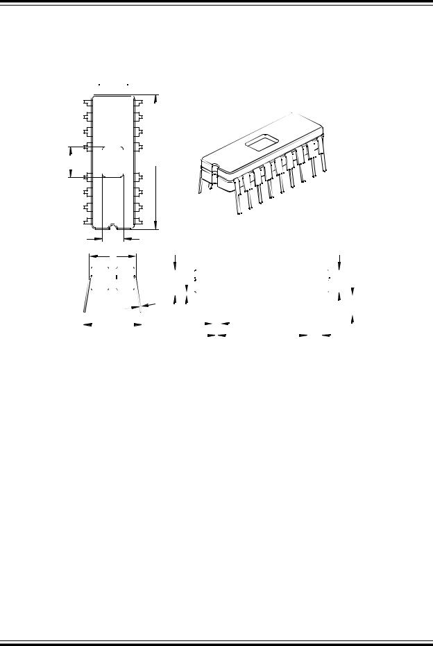
PIC16C5X
18-Lead Ceramic Dual In-line with Window (JW) – 300 mil (CERDIP)
 E1
E1

|
|
|
|
|
|
|
|
|
|
|
|
|
|
|
|
|
|
|
|
|
|
|
|
|
|
|
|
|
|
|
|
|
|
|
|
|
|
|
|
|
|
|
|
|
|
|
|
|
|
|
|
|
|
|
|
|
|
|
|
W2 |
|
|
|
|
|
|
|
|
|
D |
||||
|
|
|
|
|
|
|
|
|
|
|
|
|
|
|
|
|
|
|
|
|
|
|
|
|
|
|
|
|
|
|
2 |
n |
1 |
|
W1 |
|
E |
|
|
|
|
|
|
|
|
|
|
|
|
|
|
|
|
|
|
|
|
|
|
|
|
|
|
|
|
|
|
|
|
|
|
|
|
|
|
|
|
|
|
|
|
|
|
|
|
|
|
|
|
|
|
|
|
|
|
|
|
|
|
|
|
|
|
|
|
|
|
|
|
c |
|
A |
|
|
|
|
|
|
|
|
|
|
|
|
|
|
|
|
|
|
|
|
|
|
|
|
|
|
|
|
|
|
|
|
|
|
|
|
|
|
A2 |
|
|
||||||
|
|
|
|
|
|
|
|
|
|
|
|
|
|
|
|
|
|
|
|
|
|
|
|
|
|
|
|
|
|
|
|
|
|
|
|
|
|
|
|
|
|
|
|
|
|
|
|
|
|
|
|
|
|
|
|
|
|
|
|
|
|
|
|
|
|
|
|
|
|
|
|
|
|
|
|
|
|
|
|
|
|
|
|
|
|
|
|
|
|
|
|
|
|
|
|
|
|
|
|
|
|
|
|
|
|
|
|
|
|
|
|
|
|
|
|
|
|
|
|
||
|
|
|
|
|
|
|
|
|
|
|
|
|
|
|
|
|
|
|
|
|
|
|
|
|
|
|
|
|
|
|
|
|
|
|
|
|
|
|
|
|
|
|
|
|
|
|
|
|
|
|
|
|
|
|
|
|
|
|
||
|
|
|
|
|
|
|
|
|
|
|
|
|
|
|
|
|
|
|
|
|
|
|
|
|
|
|
|
|
|
|
|
|
|
|
|
|
|
|
|
|
|
|
|
|
|
|
|
|
|
|
|
|
|
|
|
|
|
|
|
|
|
|
|
|
|
|
|
|
|
|
|
|
|
|
|
|
|
|
|
|
|
|
|
|
|
|
|
|
|
|
|
|
|
|
|
|
|
|
|
|
|
|
|
|
|
|
|
|
|
|
|
|
|
|
|
|
|
|
|
|
|
|
|
|
|
|
|
|
|
|
|
|
|
|
|
|
|
|
|
|
|
|
|
|
|
|
|
|
|
|
|
|
|
|
|
|
|
|
|
|
|
|
|
|
|
|
|
|
|
|
|
|
|
|
|
|
|
|
L |
|
||
|
|
|
|
|
|
|
|
|
|
|
|
|
|
|
|
|
|
|
|
|
|
|
|
|
|
|
|
|
|
|
|
|
|
|
|
|
|
|
|
|
|
|
|
|
|
|
|
|
|
|
|
|
|
|
|
|
|
|||
|
|
|
|
|
|
|
|
|
|
|
|
|
|
|
|
|
|
|
|
|
|
|
|
|
|
|
|
|
|
|
|
|
|
|
|
|
|
|
|
|
|
|
|
|
|
|
|
|
|
|
|
|
|
|
|
|
|
|||
|
|
|
|
|
|
|
|
|
|
|
|
|
|
|
|
|
|
|
|
|
|
|
|
|
|
|
|
|
|
|
|
|
|
|
|
|
|
|
|
|
|
|
|
|
|
|
|
|
|
|
|
|
|
|
|
|
|
|
|
|
|
|
|
|
|
|
|
|
|
|
|
|
A1 |
|
|
|
|
|
|
|
|
|
|
|
|
|
|
|
|
|
|
|
|
|
|
|
|
|
|
|
|
|
|
|
|
|
|
|
|
|
|
|
|
|
|
|
|
|
|
||
|
|
|
|
eB |
|
|
|
|
|
|
|
|
|
|
|
|
|
|
|
|
|
|
B1 |
|
|
|
|
|
|
|
|
|
|
|
|
|
|
|
|
p |
|
|
|
|
|
|
|
|||||||||||||
|
|
|
|
|
|
|
|
|
|
|
|
|
|
|
|
|
|
|
|
|
|
|
|
|
|
|
|
|
|
|
|
|
|
|
|
|
|
|
|
|
|
|
|
|
||||||||||||||||
|
|
|
|
|
|
|
|
|
|
|
|
|
|
|
|
|
|
|
|
|
|
|
|
|
|
|
|
|
|
|
|
|
|
|
|
|
|
|
|
|
|
|
|
|
|
|
|
|
|
|
|
|||||||||
|
|
|
|
|
|
|
|
|
|
|
|
|
|
|
|
|
|
|
|
|
|
|
|
|
|
|
|
|
|
B |
|
|
|
|
|
|
|
|
|
|
|
|
|
|
|
|
|
|
|
|
|
|
|
|||||||
|
|
|
|
|
|
|
|
|
|
|
|
|
|
|
|
|
|
|
|
|
|
|
|
|
|
|
|
|
|
|
|
|
|
|
|
|
|
|
|
|
|
|
|
|
|
|
|
|
|
|
|
|
|
|
|
|
|
|
|
|
|
|
|
|
|
|
|
|
|
|
|
Units |
|
|
|
|
|
|
|
|
|
|
INCHES* |
|
|
|
|
|
|
|
|
|
|
|
|
|
|
|
|
MILLIMETERS |
|
||||||||||||||||||||
|
|
|
|
Dimension Limits |
|
|
|
MIN |
|
|
|
NOM |
|
|
|
MAX |
|
|
|
MIN |
|
|
NOM |
|
MAX |
|||||||||||||||||||||||||||||||||||
Number of Pins |
|
|
|
|
n |
|
|
|
|
|
|
|
|
|
18 |
|
|
|
|
|
|
|
|
|
|
|
|
|
|
|
|
|
|
|
|
|
|
18 |
|
|
||||||||||||||||||||
Pitch |
|
|
|
|
p |
|
|
|
|
|
|
|
|
|
.100 |
|
|
|
|
|
|
|
|
|
|
|
|
|
|
|
|
|
|
|
|
|
|
2.54 |
|
|
||||||||||||||||||||
Top to Seating Plane |
|
|
|
|
A |
.170 |
.183 |
|
|
|
.195 |
4.32 |
|
|
4.64 |
|
4.95 |
|||||||||||||||||||||||||||||||||||||||||||
Ceramic Package Height |
|
|
|
|
A2 |
.155 |
.160 |
|
|
|
.165 |
3.94 |
|
|
4.06 |
|
4.19 |
|||||||||||||||||||||||||||||||||||||||||||
Standoff |
|
|
|
|
A1 |
.015 |
.023 |
|
|
|
.030 |
0.38 |
|
|
0.57 |
|
0.76 |
|||||||||||||||||||||||||||||||||||||||||||
Shoulder to Shoulder Width |
|
|
|
|
E |
.300 |
.313 |
|
|
|
.325 |
7.62 |
|
|
7.94 |
|
8.26 |
|||||||||||||||||||||||||||||||||||||||||||
Ceramic Pkg. Width |
|
|
|
|
E1 |
.285 |
.290 |
|
|
|
.295 |
7.24 |
|
|
7.37 |
|
7.49 |
|||||||||||||||||||||||||||||||||||||||||||
Overall Length |
|
|
|
|
D |
.880 |
.900 |
|
|
|
.920 |
22.35 |
|
|
22.86 |
|
23.37 |
|||||||||||||||||||||||||||||||||||||||||||
Tip to Seating Plane |
|
|
|
|
L |
.125 |
.138 |
|
|
|
.150 |
3.18 |
|
|
3.49 |
|
3.81 |
|||||||||||||||||||||||||||||||||||||||||||
Lead Thickness |
|
|
|
|
c |
.008 |
.010 |
|
|
|
.012 |
0.20 |
|
|
0.25 |
|
0.30 |
|||||||||||||||||||||||||||||||||||||||||||
Upper Lead Width |
|
|
|
|
B1 |
.050 |
.055 |
|
|
|
.060 |
1.27 |
|
|
1.40 |
|
1.52 |
|||||||||||||||||||||||||||||||||||||||||||
Lower Lead Width |
|
|
|
|
B |
.016 |
.019 |
|
|
|
.021 |
0.41 |
|
|
0.47 |
|
0.53 |
|||||||||||||||||||||||||||||||||||||||||||
Overall Row Spacing |
§ |
|
|
eB |
.345 |
.385 |
|
|
|
.425 |
8.76 |
|
|
9.78 |
|
10.80 |
||||||||||||||||||||||||||||||||||||||||||||
Window Width |
|
|
|
|
W1 |
.130 |
.140 |
|
|
|
.150 |
3.30 |
|
|
3.56 |
|
3.81 |
|||||||||||||||||||||||||||||||||||||||||||
Window Length |
|
|
|
|
W2 |
.190 |
.200 |
|
|
|
.210 |
4.83 |
|
|
5.08 |
|
5.33 |
|||||||||||||||||||||||||||||||||||||||||||
* Controlling Parameter |
|
|
|
|
|
|
|
|
|
|
|
|
|
|
|
|
|
|
|
|
|
|
|
|
|
|
|
|
|
|
|
|
|
|
|
|
|
|
|
|
|
|
|
|
|
|
|
|
|
|
|
|
|
|
||||||
§ Significant Characteristic |
|
|
|
|
|
|
|
|
|
|
|
|
|
|
|
|
|
|
|
|
|
|
|
|
|
|
|
|
|
|
|
|
|
|
|
|
|
|
|
|
|
|
|
|
|
|
|
|
|
|
|
|
|
|
||||||
JEDEC Equivalent: MO-036
Drawing No. C04-010
DS30453D-page 180 |
Preliminary |
ã 2002 Microchip Technology Inc. |
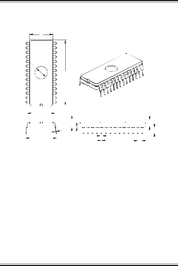
PIC16C5X
28-Lead Ceramic Dual In-line with Window (JW) – 600 mil (CERDIP)
E1
W 
D
n |
|
|
|
|
|
|
|
|
|
|
|
|
|
|
|
|
|
|
|
|
2 |
|
|
|
|
|
|
|
|
|
|
|
|
|
|
|
|
|
|
|
|
|
|
|
|
|
|
|
|
|
|
|
|
|
|
|
|
|
|
|
|
|
|
|
|
|
|
|
|
|
|
|
|
|
|
|
|
|
|
|
|
|
|
|
|
|
|
|
|
|
|
|
|
|
|
|
|
|
|
|
|
|
|
|
|
|
|
|
|
|
|
|
|
|
|
|
|
|
|
|
|
|
|
|
|
|
|
|
|
|
|
|
|
|
|
|
|
|
|
|
|
|
|
|
|
|
|
|
|
|
|
|
|
|
|
|
|
|
|
|
|
|
|
|
|
|
|
|
|
|
|
|
|
|
|
|
|
|
|
|
|
|
|
|
|
|
|
|
|||
|
|
|
|
|
|
|
|
|
|
|
|
|
|
|
|
|
|
|
|
|
|
|
|
|
|
|
|
|
|
|
|
|
|
|
|
|
|
|
|
|
|
|
|
|
|
|
|
|
|
|
|
|
|
|
|
|
|
|
|
|
|
|
|
|
|
|
|
|
|
|
|
|
|
|
|
|
|
|
|
|
|
|
|
|
|
|
|
|
|
|
|
|
|||
|
|
|
|
|
|
|
|
|
|
|
|
|
|
|
|
|
|
|
|
|
|
|
|
|
|
|
|
|
|
|
|
|
|
|
|
|
|
|
|
|
|
|
|
|
|
|
|
|
|
|
|
|
|
|
|
|
|
|
|
|
|
|
|
|
|
|
|
|
|
|
|
|
|
|
|
|
|
|
|
|
|
|
|
|
|
|
|
|
|
|
|
|
|||
|
|
|
|
|
|
|
|
|
|
|
|
|
|
|
|
|
|
|
|
|
|
|
|
|
|
|
|
|
|
|
|
|
|
|
|
|
|
|
|
|
|
|
|
|
|
|
|
|
|
|
|
|
|
|
|
|
|
|
|
|
|
|
|
|
|
|
|
|
|
|
|
|
|
|
|
|
|
|
|
|
|
|
|
|
|
|
|
|
|
|
|
|
|||
|
|
|
|
|
|
|
|
|
|
|
|
|
|
|
|
|
|
|
|
|
|
|
|
|
|
|
|
|
|
|
|
|
|
|
|
|
|
|
|
|
|
|
|
|
|
|
|
|
|
|
|
|
|
|
|
|
|
|
|
|
|
|
|
|
|
|
|
|
|
|
|
|
|
|
|
|
|
|
|
|
|
|
|
|
|
|
|
|
|
|
|
|
|||
|
|
|
|
|
|
|
|
|
|
|
|
|
|
|
|
|
|
|
|
|
|
|
|
|
|
|
|
|
|
|
|
|
|
|
|
|
|
|
|
|
|
|
|
|
|
|
|
|
|
|
|
|
|
|
|
|
|
|
|
|
|
|
|
|
|
|
|
|
|
|
|
|
|
|
|
|
|
|
|
|
|
|
|
|
|
|
|
|
|
|
|
|
|||
|
|
|
|
|
|
|
|
|
|
|
|
|
|
|
|
|
|
|
|
|
|
|
|
|
|
|
|
|
|
|
|
|
|
|
|
|
|
|
|
|
|
|
|
|
|
|
|
|
|
|
|
|
|
|
|
|
|
|
|
|
|
|
|
|
|
|
|
|
|
|
|
|
|
|
|
|
|
|
|
|
|
|
|
|
|
|
|
|
|
|
|
|
|||
|
|
|
|
|
|
|
|
|
|
|
|
|
|
|
|
|
|
1 |
|
|
|
|
|
|
|
|
|
|
|
|
|
|
|
|
|
|
|
|
|
|
|
|
|
|
|
|
|
|
|
|
|
|
|
|
|
|
|
|
|
|
|
|
|
|
|
|
|
|
|
|
|
|
|
|
|
|
|
|
|
|
|
|
|
|
|
|
|
|
|
|
|
||||
|
|
|
|
|
|
|
|
|
|
|
|
|
|
|
|
|
|
|
|
|
|
|
|
|
|
|
|
|
|
|
|
|
|
|
|
|
|
|
|
|
|
|
|
|
|
|
|
|
|
|
|
|
|
|
|
|
|
|
|
|
|
|
|
|
|
|
|
|
|
|
|
|
|
|
|
|
|
|
|
|
|||||||||||||||
|
|
|
|
|
|
|
|
|
|
|
|
|
|
|
|
|
|
|
|
|
|
|
|
|
|
|
|
|
|
|
|
|
|
|
|
|
|
|
|
|
|
|
|
|
|
|
|
|
|
|
|
|
|
|
|
|
|
|
|
|
|
|
|
|
|
|
|
|
|
|
|
|
|
|
|
|
|
||||||||||||||||||
|
|
|
|
|
|
|
|
|
|
|
|
|
|
|
|
|
|
|
|
|
|
|
|
|
|
|
|
|
|
|
|
|
|
|
|
|
|
|
|
|
|
|
|
|
|
|
|
|
|
|
|
|
|
|
|
|
|
|
|
|
|
|
|
|
|
|
|
|
|
|
|
|
|
|
|
|
|
||||||||||||||||||
|
|
|
|
|
|
|
|
|
|
|
|
|
|
|
|
|
|
|
|
|
|
|
|
|
|
|
|
|
|
|
|
|
|
|
|
|
|
|
|
|
|
|
|
|
|
|
|
|
|
|
|
|
|
|
|
|
|
|
|
|
|
|
|
|
|
|
|
|
|
|
|
|
|
|
|
|
|
|
|
|
|
|
|
|
|
|
|
|
|
|
|
|
|
|
|
|
|
|
|
|
|
|
|
|
|
|
E |
|
|
|
|
|
|
|
|
|
|
|
|
|
|
|
|
|
|
|
|
|
|
|
|
|
|
|
|
|
|
|
|
|
|
|
|
|
|
|
|
|
|
|
|
|
|
|
|
|
|
|
|
|
|
|
|
|
|
|
|
|
|
|
|
|
|
|
|
|
|
|
|
|
|
|
|
|
|
|
|
|
|
||
|
|
|
|
|
|
|
|
|
|
|
|
|
|
|
|
|
|
|
|
|
|
|
|
|
|
|
|
|
|
|
|
|
|
|
|
|
|
|
|
|
|
|
|
|
|
|
|
|
|
|
|
|
|
|
|
|
|
|
|
|
|
|
|
|
|
|
|
|
|
|
|
|
|
|
|
|
|
|
|
|
|
|
|
|
|
|
|
|
|
|
|
|
|||
|
|
|
|
|
|
|
|
|
|
|
|
|
|
|
|
|
|
|
|
|
|
|
|
|
|
|
|
|
|
|
|
|
|
|
|
|
|
|
|
|
|
|
|
|
|
|
|
|
|
|
|
|
|
|
|
|
|
|
|
|
|
|
|
|
|
|
|
|
|
|
|
|
|
|
|
|
|
|
|
|
|
|
|
|
|
|
|
|
|
|
|
|
|
|
|
|
|
|
|
|
|
|
|
|
|
|
|
|
|
|
|
|
|
|
|
|
|
|
|
|
|
|
|
|
|
|
|
|
|
|
|
|
|
|
|
|
|
|
|
|
|
|
|
|
|
|
|
|
|
|
|
|
|
|
|
|
|
|
|
|
|
|
|
|
|
|
|
|
|
|
|
|
|
|
|
|
|
|
|
|
|
|
|
|
|
|
|
|
|
|
|
|
|
|
|
|
|
|
|
|
|
|
|
|
|
|
|
|
|
|
|
|
|
|
|
|
|
|
A |
|
|
|
|
|
|
|
|
|
|
|
|
|
|
|
|
|
|
|
|
|
|
|
|
|
|
|
|
|
|
|
|
|
|
|
|
|
|
|
|
|
|
|
|
|
|
|
|
|
|
|
|
|
|
|
|
|
|
|
A2 |
|
|
||||||
|
|
|
|
|
|
|
|
|
|
|
|
|
|
|
|
|
|
|
|
|
|
|
|
|
|
|
|
|
|
|
|
|
|
|
|
|
|
|
|
|
|
|
|
|
|
|
|
|
|
|
|
|
|
|
|
|
|
|
|
|
|
|
|
|
|
|
|
|
|
|
|
|
|
|
|
|
|
|
|
|
|
|
|
|
|||||||||||
|
|
|
|
|
|
|
|
|
|
|
|
|
|
|
|
|
|
|
|
|
|
|
|
|
|
|
|
|
|
|
|
|
|
|
|
|
|
|
|
|
|
|
|
|
|
|
|
|
|
|
|
|
|
|
|
|
|
|
|
|
|
|
|
|
|
|
|
|
|
|
|
|
|
|
|
|
|
|
|
|
|
|
|
|
|
|
|
|
|
|
|
|
|
||
|
|
|
|
|
|
|
|
|
|
|
|
|
|
|
|
|
|
|
|
|
|
|
|
|
|
|
|
|
|
|
|
|
|
|
|
|
|
|
|
|
|
|
|
|
|
|
|
|
|
|
|
|
|
|
|
|
|
|
|
|
|
|
|
|
|
|
|
|
|
|
|
|
|
|
|
|
|
|
|
|
|
|
|
|
|
|
|
|
|
|
|
|
|
|
|
|
|
|
|
|
|
|
|
|
|
|
|
|
|
|
|
|
|
|
|
|
|
|
c |
|
|
|
|
|
|
|
|
|
|
|
|
|
|
|
|
|
|
|
|
|
|
|
|
|
|
|
|
|
|
|
|
|
|
|
|
|
|
|
|
|
|
|
|
|
|
|
|
|
|
|
|
|
|
|
|
|
|
|
|
|
|
|
|
|
|
L |
|||||
|
|
|
|
|
|
|
|
|
|
|
|
|
|
|
|
|
|
|
|
|
|
|
|
|
|
|
|
|
|
|
|
|
|
|
|
|
|
|
|
|
|
|
|
|
|
|
|
|
|
|
|
|
|
|
|
|
|
|
|
|
|
|
|
|
|
|
|
|
|
|
|
|
|
|
|
|
|
|
|
|
|
|
|
|
|
|
|
|
|
|
|
|
|
|
|
|
|
|
|
|
|
|
|
|
|
eB |
|
|
|
|
|
|
|
|
|
|
|
|
|
A1 |
|
|
|
|
|
|
|
|
|
|
|
|
|
|
|
|
|
|
|
|
|
|
|
|
|
|
|
|
|
|
|
|
B1 |
|
|
|
|
|
|
|
|
|
|
|
|
|
|
|
|
|
|
|
|
p |
|
|
|
|
|
|
|
|
|
||||||||
|
|
|
|
|
|
|
|
|
|
|
|
|
|
|
|
|
|
|
|
|
|
|
|
|
|
|
|
|
|
|
|
|
|
|
|
|
|
|
|
|
|
|
|
|
|
|
|
|
|
|
|
|
|
|
|
|
|
|
|
B |
|
|
|
|
|
|
|
|
|
|
|
|
|
|
|
|
|
|
|
|
|
|
|
|
|
|
|
|
|
||||||
|
|
|
|
|
|
|
|
|
|
|
|
|
|
|
|
|
|
|
|
|
|
|
|
|
|
|
|
|
|
|
|
|
|
|
|
|
|
|
|
|
|
|
|
|
|
|
|
|
|
|
|
|
|
|
|
|
|
|
|
|
|
|
|
|
|
|
|
|
|
|
|
|
|
|
|
|
|
|
|
|
|
|
|
|
|
|
|
|
|||||||
|
|
|
|
|
|
|
|
|
|
|
|
|
|
|
|
|
|
|
|
|
|
|
|
|
|
|
|
|
|
|
|
|
|
|
|
|
|
|
|
|
|
|
|
|
|
|
|
|
|
|
|
|
|
|
|
|
|
|
|
|
|
|
|
|
|
|
|
|
|
|
|
|
|
|
|
|
|
|
|
|
|
|
|
|
|
|
|
|
|
|
|
|
|
|
|
|
|
|
|
|
|
|
|
|
|
|
|
|
|
|
|
|
|
|
|
|
|
|
Units |
|
|
|
|
|
|
|
|
|
|
|
INCHES* |
|
|
|
|
|
|
|
|
|
|
|
|
|
|
|
|
|
|
|
|
|
|
|
|
|
MILLIMETERS |
|
|
|
|
|
|
||||||||||||||||||||||||||||
|
|
|
|
|
|
|
|
|
|
|
|
|
Dimension Limits |
|
|
|
MIN |
|
|
|
NOM |
|
|
|
|
MAX |
|
|
|
MIN |
|
|
|
NOM |
|
MAX |
|||||||||||||||||||||||||||||||||||||||||||||||||||||||||||
Number of Pins |
|
|
|
|
|
|
n |
|
|
|
|
|
|
|
|
|
|
|
28 |
|
|
|
|
|
|
|
|
|
|
|
|
|
|
|
|
|
|
|
|
|
|
|
|
|
|
|
28 |
|
|
|
|
|
|
|
|||||||||||||||||||||||||||||||||||||||||
Pitch |
|
|
|
|
|
|
p |
|
|
|
|
|
|
|
|
|
|
|
.100 |
|
|
|
|
|
|
|
|
|
|
|
|
|
|
|
|
|
|
|
|
|
|
|
|
|
|
|
2.54 |
|
|
|
|
|
|
|
|||||||||||||||||||||||||||||||||||||||||
Top to Seating Plane |
|
|
|
|
|
|
A |
.195 |
|
.210 |
|
.225 |
4.95 |
|
5.33 |
|
5.72 |
||||||||||||||||||||||||||||||||||||||||||||||||||||||||||||||||||||||||||||||
Ceramic Package Height |
|
|
|
|
|
|
A2 |
.155 |
|
.160 |
.165 |
3.94 |
|
4.06 |
|
4.19 |
|||||||||||||||||||||||||||||||||||||||||||||||||||||||||||||||||||||||||||||||
Standoff |
|
|
|
|
|
|
A1 |
.015 |
|
.038 |
.060 |
0.38 |
|
0.95 |
|
1.52 |
|||||||||||||||||||||||||||||||||||||||||||||||||||||||||||||||||||||||||||||||
Shoulder to Shoulder Width |
|
|
|
|
|
|
E |
.595 |
|
.600 |
.625 |
15.11 |
|
15.24 |
|
15.88 |
|||||||||||||||||||||||||||||||||||||||||||||||||||||||||||||||||||||||||||||||
Ceramic Pkg. Width |
|
|
|
|
|
|
E1 |
.514 |
|
.520 |
.526 |
13.06 |
|
13.21 |
|
13.36 |
|||||||||||||||||||||||||||||||||||||||||||||||||||||||||||||||||||||||||||||||
Overall Length |
|
|
|
|
|
|
D |
1.430 |
|
1.460 |
|
1.490 |
36.32 |
|
37.08 |
|
37.85 |
||||||||||||||||||||||||||||||||||||||||||||||||||||||||||||||||||||||||||||||
Tip to Seating Plane |
|
|
|
|
|
|
L |
.125 |
|
.138 |
.150 |
3.18 |
|
3.49 |
|
3.81 |
|||||||||||||||||||||||||||||||||||||||||||||||||||||||||||||||||||||||||||||||
Lead Thickness |
|
|
|
|
|
|
c |
.008 |
|
.010 |
.012 |
0.20 |
|
0.25 |
|
0.30 |
|||||||||||||||||||||||||||||||||||||||||||||||||||||||||||||||||||||||||||||||
Upper Lead Width |
|
|
|
|
|
|
B1 |
.050 |
|
.058 |
.065 |
1.27 |
|
1.46 |
|
1.65 |
|||||||||||||||||||||||||||||||||||||||||||||||||||||||||||||||||||||||||||||||
Lower Lead Width |
|
|
|
|
|
|
B |
.016 |
|
.020 |
.023 |
0.41 |
0.51 |
|
0.58 |
||||||||||||||||||||||||||||||||||||||||||||||||||||||||||||||||||||||||||||||||
Overall Row Spacing |
§ |
|
|
|
eB |
.610 |
|
.660 |
.710 |
15.49 |
|
16.76 |
|
18.03 |
|||||||||||||||||||||||||||||||||||||||||||||||||||||||||||||||||||||||||||||||||
Window Diameter |
|
|
|
|
|
|
W |
.270 |
|
.280 |
.290 |
6.86 |
|
7.11 |
|
7.37 |
|||||||||||||||||||||||||||||||||||||||||||||||||||||||||||||||||||||||||||||||
* Controlling Parameter |
|
|
|
|
|
|
|
|
|
|
|
|
|
|
|
|
|
|
|
|
|
|
|
|
|
|
|
|
|
|
|
|
|
|
|
|
|
|
|
|
|
|
|
|
|
|
|
|
|
|
|
|
|
|
|
|
|
|
|
|
|
|
|
|
|
|
|
|
|
|
|
|
|
|
|
|
|
|
|
||||||||||||||||
§ Significant Characteristic |
|
|
|
|
|
|
|
|
|
|
|
|
|
|
|
|
|
|
|
|
|
|
|
|
|
|
|
|
|
|
|
|
|
|
|
|
|
|
|
|
|
|
|
|
|
|
|
|
|
|
|
|
|
|
|
|
|
|
|
|
|
|
|
|
|
|
|
|
|
|
|
|
|
|
|
|
|
|
|
||||||||||||||||
JEDEC Equivalent: MO-103
Drawing No. C04-013
ã 2002 Microchip Technology Inc. |
Preliminary |
DS30453D-page 181

PIC16C5X
NOTES:
DS30453D-page 182 |
Preliminary |
ã 2002 Microchip Technology Inc. |

PIC16C5X
APPENDIX A: COMPATIBILITY
To convert code written for PIC16CXX to PIC16C5X, the user should take the following steps:
1.Check any CALL, GOTO or instructions that modify the PC to determine if any program memory page select operations (PA2, PA1, PA0 bits) need to be made.
2.Revisit any computed jump operations (write to PC or add to PC, etc.) to make sure page bits are set properly under the new scheme.
3.Eliminate any special function register page switching. Redefine data variables to reallocate them.
4.Verify all writes to STATUS, OPTION, and FSR registers since these have changed.
5.Change RESET vector to proper value for processor used.
6.Remove any use of the ADDLW, RETURN and SUBLW instructions.
7.Rewrite any code segments that use interrupts.
ã 2002 Microchip Technology Inc. |
Preliminary |
DS30453D-page 183

PIC16C5X
NOTES:
DS30453D-page 184 |
Preliminary |
ã 2002 Microchip Technology Inc. |

PIC16C5X
INDEX |
|
A |
|
Absolute Maximum Ratings |
|
PIC16C54/55/56/57 .................................................... |
67 |
PIC16C54A ............................................................... |
103 |
PIC16C54C/CR54C/C55A/C56A/CR56A/C57C/CR57C/ |
|
C58B/CR58B ............................................................ |
131 |
PIC16C54C/CR54C/C55A/C56A/CR56A/C57C/CR57C/ |
|
C58B/CR58B-40 ....................................................... |
155 |
PIC16CR54A .............................................................. |
79 |
ADDWF ............................................................................... |
51 |
ALU ....................................................................................... |
9 |
ANDLW ............................................................................... |
51 |
ANDWF ............................................................................... |
51 |
Applications........................................................................... |
5 |
Architectural Overview .......................................................... |
9 |
Assembler |
|
MPASM Assembler ..................................................... |
61 |
B |
|
Block Diagram |
|
On-Chip Reset Circuit ................................................. |
20 |
PIC16C5X Series........................................................ |
10 |
Timer0 ......................................................................... |
37 |
TMR0/WDT Prescaler................................................. |
41 |
Watchdog Timer.......................................................... |
46 |
Brown-Out Protection Circuit .............................................. |
23 |
BSF ..................................................................................... |
52 |
BTFSC ................................................................................ |
52 |
BTFSS ................................................................................ |
52 |
C |
|
CALL ............................................................................. |
31, 53 |
Carry (C) bit .................................................................... |
9, 29 |
Clocking Scheme ................................................................ |
13 |
CLRF................................................................................... |
53 |
CLRW ................................................................................. |
53 |
CLRWDT............................................................................. |
53 |
CMOS Technology................................................................ |
1 |
Code Protection ............................................................ |
43, 47 |
COMF ................................................................................. |
54 |
Compatibility ..................................................................... |
183 |
Configuration Bits................................................................ |
44 |
D |
|
Data Memory Organization ................................................. |
26 |
DC Characteristics |
|
PIC16C54/55/56/57 |
|
Commercial................................................... |
68, 71 |
Extended....................................................... |
70, 72 |
Industrial ....................................................... |
69, 71 |
PIC16C54A |
|
Commercial............................................... |
104, 109 |
Extended................................................... |
106, 109 |
Industrial ................................................... |
104, 109 |
PIC16C54C/C55A/C56A/C57C/C58B-40 |
|
Commercial............................................... |
157, 158 |
PIC16C54C/CR54C/C55A/C56A/CR56A/C57C/CR57C/ |
|
C58B/CR58B |
|
Commercial............................................... |
134, 138 |
Extended................................................... |
137, 138 |
Industrial ................................................... |
134, 138 |
PIC16CR54A |
|
Commercial .................................................. |
80, 83 |
Extended ...................................................... |
82, 84 |
Industrial ....................................................... |
80, 83 |
PIC16LV54A |
|
Commercial .............................................. |
108, 109 |
Industrial ................................................... |
108, 109 |
DECF .................................................................................. |
54 |
DECFSZ ............................................................................. |
54 |
Development Support ......................................................... |
61 |
Device Characterization |
|
PIC16C54/55/56/57/CR54A ....................................... |
91 |
PIC16C54A............................................................... |
117 |
PIC16C54C/C55A/C56A/C57C/C58B-40 ................. |
165 |
Device Reset Timer (DRT) ................................................. |
23 |
Device Varieties.................................................................... |
7 |
Digit Carry (DC) bit ......................................................... |
9, 29 |
DRT .................................................................................... |
23 |
E |
|
Electrical Specifications |
|
PIC16C54/55/56/57 .................................................... |
67 |
PIC16C54A............................................................... |
103 |
PIC16C54C/CR54C/C55A/C56A/CR56A/C57C/CR57C/ |
|
C58B/CR58B ............................................................ |
131 |
PIC16C54C/CR54C/C55A/C56A/CR56A/C57C/CR57C/ |
|
C58B/CR58B-40....................................................... |
155 |
PIC16CR54A .............................................................. |
79 |
Errata .................................................................................... |
3 |
External Power-On Reset Circuit........................................ |
21 |
F |
|
Family of Devices |
|
PIC16C5X..................................................................... |
6 |
FSR Register ...................................................................... |
33 |
Value on reset............................................................. |
20 |
G |
|
General Purpose Registers |
|
Value on reset............................................................. |
20 |
GOTO ........................................................................... |
31, 55 |
H |
|
High-Performance RISC CPU .............................................. |
1 |
I |
|
I/O Interfacing ..................................................................... |
35 |
I/O Ports ............................................................................. |
35 |
I/O Programming Considerations ....................................... |
36 |
ICEPIC In-Circuit Emulator ................................................. |
62 |
ID Locations.................................................................. |
43, 47 |
INCF ................................................................................... |
55 |
INCFSZ............................................................................... |
55 |
INDF Register ..................................................................... |
33 |
Value on reset............................................................. |
20 |
Indirect Data Addressing .................................................... |
33 |
Instruction Cycle ................................................................. |
13 |
Instruction Flow/Pipelining .................................................. |
13 |
Instruction Set Summary .................................................... |
49 |
IORLW ................................................................................ |
56 |
IORWF................................................................................ |
56 |
K |
|
KeeLoq Evaluation and Programming Tools ...................... |
64 |
ã 2002 Microchip Technology Inc. |
Preliminary |
DS30453D-page 185

PIC16C5X
L |
|
|
Loading of PC ..................................................................... |
|
31 |
M |
|
|
MCLR Reset |
|
|
Register values on ...................................................... |
|
20 |
Memory Map |
|
|
PIC16C54/CR54/C55.................................................. |
|
25 |
PIC16C56/CR56 ......................................................... |
|
25 |
PIC16C57/CR57/C58/CR58 ....................................... |
|
25 |
Memory Organization.......................................................... |
|
25 |
MOVF.................................................................................. |
|
56 |
MOVLW............................................................................... |
|
56 |
MOVWF .............................................................................. |
|
57 |
MPLAB C17 and MPLAB C18 C Compilers........................ |
|
61 |
MPLAB ICD In-Circuit Debugger......................................... |
|
63 |
MPLAB ICE High Performance Universal In-Circuit Emulator |
||
with MPLAB IDE.................................................................. |
|
62 |
MPLAB Integrated Development Environment Software .... |
61 |
|
MPLINK Object Linker/MPLIB Object Librarian .................. |
|
62 |
N |
|
|
NOP .................................................................................... |
|
57 |
O |
|
|
One-Time-Programmable (OTP) Devices............................. |
|
7 |
OPTION .............................................................................. |
|
57 |
OPTION Register ................................................................ |
|
30 |
Value on reset ............................................................. |
|
20 |
Oscillator Configurations ..................................................... |
|
15 |
Oscillator Types |
|
|
HS ............................................................................... |
|
15 |
LP................................................................................ |
|
15 |
RC ............................................................................... |
|
15 |
XT ............................................................................... |
|
15 |
P |
|
|
PA0 bit................................................................................. |
|
29 |
PA1 bit................................................................................. |
|
29 |
Paging ................................................................................. |
|
31 |
PC ....................................................................................... |
|
31 |
Value on reset ............................................................. |
|
20 |
PD bit ............................................................................ |
19, 29 |
|
Peripheral Features............................................................... |
|
1 |
PICDEM 1 Low Cost PICmicro Demonstration Board ........ |
|
63 |
PICDEM 17 Demonstration Board ...................................... |
|
64 |
PICDEM 2 Low Cost PIC16CXX Demonstration Board...... |
|
63 |
PICDEM 3 Low Cost PIC16CXXX Demonstration Board ... |
64 |
|
PICSTART Plus Entry Level Development Programmer .... |
63 |
|
Pin Configurations................................................................. |
|
2 |
Pinout Description - PIC16C54, PIC16CR54, PIC16C56, |
||
PIC16CR56, PIC16C58, PIC16CR58 ................................. |
|
11 |
Pinout Description - PIC16C55, PIC16C57, PIC16CR57 ... |
12 |
|
PORTA................................................................................ |
|
35 |
Value on reset ............................................................. |
|
20 |
PORTB................................................................................ |
|
35 |
Value on reset ............................................................. |
|
20 |
PORTC................................................................................ |
|
35 |
Value on reset ............................................................. |
|
20 |
Power-Down Mode.............................................................. |
|
47 |
Power-On Reset (POR) ...................................................... |
|
21 |
Register values on ...................................................... |
|
20 |
Prescaler ............................................................................. |
|
40 |
PRO MATE II Universal Device Programmer ..................... |
|
63 |
Program Counter................................................................. |
|
31 |
Program Memory Organization........................................... |
25 |
Program Verification/Code Protection ................................ |
47 |
Q |
|
Q cycles .............................................................................. |
13 |
Quick-Turnaround-Production (QTP) Devices...................... |
7 |
R |
|
RC Oscillator....................................................................... |
17 |
Read Only Memory (ROM) Devices ..................................... |
7 |
Read-Modify-Write.............................................................. |
36 |
Register File Map |
|
PIC16C54, PIC16CR54, PIC16C55, PIC16C56, |
|
PIC16CR56 ................................................................ |
26 |
PIC16C57/CR57 ......................................................... |
27 |
PIC16C58/CR58 ......................................................... |
27 |
Registers |
|
Special Function ......................................................... |
28 |
Value on reset............................................................. |
20 |
Reset .................................................................................. |
19 |
Reset on Brown-Out ........................................................... |
23 |
RETLW ............................................................................... |
57 |
RLF ..................................................................................... |
58 |
RRF .................................................................................... |
58 |
S |
|
Serialized Quick-Turnaround-Production (SQTP) Devices... 7 |
|
SLEEP .................................................................... |
43, 47, 58 |
Software Simulator (MPLAB SIM) ...................................... |
62 |
Special Features of the CPU .............................................. |
43 |
Special Function Registers ................................................. |
28 |
Stack................................................................................... |
32 |
STATUS Register ........................................................... |
9, 29 |
Value on reset............................................................. |
20 |
SUBWF............................................................................... |
59 |
SWAPF ............................................................................... |
59 |
T |
|
Timer0 |
|
Switching Prescaler Assignment ................................ |
40 |
Timer0 (TMR0) Module............................................... |
37 |
TMR0 register - Value on reset................................... |
20 |
TMR0 with External Clock .......................................... |
39 |
Timing Diagrams and Specifications |
|
PIC16C54/55/56/57 .................................................... |
74 |
PIC16C54A............................................................... |
111 |
PIC16C54C/CR54C/C55A/C56A/CR56A/C57C/CR57C/ |
|
C58B/CR58B ............................................................ |
140 |
PIC16C54C/CR54C/C55A/C56A/CR56A/C57C/CR57C/ |
|
C58B/CR58B-40 ....................................................... |
160 |
PIC16CR54A .............................................................. |
86 |
Timing Parameter Symbology and Load Conditions |
|
PIC16C54/55/56/57 .................................................... |
73 |
PIC16C54A............................................................... |
110 |
PIC16C54C/CR54C/C55A/C56A/CR56A/C57C/CR57C/ |
|
C58B/CR58B ............................................................ |
139 |
PIC16C54C/CR54C/C55A/C56A/CR56A/C57C/CR57C/ |
|
C58B/CR58B-40 ....................................................... |
159 |
PIC16CR54A .............................................................. |
85 |
TO bit ............................................................................ |
19, 29 |
TRIS.................................................................................... |
59 |
TRIS Registers ................................................................... |
35 |
Value on reset............................................................. |
20 |
DS30453D-page 186 |
Preliminary |
ã 2002 Microchip Technology Inc. |

PIC16C5X
U |
|
UV Erasable Devices ............................................................ |
7 |
W |
|
W Register |
|
Value on reset ............................................................. |
20 |
Wake-up from SLEEP ................................................... |
19, 47 |
Watchdog Timer (WDT) ................................................ |
43, 46 |
Period.......................................................................... |
46 |
Programming Considerations ..................................... |
46 |
Register values on reset ............................................. |
20 |
WWW, On-Line Support ....................................................... |
3 |
X |
|
XORLW ............................................................................... |
60 |
XORWF............................................................................... |
60 |
Z |
|
Zero (Z) bit ...................................................................... |
9, 29 |
ã 2002 Microchip Technology Inc. |
Preliminary |
DS30453D-page 187

PIC16C5X
NOTES:
DS30453D-page 188 |
Preliminary |
ã 2002 Microchip Technology Inc. |