
- •Trademarks
- •Devices Included in this Data Sheet:
- •High-Performance RISC CPU:
- •Peripheral Features:
- •CMOS Technology:
- •Pin Diagrams
- •Device Differences
- •Table of Contents
- •Most Current Data Sheet
- •Errata
- •Customer Notification System
- •1.0 General Description
- •1.1 Applications
- •2.0 PIC16C5X Device Varieties
- •2.1 UV Erasable Devices (EPROM)
- •2.5 Read Only Memory (ROM) Devices
- •3.0 Architectural Overview
- •FIGURE 3-1: PIC16C5X Series Block Diagram
- •3.1 Clocking Scheme/Instruction Cycle
- •3.2 Instruction Flow/Pipelining
- •4.0 Oscillator Configurations
- •4.1 Oscillator Types
- •4.2 Crystal Oscillator/Ceramic Resonators
- •FIGURE 4-1: Crystal/Ceramic Resonator Operation (HS, XT or LP OSC Configuration)
- •FIGURE 4-2: External Clock Input Operation (HS, XT or LP OSC Configuration)
- •TABLE 4-1: Capacitor Selection For Ceramic Resonators - PIC16C5X, PIC16CR5X
- •TABLE 4-2: Capacitor Selection For Crystal Oscillator - PIC16C5X, PIC16CR5X
- •4.3 External Crystal Oscillator Circuit
- •4.4 RC Oscillator
- •FIGURE 4-5: RC Oscillator Mode
- •5.0 Reset
- •TABLE 5-1: Status Bits and Their Significance
- •TABLE 5-2: Summary of REgisters Associated with RESET
- •FIGURE 5-1: Simplified Block Diagram of On-Chip Reset Circuit
- •FIGURE 5-2: External Power-On Reset Circuit (For Slow Vdd Power-Up)
- •FIGURE 5-3: Time-Out Sequence on Power-Up (MCLR Not Tied to Vdd)
- •FIGURE 5-4: Time-Out Sequence on Power-Up (MCLR Tied to Vdd): Fast Vdd Rise Time
- •FIGURE 5-5: Time-Out Sequence on Power-Up (MCLR Tied to Vdd): Slow Vdd Rise Time
- •5.2 Device Reset Timer (DRT)
- •FIGURE 5-6: External Brown-Out Protection Circuit 1
- •FIGURE 5-7: External Brown-Out Protection Circuit 2
- •FIGURE 5-8: EXTERNAL BROWN-OUT PROTECTION CIRCUIT 3
- •6.0 Memory Organization
- •6.1 Program Memory Organization
- •FIGURE 6-1: PIC16C54/CR54/C55 Program Memory Map and Stack
- •FIGURE 6-3: PIC16C57/CR57/C58/ CR58 Program Memory Map and Stack
- •6.2 Data Memory Organization
- •FIGURE 6-5: PIC16C57/CR57 Register File Map
- •FIGURE 6-6: PIC16C58/CR58 Register File Map
- •6.3 STATUS Register
- •6.4 OPTION Register
- •6.5 Program Counter
- •6.6 Stack
- •6.7 Indirect Data Addressing; INDF and FSR Registers
- •FIGURE 6-10: Direct/Indirect Addressing
- •7.0 I/O Ports
- •7.1 PORTA
- •7.2 PORTB
- •7.3 PORTC
- •7.4 TRIS Registers
- •7.5 I/O Interfacing
- •FIGURE 7-1: Equivalent Circuit for a Single I/O Pin
- •7.6 I/O Programming Considerations
- •FIGURE 7-2: Successive I/O Operation
- •8.0 Timer0 Module and TMR0 Register
- •FIGURE 8-2: Electrical Structure of T0CKI Pin
- •8.1 Using Timer0 with an External Clock
- •FIGURE 8-5: Timer0 Timing With External Clock
- •8.2 Prescaler
- •FIGURE 8-6: Block Diagram of the Timer0/WDT Prescaler
- •9.0 Special Features of the CPU
- •9.1 Configuration Bits
- •9.2 Watchdog Timer (WDT)
- •9.4 Program Verification/Code Protection
- •9.5 ID Locations
- •10.0 Instruction Set Summary
- •FIGURE 10-1: General Format for Instructions
- •11.0 Development Support
- •11.1 MPLAB Integrated Development Environment Software
- •11.2 MPASM Assembler
- •11.3 MPLAB C17 and MPLAB C18 C Compilers
- •11.4 MPLINK Object Linker/ MPLIB Object Librarian
- •11.5 MPLAB SIM Software Simulator
- •11.9 PRO MATE II Universal Device Programmer
- •11.10 PICSTART Plus Entry Level Development Programmer
- •11.11 PICDEM 1 Low Cost PICmicro Demonstration Board
- •11.12 PICDEM 2 Low Cost PIC16CXX Demonstration Board
- •11.13 PICDEM 3 Low Cost PIC16CXXX Demonstration Board
- •11.14 PICDEM 17 Demonstration Board
- •12.0 Electrical Characteristics - PIC16C54/55/56/57
- •12.6 Timing Parameter Symbology and Load Conditions
- •12.7 Timing Diagrams and Specifications
- •FIGURE 12-2: External Clock Timing - PIC16C54/55/56/57
- •TABLE 12-1: EXTERNAL CLOCK TIMING REQUIREMENTS - PIC16C54/55/56/57
- •FIGURE 12-4: Reset, Watchdog Timer, and Device Reset Timer Timing - PIC16C54/55/56/57
- •TABLE 12-3: Reset, Watchdog Timer, and Device Reset Timer - PIC16C54/55/56/57
- •FIGURE 12-5: Timer0 Clock Timings - PIC16C54/55/56/57
- •TABLE 12-4: Timer0 Clock Requirements - PIC16C54/55/56/57
- •13.0 Electrical Characteristics - PIC16CR54A
- •13.5 Timing Parameter Symbology and Load Conditions
- •FIGURE 13-1: Load Conditions For Device Timing Specifications - PIC16CR54A
- •13.6 Timing Diagrams and Specifications
- •FIGURE 13-2: External Clock Timing - PIC16CR54A
- •TABLE 13-1: External Clock Timing Requirements - PIC16CR54A
- •FIGURE 13-3: CLKOUT and I/O Timing - PIC16CR54A
- •TABLE 13-2: CLKOUT and I/O Timing Requirements - PIC16CR54A
- •FIGURE 13-4: Reset, Watchdog Timer, and Device Reset Timer Timing - PIC16CR54A
- •TABLE 13-3: Reset, Watchdog Timer, and Device Reset Timer - PIC16CR54A
- •FIGURE 13-5: Timer0 Clock Timings - PIC16CR54A
- •14.0 Device Characterization - PIC16C54/55/56/57/CR54A
- •FIGURE 14-1: Typical RC Oscillator Frequency vs. Temperature
- •FIGURE 14-5: Typical Ipd vs. Vdd, Watchdog Disabled
- •FIGURE 14-6: Maximum Ipd vs. Vdd, Watchdog Disabled
- •FIGURE 14-7: Typical Ipd vs. Vdd, Watchdog Enabled
- •FIGURE 14-8: Maximum Ipd vs. Vdd, Watchdog Enabled
- •FIGURE 14-9: Vth (Input Threshold Voltage) of I/O Pins vs. Vdd
- •FIGURE 14-10: Vih, Vil of MCLR, T0CKI and OSC1 (RC Mode) vs. Vdd
- •FIGURE 14-11: Vth (Input Threshold Voltage) of OSC1 Input (XT, HS, and LP modes) vs. Vdd
- •FIGURE 14-12: Typical Idd vs. Frequency (External Clock, 25°C)
- •FIGURE 14-15: WDT Timer Time-out Period vs. Vdd(1)
- •FIGURE 14-16: Transconductance (gm) of HS Oscillator vs. Vdd
- •FIGURE 14-17: Transconductance (gm) of LP Oscillator vs. Vdd
- •FIGURE 14-18: Transconductance (gm) of XT Oscillator vs. Vdd
- •15.0 Electrical Characteristics - PIC16C54A
- •15.5 Timing Parameter Symbology and Load Conditions
- •15.6 Timing Diagrams and Specifications
- •Figure 15-2: External Clock Timing - PIC16C54A
- •TABLE 15-1: External Clock Timing Requirements - PIC16C54A
- •FIGURE 15-4: Reset, Watchdog Timer, and Device Reset Timer Timing - PIC16C54A
- •TABLE 15-3: Reset, Watchdog Timer, and Device Reset Timer - PIC16C54A
- •FIGURE 15-5: Timer0 Clock Timings - PIC16C54A
- •16.0 Device Characterization - PIC16C54A
- •FIGURE 16-1: Typical RC Oscillator Frequency vs. Temperature
- •FIGURE 16-7: Vth (Input Threshold Voltage) of I/O Pins - Vdd
- •FIGURE 16-9: Vih, Vil of MCLR, T0CKI and OSC1 (in RC Mode) vs. Vdd
- •FIGURE 16-10: Typical Idd vs. Frequency (WDT disabled, RC Mode @ 20 pF, 25°C)
- •FIGURE 16-12: Typical Idd vs. Frequency (WDT Disabled, RC Mode @ 100 pF, 25°C)
- •FIGURE 16-14: Typical Idd vs. Frequency (WDT Disabled, RC Mode @ 300 pF, 25°C)
- •FIGURE 16-16: WDT Timer Time-out Period vs. Vdd(1)
- •FIGURE 16-17: Transconductance (gm) of HS Oscillator vs. Vdd
- •FIGURE 16-18: Transconductance (gm) of LP Oscillator vs. Vdd
- •FIGURE 16-19: Transconductance (gm) of XT Oscillator vs. Vdd
- •17.0 Electrical Characteristics - PIC16C54C/CR54C/C55A/C56A/CR56A/ C57C/CR57C/C58B/CR58B
- •17.4 Timing Parameter Symbology and Load Conditions
- •17.5 Timing Diagrams and Specifications
- •FIGURE 17-6: External Clock Timing - PIC16C5X, PIC16CR5X
- •FIGURE 17-8: Reset, Watchdog Timer, and Device Reset Timer Timing - PIC16C5X, PIC16CR5X
- •TABLE 17-3: Reset, Watchdog Timer, and Device Reset Timer - PIC16C5X, PIC16CR5X
- •FIGURE 17-9: Timer0 Clock Timings - PIC16C5X, PIC16CR5X
- •TABLE 17-4: Timer0 Clock Requirements - PIC16C5X, PIC16CR5X
- •FIGURE 18-1: Typical RC Oscillator Frequency vs. Temperature
- •FIGURE 18-5: Typical Ipd vs. Vdd, Watchdog Disabled (25°C)
- •FIGURE 18-6: Typical Ipd vs. Vdd, Watchdog Enabled (25°C)
- •FIGURE 18-8: Vth (Input Threshold Trip Point Voltage) of I/O Pins vs. Vdd
- •FIGURE 18-9: Vih, Vil of MCLR, T0CKI and OSC1 (in RC Mode) vs. Vdd
- •FIGURE 18-11: Typical Idd vs. Frequency (WDT disabled, RC Mode @ 20 pF, 25°C)
- •FIGURE 18-12: Typical Idd vs. Frequency (WDT Disabled, RC Mode @ 100 pF, 25°C)
- •FIGURE 18-13: Typical Idd vs. Frequency (WDT Disabled, RC Mode @ 300 pF, 25°C)
- •FIGURE 18-14: WDT Timer Time-out Period vs. Vdd(1)
- •TABLE 18-2: Input Capacitance
- •19.0 Electrical Characteristics - PIC16C54C/C55A/C56A/C57C/C58B 40MHz
- •19.3 Timing Parameter Symbology and Load Conditions
- •FIGURE 19-2: Load Conditions For Device Timing Specifications - PIC16C54C/C55A/C56A/C57C/C58B-40
- •19.4 Timing Diagrams and Specifications
- •TABLE 19-2: CLKOUT and I/O Timing Requirements - PIC16C5X-40
- •FIGURE 19-5: Reset, Watchdog Timer, and Device Reset Timer Timing - PIC16C5X-40
- •TABLE 19-3: Reset, Watchdog Timer, and Device Reset Timer - PIC16C5X-40
- •FIGURE 19-6: Timer0 Clock Timings - PIC16C5X-40
- •TABLE 19-4: Timer0 Clock Requirements PIC16C5X-40
- •FIGURE 20-1: Typical Ipd vs. Vdd, Watchdog Disabled (25°C)
- •FIGURE 20-2: Typical Ipd vs. Vdd, Watchdog Enabled (25°C)
- •FIGURE 20-4: Vth (Input Threshold Trip Point Voltage) of I/O Pins vs. Vdd
- •FIGURE 20-5: Vth (Input Threshold Trip Point Voltage) of OSC1 Input (HS mode) vs. Vdd
- •FIGURE 20-6: Typical Idd vs. Vdd (40 MHz, WDT disabled, HS Mode, 70°C)
- •FIGURE 20-7: WDT Timer Time-out Period vs. Vdd(1)
- •TABLE 20-1: Input Capacitance
- •FIGURE 20-8: Ioh vs. Voh, Vdd = 5 V
- •21.0 Packaging Information
- •21.1 Package Marketing Information
- •Package Marking Information (Cont’d)
- •On-Line Support
- •Connecting to the Microchip Internet Web Site
- •Systems Information and Upgrade Hot Line
- •Reader Response
- •Product Identification System

PIC16C5X
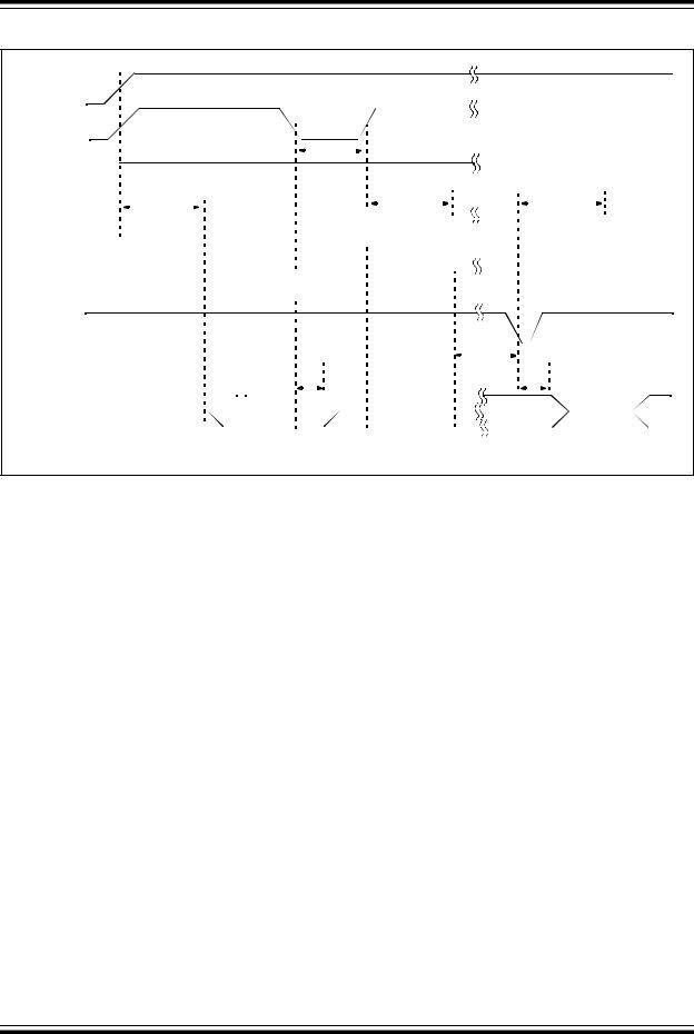
FIGURE 15-4: RESET, WATCHDOG TIMER, AND DEVICE RESET TIMER TIMING - PIC16C54A
|
VDD |
|
|
|
|
|
|
|
|
|
|
|
|
|
|
|
|
|
|
|
|
|
|
|
|
|
|
|
|
|
|
|
|
|
|
|
|
|
|||||||
|
|
|
|
|
|
|
|
|
|
|
|
|
|
|
|
|
|
|
|
|
|
|
|
|
|
|
|
|
|
|
|
|
|
|
|
|
|
|
|
|
|
|
|
||
|
|
|
|
|
|
|
|
|
|
|
|
|
|
|
|
|
|
|
|
|
|
|
|
|
|
|
|
|
|
|
|
|
|
|
|
|
|
|
|
|
|
|
|
|
|
|
MCLR |
|
|
|
|
|
|
|
|
|
|
|
|
30 |
|
|
|
|
|
|
|
|
|
|
|
|
|
|
|
|
|
|
|
|
|
|
|
|
|
|
|
|
|||
|
|
|
|
|
|
|
|
|
|
|
|
|
|
|
|
|
|
|
|
|
|
|
|
|
|
|
|
|
|
|
|
|
|
|
|
|
|
|
|
||||||
|
|
|
|
|
|
|
|
|
|
|
|
|
|
|
|
|
|
|
|
|
|
|
|
|
|
|
|
|
|
|
|
|
|
|
|
|
|
|
|
|
|
|
|
||
|
|
|
|
|
|
|
|
|
|
|
|
|
|
|
|
|
|
|
|
|
|
|
|
|
|
|
|
|
|
|
|
|
|
|
|
|
|
|
|
||||||
Internal |
|
|
|
|
|
|
|
|
|
|
|
|
|
|
|
|
|
|
|
|
|
|
|
|
|
|
|
|
|
|
|
|
|
|
|
|
|
|
|
|
|||||
|
POR |
|
|
32 |
|
32 |
|
|
|
|
|
||||||||||||||||||||||||||||||||||
|
32 |
|
|
|
|
|
|
|
|||||||||||||||||||||||||||||||||||||
|
|
|
|
|
|
|
|
|
|
|
|
|
|
|
|
|
|
|
|
|
|
|
|
|
|
|
|
|
|
|
|
|
|
|
|
|
|
||||||||
|
|
|
|
|
|
|
|
|
|
|
|
|
|
|
|
|
|
|
|
|
|
|
|
|
|
|
|
|
|
|
|
|
|
|
|
|
|
||||||||
|
DRT |
|
|
|
|
|
|
|
|
|
|
|
|
|
|
|
|
|
|
|
|
|
|
|
|
|
|
|
|
|
|
|
|
|
|
|
|
|
|||||||
|
|
|
|
|
|
|
|
|
|
|
|
|
|
|
|
|
|
|
|
|
|
|
|
|
|
|
|
|
|
|
|
|
|
|
|
|
|
||||||||
Time-out |
|
|
|
|
|
|
|
|
|
|
|
|
|
|
|
|
|
|
|
|
|
|
|
|
|
|
|
|
|
|
|
|
|
|
|
|
|
|
|||||||
Internal |
|
|
|
|
|
|
|
|
|
|
|
|
|
|
|
|
|
|
|
|
|
|
|
|
|
|
|
|
|
|
|
|
|
|
|
|
|
||||||||
|
|
|
|
|
|
|
|
|
|
|
|
|
|
|
|
|
|
|
|
|
|
|
|
|
|
|
|
|
|
|
|
|
|
|
|
|
|||||||||
RESET |
|
|
|
|
|
|
|
|
|
|
|
|
|
|
|
|
|
|
|
|
|
|
|
|
|
|
|
|
|
|
|
|
|
|
|
|
|
||||||||
|
|
|
|
|
|
|
|
|
|
|
|
|
|
|
|
|
|
|
|
|
|
|
|
|
|
|
|
|
|
|
|
|
|
|
|
|
|
|
|
||||||
Watchdog |
|
|
|
|
|
|
|
|
|
|
|
|
|
|
|
|
|
|
|
|
|
|
|
|
|
|
|
|
|
|
|
|
|
|
|
|
|
||||||||
|
Timer |
|
|
|
|
|
|
|
|
|
|
|
|
|
|
|
|
|
|
|
|
|
|
|
|
|
|
|
|
|
|
|
|
|
|
|
|
|
|||||||
RESET |
|
|
|
|
|
|
|
|
|
|
|
|
|
|
|
|
|
|
|
|
31 |
|
|
|
|
|
|
|
|
|
|
|
|
|
|
|
|||||||||
|
|
|
|
|
|
|
|
|
|
|
|
|
|
|
|
|
|
|
|
|
|
|
|
|
|
|
|
|
|
|
|
|
|
|
|
|
|
|
|
|
|
|
|
||
|
|
|
|
|
|
|
|
|
|
|
|
|
|
|
|
|
|
|
|
|
|
|
|
|
|
|
|
|
|
|
|
|
|
|
|
|
|
|
|
|
|
|
|
||
|
|
|
|
|
|
|
|
|
34 |
|
|
|
|
|
|
|
|
|
|
34 |
|
|
|
|
|
|
|
|
|||||||||||||||||
I/O pin |
|
|
|
|
|
|
|
|
|
|
|
|
|
|
|
|
|
|
|
|
|
|
|
|
|
|
|
|
|
|
|
|
|
|
|
|
|
|
|||||||
|
|
|
|
|
|
|
|
|
|
|
|
|
|
|
|
|
|
|
|
|
|
|
|
|
|
|
|
|
|
|
|
|
|
|
|
|
|
||||||||
|
|
|
|
|
|
|
|
|
|
|
|
|
|
|
|
|
|
|
|
|
|
|
|
|
|
|
|
|
|
|
|
|
|
|
|
|
|||||||||
(Note 1) |
|
|
|
|
|
|
|
|
|
|
|
|
|
|
|
|
|
|
|
|
|
|
|
|
|
|
|
|
|
|
|
|
|
|
|
|
|
Note 1: Please refer to Figure 15-1 for load conditions.
TABLE 15-3: RESET, WATCHDOG TIMER, AND DEVICE RESET TIMER - PIC16C54A
|
|
|
Standard Operating Conditions (unless otherwise specified) |
|||||||||||
|
|
|
Operating Temperature |
|
|
0°C ≤ TA ≤ +70°C for commercial |
||||||||
AC Characteristics |
|
|
|
|
–40°C ≤ TA ≤ +85°C for industrial |
|
|
|||||||
|
|
|
|
|
|
–20°C ≤ TA ≤ +85°C for industrial - PIC16LV54A-02I |
||||||||
|
|
|
|
|
|
–40°C ≤ TA ≤ +125°C for extended |
||||||||
|
|
|
|
|
|
|
|
|
|
|
|
|
|
|
Param |
|
|
|
|
|
|
|
|
|
|
|
|
|
|
No. |
Symbol |
|
|
Characteristic |
|
|
|
Min |
Typ† |
Max |
Units |
|
Conditions |
|
|
|
|
|
|
|
|
|
|
|
|
|
|
|
|
|
|
|
|
|
|
|
|
|
|
|
|
|
|
|
30 |
TmcL |
|
|
Pulse Width (low) |
|
|
|
100* |
— |
— |
ns |
|
VDD = 5.0V |
|
|
MCLR |
|
|
|
|
|||||||||
|
|
|
|
|
|
|
|
|
1 |
— |
— |
μs |
VDD = 5.0V (PIC16LV54A only) |
|
|
|
|
|
|
|
|
|
|
|
|
|
|||
31 |
Twdt |
Watchdog Timer Time-out |
|
|
|
9.0* |
18* |
30* |
ms |
|
VDD = 5.0V (Comm) |
|||
|
|
|
Period (No Prescaler) |
|
|
|
|
|
|
|
|
|
||
|
|
|
|
|
|
|
|
|
|
|
|
|
||
32 |
TDRT |
|
Device Reset Timer Period |
|
|
|
9.0* |
18* |
30* |
ms |
|
VDD = 5.0V (Comm) |
||
|
|
|
|
|
|
|
|
|
|
|
||||
34 |
TioZ |
|
I/O Hi-impedance from |
|
|
|
|
— |
— |
100* |
ns |
|
|
|
|
MCLR |
|
|
|
|
|||||||||
|
|
|
Low |
|
|
|
— |
— |
1μs |
— |
|
(PIC16LV54A only) |
||
|
|
|
|
|
|
|
|
|
|
|
|
|
|
|
*These parameters are characterized but not tested.
† Data in the Typical (“Typ”) column is at 5V, 25°C unless otherwise stated. These parameters are for design guidance only and are not tested.
DS30453D-page 114 |
Preliminary |
ã 2002 Microchip Technology Inc. |

PIC16C5X
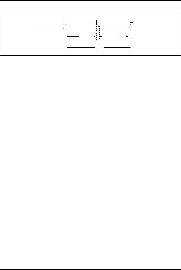
FIGURE 15-5: TIMER0 CLOCK TIMINGS - PIC16C54A
T0CKI
40 |
|
|
|
41 |
|
|
42
Note: Please refer to Figure 15-1 for load conditions.
TABLE 15-4: |
TIMER0 CLOCK REQUIREMENTS - PIC16C54A |
|
|
|
|
|
||||
|
|
Standard Operating Conditions (unless otherwise specified) |
||||||||
|
|
Operating Temperature |
0°C ≤ TA ≤ +70°C for commercial |
|||||||
|
AC Characteristics |
|
–40°C ≤ TA ≤ +85°C for industrial |
|
||||||
|
|
|
|
|
–20°C ≤ TA ≤ +85°C for industrial - PIC16LV54A-02I |
|||||
|
|
|
|
|
–40°C ≤ TA ≤ +125°C for extended |
|
||||
Param |
Symbol |
Characteristic |
|
Min |
Typ† |
Max |
Units |
|
Conditions |
|
No. |
|
|
|
|
|
|
|
|
|
|
|
|
|
|
|
|
|
|
|
|
|
40 |
Tt0H |
T0CKI High Pulse Width |
|
|
|
|
|
|
|
|
|
|
- No Prescaler |
0.5 TCY + 20* |
— |
— |
ns |
|
|
||
|
|
- With Prescaler |
|
|
|
|
|
|
|
|
|
|
|
|
10* |
— |
— |
ns |
|
|
|
|
|
|
|
|
|
|
|
|
|
|
41 |
Tt0L |
T0CKI Low Pulse Width |
|
|
|
|
|
|
|
|
|
|
- No Prescaler |
0.5 TCY + 20* |
— |
— |
ns |
|
|
||
|
|
- With Prescaler |
|
|
|
|
|
|
|
|
|
|
|
|
10* |
— |
— |
ns |
|
|
|
|
|
|
|
|
|
|
|
|||
42 |
Tt0P |
T0CKI Period |
20 or TCY + 40* |
— |
— |
ns |
Whichever is greater. |
|||
|
|
|
|
|
N |
|
|
|
N = |
Prescale Value |
|
|
|
|
|
|
|
|
|
|
(1, 2, 4,..., 256) |
|
|
|
|
|
|
|
|
|
|
|
* These parameters are characterized but not tested.
† Data in the Typical (“Typ”) column is at 5V, 25°C unless otherwise stated. These parameters are for design guidance only and are not tested.
ã 2002 Microchip Technology Inc. |
Preliminary |
DS30453D-page 115

PIC16C5X
NOTES:
DS30453D-page 116 |
Preliminary |
ã 2002 Microchip Technology Inc. |