
- •EPROM-Based 8-Bit CMOS Microcontrollers
- •1.0 General Description
- •1.1 Family and Upward Compatibility
- •1.2 Development Support
- •2.0 PIC16C62X Device Varieties
- •2.1 UV Erasable Devices
- •3.0 Architectural Overview
- •3.1 Clocking Scheme/Instruction Cycle
- •3.2 Instruction Flow/Pipelining
- •4.0 Memory Organization
- •4.1 Program Memory Organization
- •4.2 Data Memory Organization
- •FIGURE 4-4: Data Memory Map for the PIC16C620/621
- •FIGURE 4-5: Data Memory Map for the PIC16C622
- •FIGURE 4-6: Data Memory Map for the PIC16C620A/CR620A/621A
- •FIGURE 4-7: Data Memory Map for the PIC16C622A
- •Register 4-4: PIE1 Register (Address 8Ch)
- •Register 4-5: PIR1 Register (address 0Ch)
- •4.3 PCL and PCLATH
- •FIGURE 4-8: Loading Of PC In Different Situations
- •4.4 Indirect Addressing, INDF and FSR Registers
- •EXAMPLE 4-1: INdirect Addressing
- •5.0 I/O Ports
- •5.1 PORTA and TRISA Registers
- •FIGURE 5-3: Block Diagram of RA3 Pin
- •FIGURE 5-4: Block Diagram of RA4 Pin
- •TABLE 5-2: Summary of Registers Associated with PORTA
- •5.2 PORTB and TRISB Registers
- •FIGURE 5-5: Block Diagram of RB<7:4> Pins
- •FIGURE 5-6: Block Diagram of RB<3:0> Pins
- •5.3 I/O Programming Considerations
- •6.0 Timer0 Module
- •6.1 TIMER0 Interrupt
- •FIGURE 6-2: TIMER0 (TMR0) Timing: Internal Clock/No Prescaler
- •FIGURE 6-3: TIMER0 Timing: Internal Clock/Prescale 1:2
- •FIGURE 6-4: TIMER0 Interrupt Timing
- •6.2 Using Timer0 with External Clock
- •FIGURE 6-5: TIMER0 Timing With External Clock
- •6.3 Prescaler
- •FIGURE 6-6: Block Diagram of thE Timer0/WDT Prescaler
- •7.0 Comparator Module
- •7.1 Comparator Configuration
- •7.2 Comparator Operation
- •7.3 Comparator Reference
- •FIGURE 7-2: Single Comparator
- •7.4 Comparator Response Time
- •7.5 Comparator Outputs
- •FIGURE 7-3: Comparator Output Block Diagram
- •7.6 Comparator Interrupts
- •7.7 Comparator Operation During SLEEP
- •7.8 Effects of a RESET
- •7.9 Analog Input Connection Considerations
- •TABLE 7-1: Registers Associated with Comparator Module
- •8.0 Voltage Reference Module
- •8.1 Configuring the Voltage Reference
- •FIGURE 8-1: Voltage Reference Block Diagram
- •8.2 Voltage Reference Accuracy/Error
- •8.3 Operation During SLEEP
- •8.4 Effects of a RESET
- •8.5 Connection Considerations
- •FIGURE 8-2: Voltage Reference Output Buffer Example
- •TABLE 8-1: Registers Associated with Voltage Reference
- •9.0 Special Features of the CPU
- •9.1 Configuration Bits
- •9.2 Oscillator Configurations
- •FIGURE 9-1: Crystal Operation (or Ceramic Resonator) (HS, XT or LP Osc Configuration)
- •FIGURE 9-2: External Clock Input Operation (HS, XT or LP Osc Configuration)
- •TABLE 9-1: Capacitor Selection for Ceramic Resonators
- •TABLE 9-2: Capacitor Selection for Crystal Oscillator
- •9.3 RESET
- •FIGURE 9-6: Simplified Block Diagram of On-chip Reset Circuit
- •FIGURE 9-7: Brown-out Situations
- •TABLE 9-1: Time-out in Various Situations
- •TABLE 9-3: Summary of Registers Associated with Brown-out
- •TABLE 9-4: Initialization Condition for Special Registers
- •FIGURE 9-8: Time-out Sequence on Power-up (MCLR not tied to Vdd): Case 1
- •FIGURE 9-9: Time-out Sequence on Power-up (MCLR not tied to Vdd): Case 2
- •FIGURE 9-10: Time-out Sequence on Power-up (MCLR tied to Vdd)
- •FIGURE 9-11: External Power-on Reset Circuit (For Slow Vdd Power-up)
- •FIGURE 9-12: External Brown-out Protection Circuit 1
- •FIGURE 9-13: External Brown-out Protection Circuit 2
- •FIGURE 9-14: EXTERNAL BROWN-OUT PROTECTION CIRCUIT 3
- •9.5 Interrupts
- •FIGURE 9-15: Interrupt Logic
- •FIGURE 9-16: INT Pin Interrupt Timing
- •9.6 Context Saving During Interrupts
- •9.7 Watchdog Timer (WDT)
- •FIGURE 9-17: Watchdog Timer Block Diagram
- •TABLE 9-7: Summary of Watchdog Timer Registers
- •9.9 Code Protection
- •9.10 ID Locations
- •FIGURE 9-19: Typical In-Circuit Serial Programming Connection
- •10.0 Instruction Set Summary
- •FIGURE 10-1: General Format for Instructions
- •TABLE 10-2: PIC16C62X Instruction SeT
- •10.1 Instruction Descriptions
- •11.0 Development Support
- •11.1 MPLAB Integrated Development Environment Software
- •11.2 MPASM Assembler
- •11.3 MPLAB C17 and MPLAB C18 C Compilers
- •11.4 MPLINK Object Linker/ MPLIB Object Librarian
- •11.5 MPLAB C30 C Compiler
- •11.6 MPLAB ASM30 Assembler, Linker, and Librarian
- •11.7 MPLAB SIM Software Simulator
- •11.8 MPLAB SIM30 Software Simulator
- •11.11 MPLAB ICD 2 In-Circuit Debugger
- •11.12 PRO MATE II Universal Device Programmer
- •11.13 PICSTART Plus Development Programmer
- •11.14 PICDEM 1 PICmicro Demonstration Board
- •11.15 PICDEM.net Internet/Ethernet Demonstration Board
- •11.16 PICDEM 2 Plus Demonstration Board
- •11.17 PICDEM 3 PIC16C92X Demonstration Board
- •11.19 PICDEM 17 Demonstration Board
- •11.20 PICDEM 18R PIC18C601/801 Demonstration Board
- •11.21 PICDEM LIN PIC16C43X Demonstration Board
- •11.22 PICkitTM 1 FLASH Starter Kit
- •11.23 PICDEM USB PIC16C7X5 Demonstration Board
- •11.24 Evaluation and Programming Tools
- •12.0 Electrical Specifications
- •TABLE 12-1: Comparator Specifications
- •TABLE 12-2: Voltage Reference Specifications
- •12.8 Timing Parameter Symbology
- •FIGURE 12-11: Load Conditions
- •12.9 Timing Diagrams and Specifications
- •FIGURE 12-12: External Clock Timing
- •TABLE 12-3: External Clock Timing Requirements
- •FIGURE 12-13: CLKOUT and I/O Timing
- •TABLE 12-4: CLKOUT and I/O Timing Requirements
- •FIGURE 12-14: Reset, Watchdog Timer, Oscillator Start-Up Timer and Power-Up Timer Timing
- •FIGURE 12-15: Brown-out Reset Timing
- •TABLE 12-5: Reset, Watchdog Timer, Oscillator Start-up Timer and Power-up Timer Requirements
- •FIGURE 12-16: TIMER0 Clock Timing
- •TABLE 12-6: TIMER0 Clock Requirements
- •13.0 Device Characterization Information
- •FIGURE 13-1: Idd vs. Frequency (XT Mode, Vdd = 5.5V)
- •FIGURE 13-2: PIC16C622A Ipd vs. Vdd (WDT Disable)
- •14.0 Packaging Information
- •18-Lead Ceramic Dual In-line with Window (JW) – 300 mil (CERDIP)
- •18-Lead Plastic Dual In-line (P) – 300 mil (PDIP)
- •18-Lead Plastic Small Outline (SO) – Wide, 300 mil (SOIC)
- •20-Lead Plastic Shrink Small Outline (SS) – 209 mil, 5.30 mm (SSOP)
- •14.1 Package Marking Information
- •On-Line Support
- •Systems Information and Upgrade Hot Line
- •Reader Response
- •Product Identification System
- •Worldwide Sales and Service

PIC16C62X
4.3PCL and PCLATH
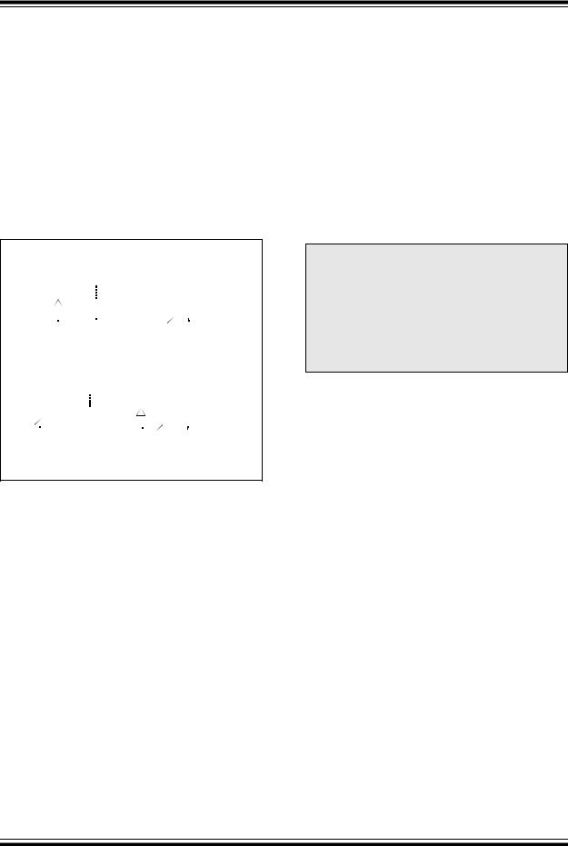
The program counter (PC) is 13-bits wide. The low byte comes from the PCL register, which is a readable and writable register. The high byte (PC<12:8>) is not directly readable or writable and comes from PCLATH. On any RESET, the PC is cleared. Figure 4-8 shows the two situations for the loading of the PC. The upper example in the figure shows how the PC is loaded on a write to PCL (PCLATH<4:0> → PCH). The lower example in the figure shows how the PC is loaded during a CALL or GOTO instruction (PCLATH<4:3> → PCH).
FIGURE 4-8: LOADING OF PC IN DIFFERENT SITUATIONS
|
|
|
|
PCH |
|
|
|
|
|
|
PCL |
|
|
|
||||
12 |
|
|
|
|
|
8 |
7 |
|
|
|
|
0 |
Instruction with |
|||||
|
|
|
|
|
|
|
|
|
|
|
|
|
|
|
|
|
|
|
PC |
|
|
|
|
|
|
|
|
|
|
|
|
|
|
|
|
|
PCL as |
|
|
|
|
|
|
|
PCLATH<4:0> |
|
8 |
Destination |
||||||||
|
|
|
|
|
|
|
|
|
||||||||||
|
|
5 |
|
|
|
|
|
|||||||||||
|
|
|
|
|
|
|
|
|
|
|
|
|
|
|
ALU result |
|||
|
|
|
|
|
|
|
|
|
|
|
|
|
|
|
|
|
|
|
|
|
|
|
|
|
|
|
PCLATH |
|
|
|
|
|
|
||||
|
|
|
PCH |
|
|
|
|
|
|
PCL |
|
|
|
|||||
12 |
11 |
|
10 |
8 |
7 |
|
|
|
|
|
0 |
|
||||||
|
|
|
|
|
|
|
|
|
|
|
|
|
|
|
|
|
GOTO,CALL |
|
PC |
|
|
|
|
|
|
|
|
|
|
|
|
|
|
|
|
|
|
2 |
|
PCLATH<4:3> |
|
|
|
11 |
|
|||||||||||
|
|
|
|
|
||||||||||||||
|
|
|
|
|
|
|
|
|
|
|
|
|
|
|
|
|
|
Opcode <10:0> |
|
|
|
|
|
|
|
|
|
|
|
|
|
|
|
|
|
|
|
|
|
|
|
|
|
|
PCLATH |
|
|
|
|
|
|
4.3.1COMPUTED GOTO
A computed GOTO is accomplished by adding an offset to the program counter (ADDWF PCL). When doing a table read using a computed GOTO method, care should be exercised if the table location crosses a PCL memory boundary (each 256 byte block). Refer to the application note, “Implementing a Table Read"
(AN556).
4.3.2STACK
The PIC16C62X family has an 8-level deep x 13-bit wide hardware stack (Figure 4-2 and Figure 4-3). The stack space is not part of either program or data space and the stack pointer is not readable or writable. The PC is PUSHed onto the stack when a CALL instruction is executed or an interrupt causes a branch. The stack is POPed in the event of a RETURN, RETLW or a RETFIE instruction execution. PCLATH is not affected by a PUSH or POP operation.
The stack operates as a circular buffer. This means that after the stack has been PUSHed eight times, the ninth push overwrites the value that was stored from the first push. The tenth push overwrites the second push (and so on).
Note 1: There are no STATUS bits to indicate stack overflow or stack underflow conditions.
2:There are no instructions/mnemonics called PUSH or POP. These are actions that occur from the execution of the
CALL, RETURN, RETLW and RETFIE instructions, or the vectoring to an interrupt address.
2003 Microchip Technology Inc. |
DS30235J-page 23 |