


PIC16C62X
4.2Data Memory Organization
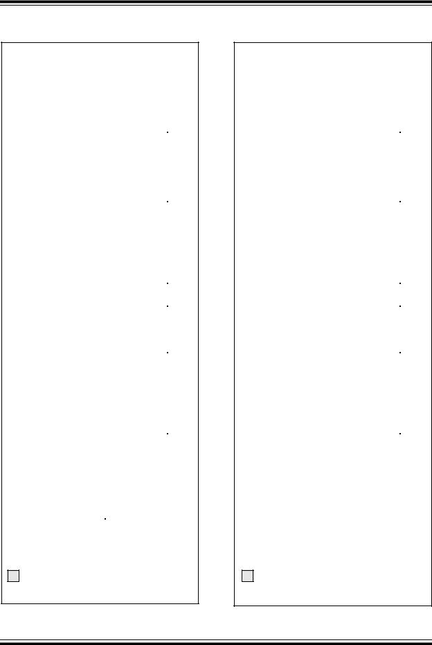
The data memory (Figure 4-4, Figure 4-5, Figure 4-6 and Figure 4-7) is partitioned into two banks, which contain the General Purpose Registers and the Special Function Registers. Bank 0 is selected when the RP0 bit is cleared. Bank 1 is selected when the RP0 bit (STATUS <5>) is set. The Special Function Registers are located in the first 32 locations of each bank. Register locations 20-7Fh (Bank0) on the PIC16C620A/CR620A/621A and 20-7Fh (Bank0) and A0-BFh (Bank1) on the PIC16C622 and PIC16C622A are General Purpose Registers implemented as static RAM. Some Special Purpose Registers are mapped in Bank 1.
Addresses F0h-FFh of bank1 are implemented as common ram and mapped back to addresses 70h-7Fh in bank0 on the PIC16C620A/621A/622A/CR620A.
4.2.1GENERAL PURPOSE REGISTER FILE
The register file is organized as 80 x 8 in the PIC16C620/621, 96 x 8 in the PIC16C620A/621A/ CR620A and 128 x 8 in the PIC16C622(A). Each is accessed either directly or indirectly through the File Select Register FSR (Section 4.4).
DS30235J-page 14 |
2003 Microchip Technology Inc. |

PIC16C62X
FIGURE 4-4: DATA MEMORY MAP FOR THE PIC16C620/621
File |
|
|
|
File |
|||
Address |
|
|
Address |
||||
|
|
|
|
|
|
|
|
00h |
|
INDF(1) |
INDF(1) |
|
80h |
||
01h |
TMR0 |
OPTION |
|
81h |
|||
|
|
|
|
|
|
|
82h |
02h |
|
PCL |
PCL |
|
|||
03h |
STATUS |
STATUS |
|
83h |
|||
|
|
|
|
|
|
|
84h |
04h |
FSR |
FSR |
|
||||
|
|
|
|
|
|
|
85h |
05h |
|
PORTA |
TRISA |
|
|||
06h |
|
PORTB |
TRISB |
|
86h |
||
07h |
|
|
|
|
|
87h |
|
08h |
|
|
|
|
|
88h |
|
09h |
|
|
|
|
|
89h |
|
0Ah |
PCLATH |
PCLATH |
|
8Ah |
|||
|
|
|
|
|
|
8Bh |
|
0Bh |
|
INTCON |
INTCON |
|
|||
0Ch |
|
PIR1 |
PIE1 |
|
8Ch |
||
0Dh |
|
|
|
|
|
8Dh |
|
0Eh |
|
|
|
PCON |
|
8Eh |
|
0Fh |
|
|
|
|
|
8Fh |
|
10h |
|
|
|
|
|
90h |
|
11h |
|
|
|
|
|
91h |
|
12h |
|
|
|
|
|
92h |
|
13h |
|
|
|
|
|
93h |
|
14h |
|
|
|
|
|
94h |
|
15h |
|
|
|
|
|
95h |
|
16h |
|
|
|
|
|
96h |
|
17h |
|
|
|
|
|
97h |
|
18h |
|
|
|
|
|
98h |
|
19h |
|
|
|
|
|
99h |
|
1Ah |
|
|
|
|
|
9Ah |
|
1Bh |
|
|
|
|
|
9Bh |
|
1Ch |
|
|
|
|
|
9Ch |
|
1Dh |
|
|
|
|
|
9Dh |
|
1Eh |
|
|
|
|
|
9Eh |
|
1Fh |
CMCON |
VRCON |
|
9Fh |
|||
|
|
|
|
|
|
|
|
20h |
|
|
|
A0h |
|||
|
|
|
|
General |
|
|
|
|
|
|
|
|
|
|
|
|
|
|
|
Purpose |
|
|
|
6Fh |
|
Register |
|
|
|
||
|
|
|
|
||||
70h |
|
|
|
|
|||
|
|
|
|
|
|
|
|
|
|
|
|
|
|
|
|
7Fh |
|
|
FFh |
|
|
||
|
Bank 0 |
Bank 1 |
|
Unimplemented data memory locations, read as '0'.
Note 1: Not a physical register.
FIGURE 4-5: DATA MEMORY MAP FOR THE PIC16C622
File |
|
|
|
File |
|||
Address |
|
|
Address |
||||
|
|
|
|
|
|
|
|
00h |
|
INDF(1) |
INDF(1) |
|
80h |
||
01h |
TMR0 |
OPTION |
|
81h |
|||
|
|
|
|
|
|
|
82h |
02h |
|
PCL |
PCL |
|
|||
03h |
STATUS |
STATUS |
|
83h |
|||
|
|
|
|
|
|
|
84h |
04h |
FSR |
FSR |
|
||||
|
|
|
|
|
|
|
85h |
05h |
|
PORTA |
TRISA |
|
|||
06h |
|
PORTB |
TRISB |
|
86h |
||
07h |
|
|
|
|
|
87h |
|
08h |
|
|
|
|
|
88h |
|
09h |
|
|
|
|
|
89h |
|
0Ah |
PCLATH |
PCLATH |
|
8Ah |
|||
|
|
|
|
|
|
8Bh |
|
0Bh |
|
INTCON |
INTCON |
|
|||
0Ch |
|
PIR1 |
PIE1 |
|
8Ch |
||
0Dh |
|
|
|
|
|
8Dh |
|
0Eh |
|
|
|
PCON |
|
8Eh |
|
0Fh |
|
|
|
|
|
8Fh |
|
10h |
|
|
|
|
|
90h |
|
11h |
|
|
|
|
|
91h |
|
12h |
|
|
|
|
|
92h |
|
13h |
|
|
|
|
|
93h |
|
14h |
|
|
|
|
|
94h |
|
15h |
|
|
|
|
|
95h |
|
16h |
|
|
|
|
|
96h |
|
17h |
|
|
|
|
|
97h |
|
18h |
|
|
|
|
|
98h |
|
19h |
|
|
|
|
|
99h |
|
1Ah |
|
|
|
|
|
9Ah |
|
1Bh |
|
|
|
|
|
9Bh |
|
1Ch |
|
|
|
|
|
9Ch |
|
1Dh |
|
|
|
|
|
9Dh |
|
1Eh |
|
|
|
|
|
9Eh |
|
1Fh |
CMCON |
VRCON |
|
9Fh |
|||
|
|
|
|
|
|
|
|
20h |
|
|
|
A0h |
|||
|
|
|
|
General |
General |
|
|
|
|
|
|
|
|
||
|
|
|
|
Purpose |
Purpose |
|
|
|
|
|
|
Register |
Register |
|
BFh |
|
|
|
|
|
|
|
|
|
|
|
|
|
|
|
C0h |
|
|
|
|
|
|
|
|
|
|
|
|
|
|
|
|
7Fh |
|
|
FFh |
|
|
||
|
Bank 0 |
Bank 1 |
|
Unimplemented data memory locations, read as '0'.
Note 1: Not a physical register.
2003 Microchip Technology Inc. |
DS30235J-page 15 |
PIC16C62X
FIGURE 4-6: DATA MEMORY MAP FOR THE PIC16C620A/CR620A/621A
File |
|
|
File |
|
Address |
|
|
Address |
|
|
|
|
|
|
00h |
|
INDF(1) |
INDF(1) |
80h |
01h |
|
TMR0 |
OPTION |
81h |
02h |
|
|
|
82h |
|
PCL |
PCL |
||
03h |
|
STATUS |
STATUS |
83h |
04h |
|
|
|
84h |
|
FSR |
FSR |
||
05h |
|
|
|
85h |
|
PORTA |
TRISA |
||
06h |
|
PORTB |
TRISB |
86h |
07h |
|
|
|
87h |
08h |
|
|
|
88h |
09h |
|
|
|
89h |
0Ah |
|
PCLATH |
PCLATH |
8Ah |
0Bh |
|
INTCON |
INTCON |
8Bh |
0Ch |
|
PIR1 |
PIE1 |
8Ch |
0Dh |
|
|
|
8Dh |
0Eh |
|
|
PCON |
8Eh |
0Fh |
|
|
|
8Fh |
10h |
|
|
|
90h |
11h |
|
|
|
91h |
12h |
|
|
|
92h |
13h |
|
|
|
93h |
14h |
|
|
|
94h |
15h |
|
|
|
95h |
16h |
|
|
|
96h |
17h |
|
|
|
97h |
18h |
|
|
|
98h |
19h |
|
|
|
99h |
1Ah |
|
|
|
9Ah |
1Bh |
|
|
|
9Bh |
1Ch |
|
|
|
9Ch |
1Dh |
|
|
|
9Dh |
1Eh |
|
|
|
9Eh |
1Fh |
|
CMCON |
VRCON |
9Fh |
20h |
|
|
|
A0h |
|
|
|
||
|
|
General |
|
|
|
|
|
|
|
|
|
Purpose |
|
|
|
|
Register |
|
|
6Fh |
|
|
|
|
|
|
|
|
F0h |
70h |
|
General |
Accesses |
|
|
|
|||
|
|
Purpose |
|
|
|
|
70h-7Fh |
|
|
|
|
Register |
|
|
7Fh |
|
|
FFh |
|
|
|
|
||
|
Bank 0 |
Bank 1 |
||
|
|
|
||
Unimplemented data memory locations, read as '0'.
Note 1: Not a physical register.
FIGURE 4-7: DATA MEMORY MAP FOR THE PIC16C622A
File |
|
|
File |
|
Address |
|
|
Address |
|
|
|
|
|
|
00h |
|
INDF(1) |
INDF(1) |
80h |
01h |
|
TMR0 |
OPTION |
81h |
02h |
|
|
|
82h |
|
PCL |
PCL |
||
03h |
|
STATUS |
STATUS |
83h |
04h |
|
|
|
84h |
|
FSR |
FSR |
||
05h |
|
|
|
85h |
|
PORTA |
TRISA |
||
06h |
|
PORTB |
TRISB |
86h |
07h |
|
|
|
87h |
08h |
|
|
|
88h |
09h |
|
|
|
89h |
0Ah |
|
PCLATH |
PCLATH |
8Ah |
0Bh |
|
INTCON |
INTCON |
8Bh |
0Ch |
|
PIR1 |
PIE1 |
8Ch |
0Dh |
|
|
|
8Dh |
0Eh |
|
|
PCON |
8Eh |
0Fh |
|
|
|
8Fh |
10h |
|
|
|
90h |
11h |
|
|
|
91h |
12h |
|
|
|
92h |
13h |
|
|
|
93h |
14h |
|
|
|
94h |
15h |
|
|
|
95h |
16h |
|
|
|
96h |
17h |
|
|
|
97h |
18h |
|
|
|
98h |
19h |
|
|
|
99h |
1Ah |
|
|
|
9Ah |
1Bh |
|
|
|
9Bh |
1Ch |
|
|
|
9Ch |
1Dh |
|
|
|
9Dh |
1Eh |
|
|
|
9Eh |
1Fh |
|
CMCON |
VRCON |
9Fh |
20h |
|
|
|
A0h |
|
|
|
||
|
|
General |
General |
|
|
|
|
||
|
|
Purpose |
Purpose |
|
|
|
Register |
Register |
BFh |
|
|
|
|
|
|
|
|
|
C0h |
6Fh |
|
|
|
F0h |
70h |
|
General |
Accesses |
|
|
|
|||
|
|
Purpose |
|
|
|
|
70h-7Fh |
|
|
|
|
Register |
|
|
7Fh |
|
|
FFh |
|
|
|
|
||
|
Bank 0 |
Bank 1 |
||
|
|
|
||
Unimplemented data memory locations, read as '0'.
Note 1: Not a physical register.
DS30235J-page 16 |
2003 Microchip Technology Inc. |

PIC16C62X
4.2.2SPECIAL FUNCTION REGISTERS
The Special Function Registers are registers used by the CPU and Peripheral functions for controlling the desired operation of the device (Table 4-1). These registers are static RAM.
The Special Function Registers can be classified into two sets (core and peripheral). The Special Function Registers associated with the “core” functions are described in this section. Those related to the operation of the peripheral features are described in the section of that peripheral feature.
TABLE 4-1: |
SPECIAL REGISTERS FOR THE PIC16C62X |
|
|
|
|
|
|
|
|
|
|
||||||||||||||||||||
|
|
|
|
|
|
|
|
|
|
|
|
|
|
|
|
|
|
|
|
|
|
|
|
|
|
|
|
|
|
|
|
|
|
|
|
|
|
|
|
|
|
|
|
|
|
|
|
|
|
|
|
|
|
|
|
|
|
|
|
Value on |
Value on all |
||
Address |
Name |
|
|
Bit 7 |
Bit 6 |
Bit 5 |
Bit 4 |
|
Bit 3 |
Bit 2 |
|
Bit 1 |
|
Bit 0 |
other |
||||||||||||||||
|
|
|
|
|
POR Reset |
||||||||||||||||||||||||||
|
|
|
|
|
|
|
|
|
|
|
|
|
|
|
|
|
|
|
|
|
|
|
|
|
|
|
|
RESETS(1) |
|||
|
|
|
|
|
|
|
|
|
|
|
|
|
|
|
|
|
|
|
|
|
|
|
|
|
|
|
|
|
|
||
|
|
|
|
|
|
|
|
|
|
|
|
|
|
|
|
|
|
|
|
|
|
|
|
|
|
|
|
|
|
|
|
Bank 0 |
|
|
|
|
|
|
|
|
|
|
|
|
|
|
|
|
|
|
|
|
|
|
|
|
|
|
|
|
|
|
|
|
|
|
|
|
|
||||||||||||||||||||||||||
00h |
INDF |
|
Addressing this location uses contents of FSR to address data memory (not a physical |
xxxx xxxx |
xxxx xxxx |
||||||||||||||||||||||||||
|
|
|
register) |
|
|
|
|
|
|
|
|
|
|
|
|
|
|
|
|
|
|
|
|
|
|
|
|
|
|
||
01h |
TMR0 |
|
Timer0 Module’s Register |
|
|
|
|
|
|
|
|
|
|
|
|
|
|
|
|
|
|
|
|
xxxx xxxx |
uuuu uuuu |
||||||
02h |
PCL |
|
Program Counter's (PC) Least Significant Byte |
|
|
|
|
|
|
|
|
|
|
|
|
|
|
0000 0000 |
0000 0000 |
||||||||||||
03h |
STATUS |
|
|
IRP(2) |
RP1(2) |
RP0 |
|
|
TO |
|
|
PD |
|
Z |
|
DC |
|
C |
0001 |
1xxx |
000q |
quuu |
|||||||||
04h |
FSR |
|
Indirect data memory address pointer |
|
|
|
|
|
|
|
|
|
|
|
|
|
|
xxxx xxxx |
uuuu uuuu |
||||||||||||
|
|
|
|
|
|
|
|
|
|
|
|
|
|
|
|
|
|
|
|
|
|
|
|
|
|
||||||
05h |
PORTA |
|
|
— |
— |
— |
RA4 |
|
RA3 |
|
RA2 |
|
RA1 |
|
RA0 |
---x 0000 |
---u 0000 |
||||||||||||||
|
|
|
|
|
|
|
|
|
|
|
|
|
|
|
|
|
|
|
|
|
|
|
|
|
|
|
|
|
|
|
|
06h |
PORTB |
|
|
RB7 |
RB6 |
RB5 |
RB4 |
|
RB3 |
|
RB2 |
|
RB1 |
|
RB0 |
xxxx xxxx |
uuuu uuuu |
||||||||||||||
07h-09h |
Unimplemented |
|
|
|
|
|
|
|
|
|
|
|
|
|
|
|
|
|
|
|
|
|
|
|
|
|
— |
— |
|||
0Ah |
PCLATH |
|
|
— |
— |
— |
Write buffer for upper 5 bits of program counter |
---0 0000 |
---0 0000 |
||||||||||||||||||||||
0Bh |
INTCON |
|
|
GIE |
PEIE |
T0IE |
INTE |
|
RBIE |
T0IF |
INTF |
RBIF |
0000 |
000x |
0000 |
000u |
|||||||||||||||
0Ch |
PIR1 |
|
|
— |
CMIF |
— |
|
|
— |
|
|
|
— |
|
— |
|
— |
|
— |
-0-- ---- |
-0-- ---- |
||||||||||
0Dh-1Eh |
Unimplemented |
|
|
|
|
|
|
|
|
|
|
|
|
|
|
|
|
|
|
|
|
|
|
|
|
|
— |
— |
|||
1Fh |
CMCON |
|
C2OUT |
C1OUT |
— |
|
|
— |
|
|
CIS |
CM2 |
|
CM1 |
|
CM0 |
00-- 0000 |
00-- 0000 |
|||||||||||||
Bank 1 |
|
|
|
|
|
|
|
|
|
|
|
|
|
|
|
|
|
|
|
|
|
|
|
|
|
|
|
|
|
|
|
|
|
|
|
|
|
|
|
||||||||||||||||||||||||
80h |
INDF |
|
Addressing this location uses contents of FSR to address data memory (not a physical |
xxxx xxxx |
xxxx xxxx |
||||||||||||||||||||||||||
|
|
|
register) |
|
|
|
|
|
|
|
|
|
|
|
|
|
|
|
|
|
|
|
|
|
|
||||||
|
|
|
|
|
|
|
|
|
|
|
|
|
|
|
|
|
|
|
|
|
|
|
|
|
|
|
|
|
|||
81h |
OPTION |
|
|
RBPU |
INTEDG |
T0CS |
T0SE |
|
PSA |
|
PS2 |
|
PS1 |
|
PS0 |
1111 1111 |
1111 1111 |
||||||||||||||
82h |
PCL |
|
Program Counter's (PC) Least Significant Byte |
|
|
|
|
|
|
|
|
|
|
|
|
|
|
0000 0000 |
0000 0000 |
||||||||||||
83h |
STATUS |
|
|
IRP(2) |
RP1(2) |
RP0 |
|
|
TO |
|
|
PD |
|
Z |
|
DC |
|
C |
0001 1xxx |
000q quuu |
|||||||||||
84h |
FSR |
|
Indirect data memory address pointer |
|
|
|
|
|
|
|
|
|
|
|
|
|
|
xxxx xxxx |
uuuu uuuu |
||||||||||||
85h |
TRISA |
|
|
— |
— |
— |
TRISA4 |
TRISA3 |
TRISA2 |
TRISA1 |
TRISA0 |
---1 1111 |
---1 1111 |
||||||||||||||||||
86h |
TRISB |
|
TRISB7 |
TRISB6 |
TRISB5 |
TRISB4 |
TRISB3 |
TRISB2 |
TRISB1 |
TRISB0 |
1111 1111 |
1111 1111 |
|||||||||||||||||||
87h-89h |
Unimplemented |
|
|
|
|
|
|
|
|
|
|
|
|
|
|
|
|
|
|
|
|
|
|
|
|
|
— |
— |
|||
8Ah |
PCLATH |
|
|
— |
— |
— |
Write buffer for upper 5 bits of program counter |
---0 0000 |
---0 0000 |
||||||||||||||||||||||
8Bh |
INTCON |
|
|
GIE |
PEIE |
T0IE |
INTE |
|
RBIE |
T0IF |
INTF |
RBIF |
0000 000x |
0000 000u |
|||||||||||||||||
8Ch |
PIE1 |
|
|
— |
CMIE |
— |
|
|
— |
|
|
|
— |
|
— |
|
— |
|
— |
-0-- ---- |
-0-- ---- |
||||||||||
8Dh |
Unimplemented |
|
|
|
|
|
|
|
|
|
|
|
|
|
|
|
|
|
|
|
|
|
|
|
|
|
— |
— |
|||
8Eh |
PCON |
|
|
— |
— |
— |
|
|
— |
|
|
|
— |
|
— |
|
POR |
|
BOR |
---- --0x |
---- --uq |
||||||||||
8Fh-9Eh |
Unimplemented |
|
|
|
|
|
|
|
|
|
|
|
|
|
|
|
|
|
|
|
|
|
|
|
|
|
— |
— |
|||
9Fh |
VRCON |
|
|
VREN |
VROE |
VRR |
|
|
— |
|
VR3 |
|
VR2 |
|
VR1 |
|
VR0 |
0000000 |
0000000 |
||||||||||||
Legend: — = Unimplemented locations read as ‘0’, u = unchanged, x = unknown, q = value depends on condition, shaded = unimplemented
Note 1: Other (non Power-up) Resets include MCLR Reset, Brown-out Reset and Watchdog Timer Reset during normal operation.
2: IRP & RP1 bits are reserved; always maintain these bits clear.
2003 Microchip Technology Inc. |
DS30235J-page 17 |

PIC16C62X
4.2.2.1STATUS Register
The STATUS register, shown in Register 4-1, contains the arithmetic status of the ALU, the RESET status and the bank select bits for data memory.
The STATUS register can be the destination for any instruction, like any other register. If the STATUS register is the destination for an instruction that affects the Z, DC or C bits, then the write to these three bits is disabled. These bits are set or cleared according to the device logic. Furthermore, the TO and PD bits are not writable. Therefore, the result of an instruction with the STATUS register as destination may be different than intended.
For example, CLRF STATUS will clear the upper-three bits and set the Z bit. This leaves the STATUS register as 000uu1uu (where u = unchanged).
It is recommended, therefore, that only BCF, BSF, SWAPF and MOVWF instructions are used to alter the STATUS register, because these instructions do not affect any STATUS bit. For other instructions not affecting any STATUS bits, see the “Instruction Set Summary”.
Note 1: The IRP and RP1 bits (STATUS<7:6>) are not used by the PIC16C62X and should be programmed as ’0'. Use of these bits as general purpose R/W bits is NOT recommended, since this may affect upward compatibility with future products.
2:The C and DC bits operate as a Borrow and Digit Borrow out bit, respectively, in subtraction. See the SUBLW and SUBWF instructions for examples.
REGISTER 4-1: |
STATUS REGISTER (ADDRESS 03H OR 83H) |
|
|
|
||||||||||||
|
Reserved |
Reserved |
R/W-0 |
R-1 |
R-1 |
R/W-x |
R/W-x |
R/W-x |
||||||||
|
|
|
|
|
|
|
|
|
|
|
|
|
|
|
|
|
|
|
|
|
|
|
|
|
|
|
|
|
|
|
|
|
|
|
IRP |
|
|
RP1 |
|
RP0 |
|
TO |
PD |
|
Z |
DC |
C |
|||
|
bit 7 |
|
|
|
|
|
|
|
|
|
|
|
|
|
bit 0 |
|
bit 7 |
IRP: Register Bank Select bit (used for indirect addressing) |
|
|
|
||||||||||||
|
1 = Bank 2, |
3 |
(100h - 1FFh) |
|
|
|
|
|
|
|
|
|
|
|||
|
0 = Bank 0, |
1 |
(00h - FFh) |
|
|
|
|
|
|
|
|
|
|
|
||
The IRP bit is reserved on the PIC16C62X; always maintain this bit clear.
bit 6-5 |
RP<1:0>: Register Bank Select bits (used for direct addressing) |
||||||||
|
01 = Bank 1 (80h - FFh) |
||||||||
|
00 = Bank 0 (00h - 7Fh) |
||||||||
|
Each bank is 128 bytes. The RP1 bit is reserved on the PIC16C62X; always maintain this bit |
||||||||
|
clear. |
||||||||
|
|
|
|
|
|
|
|
|
|
bit 4 |
TO: Time-out bit |
||||||||
|
1 |
= After power-up, CLRWDT instruction, or SLEEP instruction |
|||||||
|
0 |
= A WDT time-out occurred |
|||||||
|
|
|
|
|
|
|
|
|
|
bit 3 |
PD: Power-down bit |
||||||||
|
1 |
= After power-up or by the CLRWDT instruction |
|||||||
|
0 |
= By execution of the SLEEP instruction |
|||||||
bit 2 |
Z: Zero bit |
||||||||
|
1 |
= The result of an arithmetic or logic operation is zero |
|||||||
|
0 |
= The result of an arithmetic or logic operation is not zero |
|||||||
|
|
|
|
|
|
|
|
||
bit 1 |
DC: Digit carry/borrow bit (ADDWF, ADDLW,SUBLW,SUBWF instructions)(for borrow the polarity |
||||||||
|
is reversed) |
||||||||
|
1 |
= A carry-out from the 4th low order bit of the result occurred |
|||||||
|
0 |
= No carry-out from the 4th low order bit of the result |
|||||||
|
|
|
|
||||||
bit 0 |
C: Carry/borrow bit (ADDWF, ADDLW,SUBLW,SUBWF instructions) |
||||||||
|
1 |
= A carry-out from the Most Significant bit of the result occurred |
|||||||
|
0 |
= No carry-out from the Most Significant bit of the result occurred |
|||||||
Note: For borrow the polarity is reversed. A subtraction is executed by adding the two’s complement of the second operand. For rotate (RRF, RLF) instructions, this bit is loaded with either the high or low order bit of the source register.
|
Legend: |
|
|
|
|
R = Readable bit |
W = Writable bit |
U = Unimplemented bit, read as ‘0’ |
|
|
- n = Value at POR |
’1’ = Bit is set |
’0’ = Bit is cleared |
x = Bit is unknown |
|
|
|
|
|
|
|
|
|
|
|
|
|
|
|
|
|
|
|
|
DS30235J-page 18 |
2003 Microchip Technology Inc. |
PIC16C62X
4.2.2.2OPTION Register
The OPTION register is a readable and writable |
Note: To achieve a 1:1 prescaler assignment for |
|
TMR0, assign the prescaler to the WDT |
||
register, which contains various control bits to configure |
||
(PSA = 1). |
||
the TMR0/WDT prescaler, the external RB0/INT |
||
|
||
interrupt, TMR0 and the weak pull-ups on PORTB. |
|
REGISTER 4-2: |
OPTION REGISTER (ADDRESS 81H) |
|
|
|
|
|
|||||||||||||||
|
|
|
R/W-1 |
|
R/W-1 |
|
|
R/W-1 |
|
|
R/W-1 |
R/W-1 |
R/W-1 |
R/W-1 |
R/W-1 |
||||||
|
|
|
|
|
|
|
|
|
|
|
|
|
|
|
|
|
|
|
|
|
|
|
|
|
RBPU |
|
INTEDG |
|
|
T0CS |
|
|
T0SE |
|
PSA |
PS2 |
PS1 |
|
PS0 |
||||
|
|
|
|
|
|
|
|
|
|
|
|
|
|
|
|
|
|
|
|||
|
bit 7 |
|
|
|
|
|
|
|
|
|
|
|
|
|
|
|
|
bit 0 |
|||
|
|
|
|
|
|
|
|
|
|
|
|
|
|
|
|
|
|||||
bit 7 |
|
RBPU: PORTB Pull-up Enable bit |
|
|
|
|
|
|
|
|
|||||||||||
|
1 |
= PORTB pull-ups are disabled |
|
|
|
|
|
|
|
|
|
|
|||||||||
|
0 |
= PORTB pull-ups are enabled by individual port latch values |
|
|
|
||||||||||||||||
bit 6 |
|
INTEDG: Interrupt Edge Select bit |
|
|
|
|
|
|
|
|
|
|
|||||||||
|
1 |
= Interrupt on rising edge of RB0/INT pin |
|
|
|
|
|
||||||||||||||
|
0 |
= Interrupt on falling edge of RB0/INT pin |
|
|
|
|
|
||||||||||||||
bit 5 |
|
T0CS: TMR0 Clock Source Select bit |
|
|
|
|
|
|
|
|
|||||||||||
|
1 |
= Transition on RA4/T0CKI pin |
|
|
|
|
|
|
|
|
|
|
|||||||||
|
0 |
= Internal instruction cycle clock (CLKOUT) |
|
|
|
|
|
||||||||||||||
bit 4 |
|
T0SE: TMR0 Source Edge Select bit |
|
|
|
|
|
|
|
|
|||||||||||
|
1 |
= Increment on high-to-low transition on RA4/T0CKI pin |
|
|
|
|
|||||||||||||||
|
0 |
= Increment on low-to-high transition on RA4/T0CKI pin |
|
|
|
|
|||||||||||||||
bit 3 |
|
PSA: Prescaler Assignment bit |
|
|
|
|
|
|
|
|
|
|
|||||||||
|
1 |
= Prescaler is assigned to the WDT |
|
|
|
|
|
|
|
|
|||||||||||
|
0 |
= Prescaler is assigned to the Timer0 module |
|
|
|
|
|
||||||||||||||
bit 2-0 |
|
PS<2:0>: Prescaler Rate Select bits |
|
|
|
|
|
|
|
|
|||||||||||
|
|
|
|
|
Bit Value |
TMR0 Rate |
WDT Rate |
|
|
|
|
|
|||||||||
|
|
|
|
|
|
|
|
|
|
|
|
|
|
|
|
|
|
|
|||
|
|
|
|
|
000 |
|
1 |
: 2 |
|
1 |
: 1 |
|
|
|
|
|
|
|
|||
|
|
|
|
|
001 |
|
1 |
: 4 |
|
1 |
: 2 |
|
|
|
|
|
|
|
|||
|
|
|
|
|
010 |
|
1 |
: 8 |
|
1 |
: 4 |
|
|
|
|
|
|
|
|||
|
|
|
|
|
011 |
|
1 |
: 16 |
|
1 |
: 8 |
|
|
|
|
|
|
|
|||
|
|
|
|
|
100 |
|
1 |
: 32 |
|
1 |
: 16 |
|
|
|
|
|
|
|
|||
|
|
|
|
|
101 |
|
1 |
: 64 |
|
1 |
: 32 |
|
|
|
|
|
|
|
|||
|
|
|
|
|
110 |
|
1 |
: 128 |
|
1 |
: 64 |
|
|
|
|
|
|
|
|||
|
|
|
|
|
111 |
|
1 |
: 256 |
|
1 |
: 128 |
|
|
|
|
|
|
|
|||
|
|
|
|
|
|
|
|
|
|
|
|
|
|
|
|
|
|
|
|
|
|
|
|
Legend: |
|
|
|
|
|
|
|
|
|
|
|
|
|
|
|
|
|
||
|
|
R = Readable bit |
|
|
W = Writable bit |
U = Unimplemented bit, read as ‘0’ |
|
||||||||||||||
|
|
- n = Value at POR |
|
|
’1’ = Bit is set |
’0’ = Bit is cleared |
x = Bit is unknown |
||||||||||||||
|
|
|
|
|
|
|
|
|
|
|
|
|
|
|
|
|
|
|
|
|
|
2003 Microchip Technology Inc. |
DS30235J-page 19 |

PIC16C62X
4.2.2.3INTCON Register
The INTCON register is a readable and writable |
Note: Interrupt flag bits get set when an interrupt |
|
condition occurs, regardless of the state of |
||
register, which contains the various enable and flag bits |
||
its corresponding enable bit or the global |
||
for all interrupt sources except the comparator module. |
||
enable bit, GIE (INTCON<7>). |
||
See Section 4.2.2.4 and Section 4.2.2.5 for a |
||
|
||
description of the comparator enable and flag bits. |
|
REGISTER 4-3: |
INTCON REGISTER (ADDRESS 0BH OR 8BH) |
|
|
|
|
||||||||
|
|
R/W-0 |
R/W-0 |
R/W-0 |
R/W-0 |
R/W-0 |
R/W-0 |
R/W-0 |
R/W-x |
||||
|
|
|
|
|
|
|
|
|
|
|
|
|
|
|
|
GIE |
PEIE |
|
T0IE |
|
INTE |
|
RBIE |
T0IF |
INTF |
|
RBIF |
|
|
|
|
|
|
|
|
|
|
|
|
|
|
|
bit 7 |
|
|
|
|
|
|
|
|
|
|
bit 0 |
|
bit 7 |
GIE: Global Interrupt Enable bit |
|
|
|
|
|
|
|
|||||
|
1 |
= Enables all un-masked interrupts |
|
|
|
|
|
|
|
||||
|
0 |
= Disables all interrupts |
|
|
|
|
|
|
|
|
|
||
bit 6 |
PEIE: Peripheral Interrupt Enable bit |
|
|
|
|
|
|
|
|||||
|
1 |
= Enables all un-masked peripheral interrupts |
|
|
|
|
|
||||||
|
0 |
= Disables all peripheral interrupts |
|
|
|
|
|
|
|
||||
bit 5 |
T0IE: TMR0 Overflow Interrupt Enable bit |
|
|
|
|
|
|||||||
|
1 |
= Enables the TMR0 interrupt |
|
|
|
|
|
|
|
||||
|
0 |
= Disables the TMR0 interrupt |
|
|
|
|
|
|
|
||||
bit 4 |
INTE: RB0/INT External Interrupt Enable bit |
|
|
|
|
|
|||||||
|
1 |
= Enables the RB0/INT external interrupt |
|
|
|
|
|
||||||
|
0 |
= Disables the RB0/INT external interrupt |
|
|
|
|
|
||||||
bit 3 |
RBIE: RB Port Change Interrupt Enable bit |
|
|
|
|
|
|||||||
|
1 |
= Enables the RB port change interrupt |
|
|
|
|
|
||||||
|
0 |
= Disables the RB port change interrupt |
|
|
|
|
|
||||||
bit 2 |
T0IF: TMR0 Overflow Interrupt Flag bit |
|
|
|
|
|
|||||||
|
1 |
= TMR0 register has overflowed (must be cleared in software) |
|
|
|
||||||||
|
0 |
= TMR0 register did not overflow |
|
|
|
|
|
|
|
||||
bit 1 |
INTF: RB0/INT External Interrupt Flag bit |
|
|
|
|
|
|||||||
|
1 |
= The RB0/INT external interrupt occurred (must be cleared in software) |
|
||||||||||
|
0 |
= The RB0/INT external interrupt did not occur |
|
|
|
|
|
||||||
bit 0 |
RBIF: RB Port Change Interrupt Flag bit |
|
|
|
|
|
|||||||
|
1 |
= When at least one of the RB<7:4> pins changed state (must be cleared in software) |
|||||||||||
|
0 |
= None of the RB<7:4> pins have changed state |
|
|
|
|
|||||||
|
|
|
|
|
|
|
|
|
|
|
|
|
|
|
Legend: |
|
|
|
|
|
|
|
|
|
|
|
|
|
R = Readable bit |
W = Writable bit |
U = Unimplemented bit, read as ‘0’ |
|
|||||||||
|
- n = Value at POR |
’1’ = Bit is set |
’0’ = Bit is cleared |
x = Bit is unknown |
|||||||||
|
|
|
|
|
|
|
|
|
|
|
|
|
|
DS30235J-page 20 |
2003 Microchip Technology Inc. |