

PIC16C62X
4.4Indirect Addressing, INDF and FSR Registers
The INDF register is not a physical register. Addressing the INDF register will cause indirect addressing.
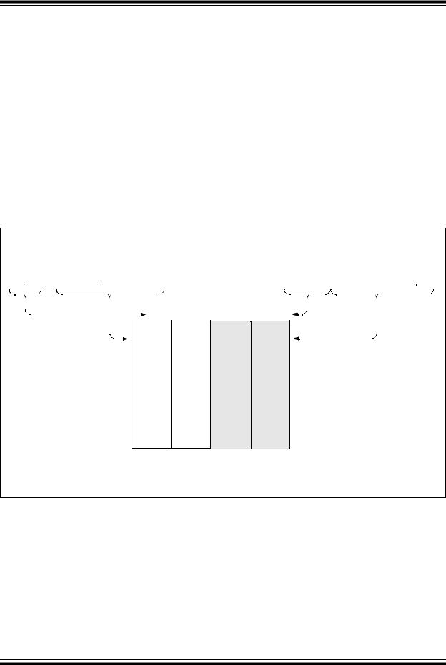
Indirect addressing is possible by using the INDF register. Any instruction using the INDF register actually accesses data pointed to by the File Select Register (FSR). Reading INDF itself indirectly will produce 00h. Writing to the INDF register indirectly results in a no-operation (although STATUS bits may be affected). An effective 9-bit address is obtained by concatenating the 8-bit FSR register and the IRP bit (STATUS<7>), as shown in Figure 4-9. However, IRP is not used in the PIC16C62X.
A simple program to clear RAM location 20h-7Fh using indirect addressing is shown in Example 4-1.
EXAMPLE 4-1: INDIRECT ADDRESSING
movlw |
0x20 |
;initialize pointer |
movwf |
FSR |
;to RAM |
NEXT clrf |
INDF |
;clear INDF register |
incf |
FSR |
;inc pointer |
btfss |
FSR,7 |
;all done? |
goto |
NEXT |
;no clear next |
|
|
;yes continue |
CONTINUE: |
|
|
|
|
|
FIGURE 4-9: |
|
DIRECT/INDIRECT ADDRESSING PIC16C62X |
|
|
|
|
|
|
|
|
|
|||||||||||||||||||||||
|
|
|
|
|
|
|
|
|
|
|
|
|
|
|
|
|
|
|
||||||||||||||||
|
|
|
|
|
|
Direct Addressing |
|
|
|
|
|
|
|
|
|
Indirect Addressing |
|
|
||||||||||||||||
RP1 RP0(1) |
6 |
from opcode |
0 |
|
|
|
IRP(1) 7 |
|
FSR register |
0 |
|
|||||||||||||||||||||||
|
|
|
|
|
|
|
|
|
|
|
|
|
|
|
|
|
|
|
|
|
|
|
|
|
|
|
|
|
|
|
|
|
|
|
|
|
|
|
|
|
|
|
|
|
|
|
|
|
|
|
|
|
|
|
|
|
|
|
|
|
|
|
|||||||
bank select |
location select |
|
|
|
00 |
01 |
10 |
11 |
bank select |
|
|
|
|
location select |
|
|||||||||||||||||||
|
|
|
|
|
|
|
|
|||||||||||||||||||||||||||
|
|
|
|
|
|
|
|
|
|
|
|
|
|
|
|
|
|
|
|
|
|
|
|
|
|
|
|
|
|
|
||||
|
|
|
|
|
|
|
|
|
|
|
00h |
|
|
|
180h |
|
|
|
|
|
|
|
|
|
||||||||||
|
|
|
|
|
|
|
|
|
|
|
|
|
|
|
|
|
|
|
|
|
|
|
|
|
|
|
||||||||
|
|
|
|
|
|
|
|
|
|
|
|
|
|
|
|
|
|
|
|
|
|
|
||||||||||||
|
|
|
|
|
|
|
|
|
|
|
|
|
|
|
|
|
|
|
|
|
|
|
|
|
|
|
|
|
|
|
|
|
|
|
|
|
|
|
|
|
|
|
|
|
|
|
|
|
|
|
|
|
|
|
|
|
|
|
|
|
|
|
|
|
|
|
|
|
|
not used
Data Memory
7Fh |
1FFh |
|
Bank 0 Bank 1 Bank 2 Bank 3
For memory map detail see (Figure 4-4, Figure 4-5, Figure 4-6 and Figure 4-7).
Note 1: The RP1 and IRP bits are reserved; always maintain these bits clear.
DS30235J-page 24 |
2003 Microchip Technology Inc. |