

СПП1 / СППП. РГЗ / Паспортные данные MOSFET / APT30M30LLL
.pdfAPT30M30B2LL
APT30M30LLL
300V 100A 0.030Ω
POWER MOS 7 |
R |
MOSFET |
B2LL |
|
|
||
|
|
|
Power MOS 7® is a new generation of low loss, high voltage, N-Channel enhancement mode power MOSFETS. Both conduction and switching
losses are addressed with Power MOS 7® by significantly lowering RDS(ON) and Qg. Power MOS 7® combines lower conduction and switching losses
along with exceptionally fast switching speeds inherent with APT's patented metal gate structure.
T-MAX™ TO-264
LLL
• Lower Input Capacitance |
• Increased Power Dissipation |
|
|
|
|
|
|
|
|
|
|
|
|
D |
|
|
|
|
|
|
|
|
|
|
|
|
|||||
|
|
|
|
|
|
|
|
|
|
|
|
|
|||
• Lower Miller Capacitance |
• Easier To Drive |
|
|
G |
|
|
|
|
|
|
|
|
|||
• Lower Gate Charge, Qg |
• Popular T-MAX™ or TO-264 Package |
|
|
|
|
|
|
|
|
|
|
|
|
S |
|
MAXIMUM RATINGS |
|
|
|
|
|
|
|
|
|
|
|
|
|
||
All Ratings: TC = 25°C unless otherwise specified. |
|||||||||||||||
|
|
|
|
|
|
||||||||||
Symbol |
Parameter |
|
APT30M30B2LL_LLL |
|
UNIT |
||||||||||
|
|
|
|
|
|
|
|
|
|||||||
VDSS |
Drain-Source Voltage |
|
|
300 |
|
|
|
Volts |
|||||||
ID |
Continuous Drain Current 5 @ TC = 25°C |
|
100 |
|
|
|
Amps |
||||||||
IDM |
Pulsed Drain Current |
1 |
|
400 |
|
|
|
||||||||
|
|
|
|
|
|
|
|
|
|
|
|
||||
VGS |
Gate-Source Voltage Continuous |
|
±30 |
|
|
|
Volts |
||||||||
VGSM |
Gate-Source Voltage Transient |
|
±40 |
|
|
|
|||||||||
|
|
|
|
|
|
|
|
|
|
|
|
||||
PD |
Total Power Dissipation @ TC = 25°C |
|
694 |
|
|
|
Watts |
||||||||
Linear Derating Factor |
|
5.56 |
|
|
|
W/°C |
|||||||||
|
|
|
|
|
|||||||||||
|
|
|
|
|
|
|
|
|
|
|
|
|
|
|
|
TJ,TSTG |
Operating and Storage Junction Temperature Range |
|
-55 to 150 |
|
|
|
|
|
°C |
||||||
TL |
Lead Temperature: 0.063" from Case for 10 Sec. |
|
300 |
|
|
|
|
|
|||||||
|
|
|
|
|
|
|
|
|
|
|
|
||||
IAR |
Avalanche Current 1 |
(Repetitive and Non-Repetitive) |
|
100 |
|
|
|
Amps |
|||||||
EAR |
Repetitive Avalanche Energy 1 |
|
50 |
|
|
|
|
mJ |
|||||||
EAS |
Single Pulse Avalanche Energy 4 |
|
3000 |
|
|
|
|
||||||||
|
|
|
|
|
|
|
|
|
|
|
|
||||
STATICELECTRICALCHARACTERISTICS |
|
|
|
|
|
|
|
|
|
|
|
|
|
||
Symbol |
Characteristic / Test Conditions |
MIN |
TYP |
MAX |
UNIT |
||||||||||
|
|
|
|
|
|
|
|
||||||||
BVDSS |
Drain-Source Breakdown Voltage (VGS = 0V, ID = 250µA) |
300 |
|
|
|
|
Volts |
||||||||
RDS(on) |
Drain-Source On-State Resistance 2 (VGS = 10V, ID = 50A) |
|
|
0.030 |
|
Ohms |
|||||||||
I |
Zero Gate Voltage Drain Current (VDS = 300V, VGS = 0V) |
|
|
100 |
|
|
|
µA |
|||||||
|
|
|
|
|
|
|
|
||||||||
DSS |
Zero Gate Voltage Drain Current (VDS = 240V, VGS = 0V, TC = 125°C) |
|
|
500 |
|
|
|
|
|
|
|
|
|
|
|
|
|
|
|
|
|
|
|
|
|
|
|
|
|||
IGSS |
Gate-Source Leakage Current (VGS = ±30V, VDS = 0V) |
|
|
±100 |
|
|
|
nA |
|||||||
VGS(th) |
Gate Threshold Voltage (VDS = VGS, ID = 2.5mA) |
3 |
|
5 |
|
|
Volts |
||||||||


 CAUTION: These Devices are Sensitive to Electrostatic Discharge. Proper Handling Procedures Should Be Followed.
APT Website - http://www.advancedpower.com
050-7153 Rev B 7-2004

DYNAMIC CHARACTERISTICS |
|
|
|
|
|
|
|
|
|
|
|
|
|
|
APT30M30B2LL_LLL |
||||||||
|
|
|
|
|
|
|
|
|
|
|
|
|
|
|
|
|
|
|
|||||
|
Symbol |
Characteristic |
|
|
|
|
|
|
|
Test Conditions |
MIN |
|
TYP |
|
|
MAX |
|
|
UNIT |
||||
|
|
|
|
|
|
|
|
|
|
|
|
|
|
|
|
|
|
|
|
|
|
|
|
|
Ciss |
Input Capacitance |
|
|
|
|
|
|
|
VGS = 0V |
|
|
|
|
7030 |
|
|
|
|
|
|
||
|
Coss |
Output Capacitance |
|
|
|
|
|
|
|
|
|
|
|
1895 |
|
|
|
|
|
|
|||
|
|
|
|
|
|
|
|
VDS = 25V |
|
|
|
|
|
|
|
|
|
pF |
|||||
|
Crss |
Reverse Transfer Capacitance |
|
|
|
|
f = 1 MHz |
|
|
|
|
110 |
|
|
|
|
|
|
|||||
|
|
|
|
|
|
|
|
|
|
|
|
|
|
|
|
|
|
||||||
|
Qg |
Total Gate Charge 3 |
|
|
|
|
|
|
|
VGS = 10V |
|
|
|
|
140 |
|
|
|
|
|
|
||
|
Qgs |
Gate-Source Charge |
|
|
|
|
|
|
|
VDD = 150V |
|
|
|
|
41 |
|
|
|
|
|
nC |
||
|
Qgd |
Gate-Drain ("Miller") Charge |
|
|
|
|
|
ID = 100A @ 25°C |
|
|
70 |
|
|
|
|
|
|
||||||
|
|
|
|
|
|
|
|
|
|
|
|
|
|
|
|
|
|
|
|||||
|
td(on) |
Turn-on Delay Time |
|
|
|
|
|
|
RESISTIVESWITCHING |
|
|
15 |
|
|
|
|
|
|
|||||
|
|
|
|
|
|
|
|
VGS = 15V |
|
|
|
|
|
|
|
|
|
|
|||||
|
tr |
Rise Time |
|
|
|
|
|
|
|
|
|
|
|
22 |
|
|
|
|
|
|
|||
|
|
|
|
|
|
|
|
V |
DD |
= 150V |
|
|
|
|
|
|
|
|
|
ns |
|||
|
td(off) |
Turn-off Delay Time |
|
|
|
|
|
|
|
ID = 100A @ 25°C |
|
|
35 |
|
|
|
|
|
|||||
|
|
|
|
|
|
|
|
|
|
|
|
|
|
|
|
||||||||
|
|
|
|
|
|
|
|
|
|
RG = 0.6Ω |
|
|
|
|
|
|
|
|
|
|
|
||
|
tf |
Fall Time |
|
|
|
|
|
|
|
|
|
|
|
8 |
|
|
|
|
|
|
|||
|
|
|
|
|
|
|
|
|
|
|
|
|
|
|
|
|
|
|
|
|
|||
|
Eon |
Turn-on Switching Energy |
7 |
|
|
|
|
INDUCTIVESWITCHING@25°C |
|
|
925 |
|
|
|
|
|
|
||||||
|
|
|
|
|
VDD = 200V, VGS = 15V |
|
|
|
|
|
|
|
|
||||||||||
|
Eoff |
|
|
|
|
|
|
|
|
|
1345 |
|
|
|
|
|
|
||||||
|
Turn-off Switching Energy |
|
|
|
|
|
|
|
ID = 100A, RG = 5Ω |
|
|
|
|
|
|
|
|
||||||
|
|
|
|
|
|
|
|
|
|
|
|
|
|
|
|
|
|
µJ |
|||||
|
Eon |
Turn-on Switching Energy |
7 |
|
|
|
|
INDUCTIVESWITCHING@125°C |
|
|
1055 |
|
|
|
|
|
|||||||
|
|
|
|
|
VDD = 200V, VGS = 15V |
|
|
|
|
|
|
|
|
||||||||||
|
Eoff |
|
|
|
|
|
|
|
|
|
|
|
|
|
|
|
|
||||||
|
Turn-off Switching Energy |
|
|
|
|
|
|
|
ID = 100A, RG = 5Ω |
|
|
1485 |
|
|
|
|
|
|
|||||
SOURCE-DRAINDIODERATINGSANDCHARACTERISTICS |
|
|
|
|
|
|
|
|
|
|
|
|
|
||||||||||
|
Symbol |
Characteristic / Test Conditions |
|
|
|
|
|
|
|
|
MIN |
|
TYP |
|
|
MAX |
|
|
UNIT |
||||
|
|
|
|
|
|
|
|
|
|
|
|
|
|
|
|
|
|
|
|
|
|||
|
I |
Continuous Source Current |
|
(Body Diode) |
|
|
|
|
|
|
|
|
|
|
|
|
100 |
|
|
|
|||
|
S |
|
|
|
|
|
|
|
|
|
|
|
|
|
|
|
|
|
|
|
|
|
Amps |
|
ISM |
Pulsed Source Current 1 |
(Body Diode) |
|
|
|
|
|
|
|
|
|
|
|
|
400 |
|
|
|||||
|
|
|
|
|
|
|
|
|
|
|
|
|
|
|
|
||||||||
|
V |
Diode Forward Voltage 2 (V |
GS |
= 0V, I |
= -I |
|
100A) |
|
|
|
|
|
|
|
|
|
|
1.3 |
|
|
Volts |
||
|
SD |
|
|
|
S |
D |
|
|
|
|
|
|
|
|
|
|
|
|
|
|
|||
|
t rr |
Reverse Recovery Time (IS = -ID100A, dlS/dt = 100A/µs) |
|
|
|
|
|
450 |
|
|
|
|
|
ns |
|||||||||
|
Q rr |
Reverse Recovery Charge (IS = -ID100A, dlS/dt = 100A/µs) |
|
|
|
|
10.0 |
|
|
|
|
|
µC |
||||||||||
|
dv/dt |
Peak Diode Recovery dv/dt |
6 |
|
|
|
|
|
|
|
|
|
|
|
|
|
|
|
5 |
|
|
V/ns |
|
THERMALCHARACTERISTICS |
|
|
|
|
|
|
|
|
|
|
|
|
|
|
|
|
|
|
|
|
|
||
|
Symbol |
Characteristic |
|
|
|
|
|
|
|
|
|
|
|
|
MIN |
|
TYP |
|
|
MAX |
|
|
UNIT |
|
|
|
|
|
|
|
|
|
|
|
|
|
|
|
|
|
|
|
|
|
|
|
|
|
RθJC |
Junction to Case |
|
|
|
|
|
|
|
|
|
|
|
|
|
|
|
|
|
0.18 |
|
|
°C/W |
|
RθJA |
Junction to Ambient |
|
|
|
|
|
|
|
|
|
|
|
|
|
|
|
|
|
40 |
|
|
|
|
|
|
|
|
|
|
|
|
|
|
|
|
|
|
|
|
|
|
|
|
|||
1 |
Repetitive Rating: Pulse width limited by maximum junction |
|
4 Starting Tj = +25°C, L = 0.60mH, RG = 25Ω, Peak IL = 100A |
||||||||||||||||||||
|
temperature |
|
|
|
|
|
5 |
The maximum current is limited by lead temperature |
|
|
|
||||||||||||
2 |
Pulse Test: Pulse width < 380 µs, Duty Cycle < 2% |
|
6 |
dv/dt numbers reflect the limitations of the test circuit rather than the |
|||||||||||||||||||
3 See MIL-STD-750 Method 3471 |
|
|
|
|
|
|
|
device itself. I |
S |
≤ -I 100A |
di/ ≤ 700A/µs V |
R |
≤ 300V |
T |
J |
≤ 150°C |
|||||||
|
|
|
|
|
|
|
|
|
|
|
|
|
D |
dt |
|
|
|
|
|
||||
|
|
|
|
|
|
|
|
7 |
Eon includes diode reverse recovery. |
See figures 18, 20. |
|
||||||||||||
APT Reserves the right to change, without notice, the specifications and inforation contained herein.
|
|
0.20 |
|
|
|
|
|
|
|
(°C/W) |
0.18 |
|
|
|
|
|
|
|
0.16 |
0.9 |
|
|
|
|
|
|
|
|
|
|
|
|
|
||
|
IMPEDANCE |
|
|
|
|
|
|
|
|
0.10 |
|
|
|
|
|
|
|
|
|
0.14 |
0.7 |
|
|
|
|
|
|
|
0.12 |
|
|
|
|
|
|
2004-7 |
THERMAL, |
|
0.5 |
|
Note: |
|
|
|
|
|
|
P |
t2 |
|
|
||
|
|
0.08 |
|
|
DM |
t1 |
|
|
|
|
0.06 |
0.3 |
|
|
|
|
|
B |
θJC |
0.04 |
|
|
|
Duty Factor D = t1/ |
t2 |
|
Z |
|
0.1 |
|
|
|
|
||
Rev |
|
0.02 |
|
Peak TJ = PDM x ZθJC + TC |
|
|||
|
|
0.05 |
SINGLE PULSE |
|
|
|
|
|
7153- |
|
0 10-5 |
|
|
|
|
||
|
|
|
|
|
|
|||
|
10-4 |
10-3 |
10-2 |
10-1 |
|
1.0 |
||
050 |
|
|
|
RECTANGULARPULSEDURATION(SECONDS) |
|
|
|
|
|
|
FIGURE1,MAXIMUMEFFECTIVETRANSIENTTHERMALIMPEDANCE,JUNCTION-TO-CASEvsPULSEDURATION |
|
|||||
|
|
|
|
|||||

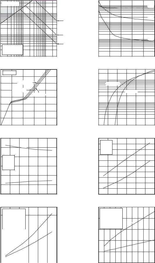
Typical Performance Curves
RC MODEL
Junction temp. ( ”C)
|
0.0271 |
0.00899F |
|
Power |
0.0656 |
0.0202F |
|
(Watts) |
|||
|
|
||
|
0.0859 |
0.293F |
Case temperature 
FIGURE2, TRANSIENT THERMAL IMPEDANCE MODEL
|
250 |
|
|
|
|
|
|
|
|
|
VDS> ID (ON) x RDS(ON) MAX. |
|
|
|
|
(AMPERES) |
|
|
250 µSEC. PULSE TEST |
|
|
|
|
200 |
|
@ <0.5 % DUTY CYCLE |
|
|
|
||
|
|
|
|
|
|
||
150 |
|
|
|
|
|
|
|
DRAIN CURRENT |
100 |
|
|
|
|
|
|
50 |
|
|
TJ = +25°C |
|
|
|
|
, |
|
|
|
|
|
|
|
D |
|
|
TJ |
= +125°C |
|
|
|
I |
|
|
|
TJ = -55°C |
|
||
|
|
|
|
|
|||
|
|
|
|
|
|
|
|
|
0 |
0 |
2 |
4 |
6 |
8 |
10 |
|
|
VGS, GATE-TO-SOURCE VOLTAGE (VOLTS) |
|||||
FIGURE4, TRANSFERCHARACTERISTICS
120
(AMPERES) |
100 |
|
|
|
|
|
|
|
|
|
|
|
|
|
|
|
|
|
|
|
|
|
|
|
|
|
|
|
|
||
80 |
|
|
|
|
|
|
|
|
|
|
|
|
|
|
|
CURRENT |
|
|
|
|
|
|
|
|
|
|
|
|
|
|
|
60 |
|
|
|
|
|
|
|
|
|
|
|
|
|
|
|
|
|
|
|
|
|
|
|
|
|
|
|
|
|
|
|
,DRAIN |
40 |
|
|
|
|
|
|
|
|
|
|
|
|
|
|
|
|
|
|
|
|
|
|
|
|
|
|
|
|
||
20 |
|
|
|
|
|
|
|
|
|
|
|
|
|
|
|
D |
|
|
|
|
|
|
|
|
|
|
|
|
|
|
|
|
|
|
|
|
|
|
|
|
|
|
|
|
|
||
I |
|
|
|
|
|
|
|
|
|
|
|
|
|
|
|
|
0 |
|
|
|
|
|
|
|
|
|
|
|
|
|
|
|
25 |
50 |
|
75 |
|
100 |
125 |
|
150 |
||||||
|
|
|
|
TC, CASE TEMPERATURE (°C) |
|
|
|||||||||
FIGURE6,MAXIMUMDRAINCURRENTvsCASETEMPERATURE |
|||||||||||||||
RESISTANCE |
2.5 |
|
|
|
|
|
|
|
|
|
|
|
|
|
|
|
|
|
ID = 50A |
|
|
|
|
|
|
|
|
|
|
||
|
|
|
VGS = 10V |
|
|
|
|
|
|
|
|
|
|
||
SOURCE-TO-DRAINON (NORMALIZED) |
2.0 |
|
|
|
|
|
|
|
|
|
|
|
|
|
|
|
|
|
|
|
|
|
|
|
|
|
|
|
|
||
1.5 |
|
|
|
|
|
|
|
|
|
|
|
|
|
|
|
|
|
|
|
|
|
|
|
|
|
|
|
|
|
||
|
|
|
|
|
|
|
|
|
|
|
|
|
|
|
|
|
1.0 |
|
|
|
|
|
|
|
|
|
|
|
|
|
|
|
|
|
|
|
|
|
|
|
|
|
|
|
|
|
|
|
|
|
|
|
|
|
|
|
|
|
|
|
|
|
|
, |
0.5 |
|
|
|
|
|
|
|
|
|
|
|
|
|
|
|
|
|
|
|
|
|
|
|
|
|
|
|
|
||
|
|
|
|
|
|
|
|
|
|
|
|
|
|
||
|
|
|
|
|
|
|
|
|
|
|
|
|
|
|
|
DS(ON) |
0.0 |
|
|
|
|
|
|
|
|
|
|
|
|
|
|
|
|
|
|
|
|
|
|
|
|
|
|
|
|
||
|
-25 0 |
25 50 |
75 |
100 125 |
150 |
||||||||||
R |
-50 |
||||||||||||||
TJ, JUNCTION TEMPERATURE (°C)
FIGURE 8, RDS(ON) vs. TEMPERATURE
|
250 |
|
|
|
|
|
|
APT30M30B2LL_LLL |
|||
|
|
|
|
|
VGS =15 &10V |
|
|
|
|||
|
|
|
|
|
|
|
|
|
|||
(AMPERES) |
|
|
|
|
|
|
8V |
|
|
|
|
200 |
|
|
|
|
|
|
|
|
|
|
|
|
|
|
|
|
|
7.5V |
|
|
|
|
|
150 |
|
|
|
|
|
|
|
|
|
|
|
CURRENT |
|
|
|
|
|
|
|
7V |
|
|
|
100 |
|
|
|
|
|
|
|
6.5 |
|
|
|
|
|
|
|
|
|
|
|
|
|
||
DRAIN |
50 |
|
|
|
|
|
|
|
|
6V |
|
, |
|
|
|
|
|
|
|
|
|
|
|
D |
|
|
|
|
|
|
|
|
|
|
|
I |
|
|
|
|
|
|
|
|
|
5.5V |
|
|
|
|
|
|
|
|
|
|
|
||
|
0 0 |
|
5 |
10 |
|
15 |
20 |
25 |
30 |
||
|
|
VDS, DRAIN-TO-SOURCE VOLTAGE (VOLTS) |
|||||||||
|
FIGURE3,LOW VOLTAGE OUTPUTCHARACTERISTICS |
||||||||||
RESISTANCE |
1.40 |
|
|
|
|
|
|
|
|
|
|
|
|
|
NORMALIZED TO |
|
|
|
|
|
|||
1.30 |
|
VGS = 10V |
@ ID = 50A |
|
|
|
|
||||
|
|
|
|
|
|
|
|
|
|
||
|
|
|
|
|
|
|
|
|
|
|
|
ON |
1.20 |
|
|
|
|
|
|
|
|
|
|
|
|
|
|
|
|
|
|
|
|
|
|
DRAIN-TO-SOURCE |
1.10 |
|
|
|
|
VGS=10V |
|
|
|
|
|
|
|
|
|
|
|
|
|
|
|||
1.00 |
|
|
|
|
|
|
|
|
|
|
|
0.90 |
|
|
|
|
|
|
VGS=20V |
|
|
||
|
|
|
|
|
|
|
|
|
|
||
, |
|
|
|
|
|
|
|
|
|
|
|
DS(ON) |
0.80 |
0 |
20 |
40 |
60 |
80 |
100 |
120 |
140 |
160 |
180 |
R |
|
||||||||||
|
|
|
|
ID, DRAIN CURRENT (AMPERES) |
|
||||||
FIGURE 5, RDS(ON) vs DRAIN CURRENT
BREAKDOWNSOURCE-TO-DRAIN |
(NORMALIZED)VOLTAGE |
1.15 |
|
|
|
|
|
|
|
|
|
|
|
|
|
|
|
|
|
0.95 |
|
|
|
|
|
|
|
|
|
|
|
|
|
|
|
|
|
||
|
|
|
|
|
|
|
|
|
|
|
|
|
|
|
|
|
|||
|
|
1.10 |
|
|
|
|
|
|
|
|
|
|
|
|
|
|
|
|
|
|
|
1.05 |
|
|
|
|
|
|
|
|
|
|
|
|
|
|
|
|
|
|
|
|
|
|
|
|
|
|
|
|
|
|
|
|
|
|
|
|
|
|
|
|
|
|
|
|
|
|
|
|
|
|
|
|
|
|
|
|
|
, |
|
1.00 |
|
|
|
|
|
|
|
|
|
|
|
|
|
|
|
|
|
|
|
|
|
|
|
|
|
|
|
|
|
|
|
|
|
|
|
||
|
|
|
|
|
|
|
|
|
|
|
|
|
|
|
|
|
|
||
|
|
|
|
|
|
|
|
|
|
|
|
|
|
|
|
|
|
|
|
|
|
|
|
|
|
|
|
|
|
|
|
|
|
|
|
|
|
|
|
|
|
|
|
|
|
|
|
|
|
|
|
|
|
|
|
|
|
|
|
DSS |
|
|
|
|
|
|
|
|
|
|
|
|
|
|
|
|
|
|
|
BV |
|
0.90- |
|
|
|
|
|
|
|
|
|
|
|
|
|
|
|
|
|
|
|
50 |
-25 |
0 |
25 |
50 |
75 |
100 125 |
150 |
||||||||||
|
|
|
|
|
TJ, JUNCTION TEMPERATURE (°C) |
|
|
||||||||||||
|
|
FIGURE7,BREAKDOWNVOLTAGEvsTEMPERATURE |
|||||||||||||||||
|
|
1.2 |
|
|
|
|
|
|
|
|
|
|
|
|
|
|
|
|
|
THRESHOLDVOLTAGE |
|
1.1 |
|
|
|
|
|
|
|
|
|
|
|
|
|
|
|
|
|
|
|
|
|
|
|
|
|
|
|
|
|
|
|
|
|
|
|
||
|
|
|
|
|
|
|
|
|
|
|
|
|
|
|
|
|
|||
(NORMALIZED) |
1.0 |
|
|
|
|
|
|
|
|
|
|
|
|
|
|
|
|
|
|
|
|
|
|
|
|
|
|
|
|
|
|
|
|
|
|
|
|||
|
|
|
|
|
|
|
|
|
|
|
|
|
|
|
|
||||
0.8 |
|
|
|
|
|
|
|
|
|
|
|
|
|
|
|
|
|
||
|
|
|
|
|
|
|
|
|
|
|
|
|
|
|
|
|
|||
, |
|
0.9 |
|
|
|
|
|
|
|
|
|
|
|
|
|
|
|
|
|
|
|
|
|
|
|
|
|
|
|
|
|
|
|
|
|
|
|||
|
|
|
|
|
|
|
|
|
|
|
|
|
|
|
|
|
|
|
|
|
|
|
|
|
|
|
|
|
|
|
|
|
|
|
|
|
|
|
|
|
|
|
|
|
|
|
|
|
|
|
|
|
|
|
|
|
|
|
|
GS(TH) |
0.7 |
|
|
|
|
|
|
|
|
|
|
|
|
|
|
|
|
|
|
|
|
|
|
|
|
|
|
|
|
|
|
|
|
|
|
|
|||
|
|
|
|
|
|
|
|
|
|
|
|
|
|
|
|
||||
V |
|
|
|
|
|
|
|
|
|
|
|
|
|
|
|
|
|
|
|
|
|
0.6- |
|
|
|
|
|
|
|
|
|
|
|
|
|
|
|
|
|
|
|
|
|
|
|
|
|
|
|
|
|
|
|
|
|
|
|
|
|
|
|
50 |
-25 |
0 |
25 |
50 |
75 |
100 125 |
150 |
||||||||||
|
|
|
|
|
|
TC, CASE TEMPERATURE (°C) |
|
|
|||||||||||
FIGURE9,THRESHOLDVOLTAGEvsTEMPERATURE
050-7153 Rev B 7-2004
|
400 |
OPERATIONHERE |
|
|
||
|
|
|
|
|||
|
|
LIMITEDBYRDS(ON) |
|
|
||
CURRENT (AMPERES) |
100 |
|
|
|
|
|
|
|
|
|
|
100µS |
|
10 |
|
|
|
|
1mS |
|
DRAIN |
|
T |
|
=+25°C |
|
10mS |
, |
|
|
|
|
||
D |
|
|
|
|
||
I |
|
C |
|
|
|
|
|
|
TJ |
=+150°C |
|
|
|
|
1 |
SINGLE PULSE |
|
|
||
|
1 |
|
10 |
100 |
300 |
|
|
|
VDS, DRAIN-TO-SOURCE VOLTAGE (VOLTS) |
||||
|
|
FIGURE10,MAXIMUMSAFEOPERATINGAREA |
||||
(VOLTS) |
16 |
ID = 100A |
|
|
|
|
|
|
|
|
|
||
|
|
VDS=60V |
|
|
|
|
VOLTAGE |
12 |
|
|
|
|
|
|
VDS=150V |
|
|
|
||
|
|
|
VDS=240V |
|
||
GATE-TO-SOURCE |
8 |
|
|
|
||
|
|
|
|
|
||
4 |
|
|
|
|
|
|
|
|
|
|
|
|
|
, |
|
|
|
|
|
|
GS |
|
|
|
|
|
|
V |
0 0 |
|
|
|
|
|
|
50 |
100 |
150 |
200 |
250 |
|
|
|
Qg, TOTAL GATE CHARGE (nC) |
|
|||
FIGURE12,GATECHARGEvsGATE-TO-SOURCEVOLTAGE
|
120 |
|
|
|
|
|
|
|
|
|
100 |
|
|
|
|
td(off) |
|
|
|
|
|
|
|
|
|
|
|
|
|
(ns) |
80 |
VDD = 300V |
|
|
|
|
|
||
|
RG = 5Ω |
|
|
|
|
|
|||
d(off) |
|
|
|
|
|
|
|||
60 |
T |
J |
= 125°C |
|
|
|
|
|
|
t |
|
|
|
|
|
|
|
||
and |
L = 100µH |
|
|
|
|
|
|||
|
|
|
|
|
|
||||
|
|
|
|
|
|
|
|
|
|
d(on) |
40 |
|
|
|
|
td(on) |
|
|
|
|
|
|
|
|
|
|
|||
t |
|
|
|
|
|
|
|
||
|
|
|
|
|
|
|
|
||
|
20 |
|
|
|
|
|
|
|
|
|
0 |
|
|
|
|
|
|
|
|
|
40 |
|
|
60 |
80 |
100 |
120 |
140 |
160 |
|
|
|
|
|
|
ID (A) |
|
|
|
|
FIGURE 14, DELAY TIMES vs CURRENT |
||||||||
|
3500 |
|
|
|
|
|
|
|
|
|
|
VDD = 200V |
|
|
|
|
|
||
|
3000 |
RG = 5Ω |
|
|
|
|
|
||
|
|
TJ = 125°C |
|
|
|
|
|
||
|
J)( |
2500 |
|
|
L = 100µH |
|
|
|
|
|
|
|
|
|
||
|
|
|
|
|
|
|
|
|
|
|
|
|
|
|||
|
ENERGY |
|
|
|
EON |
includes |
|
|
|
|
|
|
|
|
|
|
|
|
|
|
|
|
|
|
|
|
|
|
|
||||
|
|
|
|
diode reverse recovery. |
|
|
|
|
||||||||
|
|
2000 |
|
|
|
|
|
|
|
|
|
|
|
|
|
|
|
|
|
|
|
|
|
|
|
|
|
|
|
|
|
|
|
|
SWITCHING |
|
|
|
|
|
|
|
Eoff |
|
|
|
|
|||
2004- |
1500 |
|
|
|
|
|
|
|
|
|
|
|
||||
|
|
|
|
|
|
|
Eon |
|
|
|
|
|||||
|
|
|
|
|
|
|
|
|
|
|
|
|
|
|
|
|
7 |
|
1000 |
|
|
|
|
|
|
|
|
|
|
|
|
|
|
|
|
|
|
|
|
|
|
|
|
|
|
|
|
|
||
|
500 |
|
|
|
|
|
|
|
|
|
|
|
|
|
|
|
B |
|
|
|
|
|
|
|
|
|
|
|
|
|
|
|
|
|
|
|
|
|
|
|
|
|
|
|
|
|
|
|
||
|
|
|
|
|
|
|
|
|
|
|
|
|
|
|
|
|
Rev |
|
0 |
|
|
|
|
|
|
|
|
|
|
|
|
|
|
|
40 |
|
60 |
80 |
100 |
120 |
140 |
160 |
||||||||
7153-050 |
|
|
|
|
|
|
|
|
|
ID (A) |
|
|
|
|
||
|
FIGURE 16, SWITCHING ENERGY vs CURRENT |
|||||||||||||||
|
|
|||||||||||||||
|
20,000 |
|
|
|
|
APT30M30B2LL_LLL |
|
|
|
|
|
|
|
|
|
|
10,000 |
|
|
|
|
|
Ciss |
(pF) |
|
|
|
|
|
|
Coss |
CAPACITANCE |
1,000 |
|
|
|
|
|
|
|
|
|
|
|
|
|
|
C, |
100 |
|
|
|
|
|
Crss |
|
10 |
0 |
10 |
20 |
30 |
40 |
50 |
|
|
VDS, DRAIN-TO-SOURCE VOLTAGE (VOLTS) |
|||||
|
FIGURE11, CAPACITANCEvsDRAIN-TO-SOURCEVOLTAGE |
||||||
(AMPERES) |
300 |
|
|
|
|
|
|
100 |
|
TJ =+150°C |
|
|
|
||
CURRENT |
|
|
|
|
TJ =+25°C |
|
|
DRAINREVERSE, |
|
|
|
|
|
|
|
10 |
|
|
|
|
|
|
|
|
|
|
|
|
|
|
|
DR |
10.3 |
|
0.5 |
0.7 |
0.9 |
1.1 |
1.3 |
1.5 |
|
I |
|
||||||||
|
|
VSD, SOURCE-TO-DRAIN VOLTAGE (VOLTS) |
|||||||
|
FIGURE13, SOURCE-DRAINDIODEFORWARDVOLTAGE |
||||||||
|
200 |
|
|
|
|
|
|
|
|
|
180 |
VDD = 200V |
|
|
|
|
|
||
|
RG |
= 5Ω |
|
|
|
|
|
||
|
|
|
|
|
|
|
|||
|
160 |
TJ = 125°C |
|
|
|
|
|
||
|
140 |
L = 100µH |
|
|
|
|
|
||
|
|
|
|
|
|
|
|
|
|
(ns) |
120 |
|
|
|
|
tf |
|
|
|
|
|
|
|
|
|
|
|
||
|
|
|
|
|
|
|
|
|
|
f |
100 |
|
|
|
|
|
|
|
|
t |
|
|
|
|
|
|
|
|
|
and |
80 |
|
|
|
|
|
|
|
|
t |
|
|
|
|
|
|
|
|
|
r |
|
|
|
|
|
|
|
|
|
|
60 |
|
|
|
|
|
tr |
|
|
|
|
|
|
|
|
|
|
|
|
|
40 |
|
|
|
|
|
|
|
|
|
20 |
|
|
|
|
|
|
|
|
|
0 |
|
|
|
|
|
|
|
|
|
40 |
|
60 |
80 |
100 |
120 |
140 |
160 |
|
|
|
|
|
|
|
ID (A) |
|
|
|
|
FIGURE 15, RISE AND FALL TIMES vs CURRENT |
||||||||
|
5000 |
VDD = 200V |
|
|
|
|
|
||
|
|
|
|
|
|
|
|||
|
|
ID = 100A |
|
|
|
|
|
||
( J) |
4000 |
TJ = 125°C |
|
|
|
|
|
||
|
L = 100µH |
|
Eoff |
|
|
|
|||
|
E |
ON |
includes |
|
|
|
|
||
ENERGY |
|
|
|
|
|
|
|
|
|
300 |
diode reverse recovery. |
|
|
|
|
||||
|
|
|
|
|
|||||
SWITCHING |
|
|
|
|
|
|
|
|
|
2000 |
|
|
|
|
|
|
|
|
|
|
|
|
|
|
|
|
|
|
|
|
|
|
|
|
|
|
|
Eon |
|
|
1000 |
|
|
|
|
|
|
|
|
|
0 |
|
|
|
|
|
|
|
|
0 5 10 15 20 25 30 35 40 45 50 RG, GATE RESISTANCE (Ohms)
FIGURE 17, SWITCHING ENERGY VS. GATE RESISTANCE

Typical Performance Curves
10% |
GateVoltage |
TJ125°C
td(on)
|
|
|
|
|
|
tr |
|
Drain Current |
|
|
|
|||
|
90% |
|
||
|
|
|
||
|
|
|
|
|
5% |
10% |
5% |
||
|
Drain Voltage |
|||
|
|
|
|
|
Switching Energy
Figure18,Turn-onSwitchingWaveformsandDefinitions
APT60DS30
VDD |
ID |
VDS |
 G
G
D.U.T.
Figure 20, Inductive Switching Test Circuit
APT30M30B2LL_LLL
90%
GateVoltage
TJ125°C
td(off)
|
Drain Voltage |
|
tf |
|
90% |
|
10% 0 |
Switching Energy |
Drain Current |
|
Figure 19, Turn-off Switching Waveforms and Definitions
T-MAXTM (B2) Package Outline |
TO-264 (L) Package Outline |
4.69 (.185) |
|
|
4.60 |
(.181) |
|
|
5.31 (.209) |
|
15.49 (.610) |
5.21 |
(.205) |
19.51 (.768) |
|
1.49 (.059) |
|
16.26 (.640) |
1.80 |
(.071) |
20.50 (.807) |
|
2.49 (.098) |
|
|
2.01 |
(.079) |
|
3.10 (.122) |
|
|
|
|
|
|
|
|
|
5.38 (.212) |
|
|
|
3.48 (.137) |
|
|
6.20 (.244) |
|
|
|
|
|
|
|
|
|
5.79 (.228) |
|
Drain |
20.80 (.819) |
|
|
|
6.20 (.244) |
|
21.46 (.845) |
Drain |
|
|
|
|
|
|
|
26.49 (1.043) |
|
|||
|
|
|
|
25.48 (1.003) |
|
|
|
4.50 (.177) Max. |
2.87 (.113) |
|
|
|
|
|
3.12 (.123) |
|
|
|
2.29 (.090) |
|
|
|
|
|
|
||
|
|
1.65 (.065) |
|
|
2.29 (.090) |
2.69 (.106) |
0.40 (.016) |
|
|
|
2.69 (.106) |
|
|
0.79 (.031) |
19.81 (.780) |
2.13 (.084) |
|
19.81 (.780) |
Gate |
|
|
20.32 (.800) |
Gate |
|
|||
|
|
21.39 (.842) |
||||
|
1.01 (.040) |
Drain |
|
|
|
Drain |
|
1.40 (.055) |
|
|
|
||
|
|
Source |
|
|
|
Source |
|
|
|
0.48 |
(.019) |
0.76 (.030) |
|
2.21 (.087) |
|
|
0.84 |
(.033) |
1.30 (.051) |
|
|
|
2.59 |
(.102) |
2.79 (.110) |
|
|
2.59 (.102) |
5.45 (.215) BSC |
3.00 |
(.118) |
3.18 (.125) |
|
|
2-Plcs. |
|
|
5.45 (.215) BSC |
||
These dimensions are equal to the TO-247 without the mounting hole. |
||
2-Plcs. |
||
|
Dimensions in Millimeters and (Inches) Dimensions in Millimeters and (Inches)
APT’s products are covered by one or more of U.S.patents 4,895,810 5,045,903 5,089,434 5,182,234 5,019,522
5,262,336 6,503,786 5,256,583 4,748,103 5,283,202 5,231,474 5,434,095 5,528,058 and foreign patents. US and Foreign patents pending. All Rights Reserved.
050-7153 Rev B 7-2004