

Features
•Low-voltage and Standard-voltage Operation
–2.7 (VCC = 2.7V to 5.5V)
–1.8 (VCC = 1.8V to 5.5V)
•Internally Organized 128 x 8 (1K), 256 x 8 (2K), 512 x 8 (4K), 1024 x 8 (8K) or 2048 x 8 (16K)
•Two-wire Serial Interface
•Schmitt Trigger, Filtered Inputs for Noise Suppression
•Bidirectional Data Transfer Protocol
•100 kHz (1.8V) and 400 kHz (2.7V, 5V) Compatibility
•Write Protect Pin for Hardware Data Protection
•8-byte Page (1K, 2K), 16-byte Page (4K, 8K, 16K) Write Modes
•Partial Page Writes Allowed
•Self-timed Write Cycle (5 ms max)
•High-reliability
–Endurance: 1 Million Write Cycles
–Data Retention: 100 Years
•Automotive Grade and Lead-free/Halogen-free Devices Available
•8-lead PDIP, 8-lead JEDEC SOIC, 8-lead MAP, 5-lead SOT23, 8-lead TSSOP and 8-ball dBGA2 Packages
•Die Sales: Wafer Form, Waffle Pack and Bumped Wafers
Description
The AT24C01A/02/04/08A/16A provides 1024/2048/4096/8192/16384 bits of serial electrically erasable and programmable read-only memory (EEPROM) organized as 128/256/512/1024/2048 words of 8 bits each. The device is optimized for use in many industrial and commercial applications where low-power and low-voltage operation are essential. The AT24C01A/02/04/08A/16A is available in space-saving 8-lead PDIP, 8-lead JEDEC SOIC, 8-lead MAP, 5-lead SOT23 (AT24C01A/AT24C02/AT24C04), 8- lead TSSOP, and 8-ball dBGA2 packages and is accessed via a Two-wire serial interface. In addition, the entire family is available in 2.7V (2.7V to 5.5V) and 1.8V (1.8V to 5.5V) versions.
8-lead TSSOP
Table 1. Pin Configuration |
|
|
|
|
|
|
|
|
|
|
|
A0 |
|
1 |
|
8 |
|
|
VCC |
||||
Pin Name |
Function |
|
|
|
|
||||||
|
|
|
|
||||||||
|
|
|
|
||||||||
|
|
A1 |
|
2 |
|
7 |
|
|
WP |
||
A0 - A2 |
Address Inputs |
A2 |
|
3 |
|
6 |
|
|
SCL |
||
|
|
|
|
||||||||
|
|
|
|
|
|
||||||
|
|
GND |
|
4 |
|
5 |
|
|
SDA |
||
SDA |
Serial Data |
|
|
|
|
||||||
|
|
|
|
||||||||
|
|
|
|
||||||||
|
|
|
|
|
|
|
|
|
|
|
|
SCL |
Serial Clock Input |
|
|
|
|
|
|
|
|
|
|
|
|
8-ball dBGA2 |
|
||||||||
|
|
|
|
|
|||||||
WP |
Write Protect |
|
|
|
|||||||
|
|
|
|
|
|
|
|
|
|
||
|
|
VCC |
8 |
1 |
|
A0 |
|
||||
NC |
No Connect |
|
|
||||||||
WP |
7 |
2 |
|
A1 |
|
||||||
|
|
|
|
||||||||
GND |
Ground |
|
|||||||||
SCL |
6 |
3 |
|
A2 |
|
||||||
|
|
SDA |
5 |
4 |
|
GND |
|||||
VCC |
Power Supply |
|
|||||||||
|
|
|
|
|
|
|
|
|
|
||
|
|
|
|
Bottom View |
|
||||||
|
|
|
|
|
|||||||
|
|
|
8-lead PDIP |
|
|||||||
|
|
|
|
|
|
|
|
|
|
|
|
|
|
A0 |
|
1 |
|
8 |
|
VCC |
|||
|
|
|
|
|
|||||||
|
|
A1 |
|
2 |
|
7 |
|
WP |
|
||
|
|
|
|
|
|
||||||
|
|
A2 |
|
3 |
|
6 |
|
SCL |
|||
|
|
|
|
|
|||||||
|
|
GND |
|
4 |
|
5 |
|
SDA |
|||
|
|
|
|
|
|||||||
|
|
|
|
|
|
|
|
|
|
|
|
8-lead SOIC
A0 |
|
1 |
8 |
|
VCC |
|
|
||||
A1 |
|
2 |
7 |
|
WP |
|
|
||||
A2 |
|
3 |
6 |
|
SCL |
|
|
||||
GND |
|
4 |
5 |
|
SDA |
|
|
||||
|
|
|
|
|
|
8-lead MAP
VCC |
|
|
|
|
A0 |
||
8 |
|
1 |
|||||
WP |
|
|
|
|
A1 |
||
7 |
2 |
||||||
SCL |
|
|
|
|
A2 |
||
6 |
3 |
||||||
SDA |
|
|
|
|
GND |
||
5 |
4 |
||||||
|
|
|
|
|
|
||
|
|
Bottom View |
|
|
|||
|
|
5-lead SOT23 |
|||||
|
|
|
|
|
|
WP |
|
SCL |
|
|
1 |
5 |
|
||
|
|
|
|||||
GND |
|
|
2 |
|
|
|
VCC |
|
|
|
|
|
|||
SDA |
|
|
3 |
4 |
|
||
|
|
|
|||||
|
|
|
|
|
|
|
|
Two-wire
Serial EEPROM
1K (128 x 8)
2K (256 x 8)
4K (512 x 8)
8K (1024 x 8)
16K (2048 x 8)
AT24C01A
AT24C02
AT24C04
AT24C08A
AT24C16A
0180V–SEEPR–8/05
1
Absolute Maximum Ratings
..................................Operating Temperature |
–55°C to +125°C |
*NOTICE: Stresses beyond those listed under “Absolute |
|
|
Maximum Ratings” may cause permanent dam- |
Storage Temperature ..................................... |
–65°C to +150°C |
age to the device. This is a stress rating only and |
|
|
functional operation of the device at these or any |
Voltage on Any Pin |
|
other conditions beyond those indicated in the |
with Respect to Ground .................................... |
–1.0V to +7.0V |
operational sections of this specification is not |
Maximum Operating Voltage |
6.25V |
implied. Exposure to absolute maximum rating |
conditions for extended periods may affect device |
||
DC Output Current |
5.0 mA |
reliability. |
|
||
|
|
|
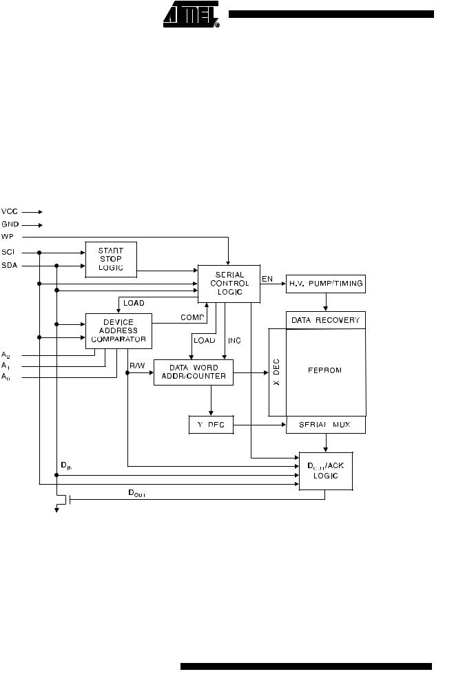
Figure 1. Block Diagram
2 AT24C01A/02/04/08A/16A
0180V–SEEPR–8/05

 AT24C01A/02/04/08A/16A
Pin Description
SERIAL CLOCK (SCL): The SCL input is used to positive edge clock data into each EEPROM device and negative edge clock data out of each device.
SERIAL DATA (SDA): The SDA pin is bidirectional for serial data transfer. This pin is open-drain driven and may be wire-ORed with any number of other open-drain or opencollector devices.
DEVICE/PAGE ADDRESSES (A2, A1, A0): The A2, A1 and A0 pins are device address inputs that are hard wired for the AT24C01A and the AT24C02. As many as eight 1K/2K devices may be addressed on a single bus system (device addressing is discussed in detail under the Device Addressing section).
The AT24C04 uses the A2 and A1 inputs for hard wire addressing and a total of four 4K devices may be addressed on a single bus system. The A0 pin is a no connect.
The AT24C08A only uses the A2 input for hardwire addressing and a total of two 8K devices may be addressed on a single bus system. The A0 and A1 pins are no connects.
The AT24C16A does not use the device address pins, which limits the number of devices on a single bus to one. The A0, A1 and A2 pins are no connects.
WRITE PROTECT (WP): The AT24C01A/02/04/08A/16A has a Write Protect pin that provides hardware data protection. The Write Protect pin allows normal Read/Write operations when connected to ground (GND). When the Write Protect pin is connected to VCC, the write protection feature is enabled and operates as shown in Table 2.
Table 2. |
Write Protect |
|
|
|
|
|
|
|
|
|
|
|
|
|
|
WP Pin |
|
|
|
Part of the Array Protected |
|
||
|
|
|
|
|
|
|
|
Status |
|
24C01A |
24C02 |
|
24C04 |
24C08A |
24C16A |
|
|
|
|
|
|
|
|
At VCC |
|
Full (1K) |
Full (2K) |
|
Full (4K) |
Full (8K) |
Full (16K) |
|
Array |
Array |
|
Array |
Array |
Array |
|
|
|
|
|||||
|
|
|
|
|
|
|
|
At GND |
|
Normal Read/Write Operations |
|
|
|||
|
|
|
|
|
|
|
|
Memory Organization AT24C01A, 1K SERIAL EEPROM: Internally organized with 16 pages of 8 bytes each, the 1K requires a 7-bit data word address for random word addressing.
AT24C02, 2K SERIAL EEPROM: Internally organized with 32 pages of 8 bytes each, the 2K requires an 8-bit data word address for random word addressing.
AT24C04, 4K SERIAL EEPROM: Internally organized with 32 pages of 16 bytes each, the 4K requires a 9-bit data word address for random word addressing.
AT24C08A, 8K SERIAL EEPROM: Internally organized with 64 pages of 16 bytes each, the 8K requires a 10-bit data word address for random word addressing.
AT24C16A, 16K SERIAL EEPROM: Internally organized with 128 pages of 16 bytes each, the 16K requires an 11-bit data word address for random word addressing.
3
0180V–SEEPR–8/05

Table 3. Pin Capacitance(1)
Applicable over recommended operating range from TA = 25°C, f = 1.0 MHz, VCC = +1.8V
Symbol |
|
Test Condition |
Max |
Units |
Conditions |
|
|
|
|
|
|
CI/O |
|
Input/Output Capacitance (SDA) |
8 |
pF |
VI/O = 0V |
CIN |
|
Input Capacitance (A0, A1, A2, SCL) |
6 |
pF |
VIN = 0V |
Note: 1. |
This parameter is characterized and is not 100% tested. |
|
|
|
|
Table 4. DC Characteristics
Applicable over recommended operating range from: TAI = –40°C to +85°C, VCC = +1.8V to +5.5V, VCC = +1.8V to +5.5V (unless otherwise noted)
Symbol |
|
Parameter |
Test Condition |
Min |
Typ |
Max |
Units |
|
|
|
|
|
|
|
|
VCC1 |
|
Supply Voltage |
|
1.8 |
|
5.5 |
V |
VCC2 |
|
Supply Voltage |
|
2.7 |
|
5.5 |
V |
VCC3 |
|
Supply Voltage |
|
4.5 |
|
5.5 |
V |
ICC |
|
Supply Current VCC = 5.0V |
READ at 100 kHz |
|
0.4 |
1.0 |
mA |
ICC |
|
Supply Current VCC = 5.0V |
WRITE at 100 kHz |
|
2.0 |
3.0 |
mA |
ISB1 |
|
Standby Current VCC = 1.8V |
VIN = VCC or VSS |
|
0.6 |
3.0 |
µA |
ISB2 |
|
Standby Current VCC = 2.5V |
VIN = VCC or VSS |
|
1.4 |
4.0 |
µA |
ISB3 |
|
Standby Current VCC = 2.7V |
VIN = VCC or VSS |
|
1.6 |
4.0 |
µA |
ISB4 |
|
Standby Current VCC = 5.0V |
VIN = VCC or VSS |
|
8.0 |
18.0 |
µA |
ILI |
|
Input Leakage Current |
VIN = VCC or VSS |
|
0.10 |
3.0 |
µA |
ILO |
|
Output Leakage Current |
VOUT = VCC or VSS |
|
0.05 |
3.0 |
µA |
VIL |
|
Input Low Level(1) |
|
–0.6 |
|
VCC x 0.3 |
V |
VIH |
|
Input High Level(1) |
|
VCC x 0.7 |
|
VCC + 0.5 |
V |
VOL2 |
|
Output Low Level VCC = 3.0V |
IOL = 2.1 mA |
|
|
0.4 |
V |
VOL1 |
|
Output Low Level VCC = 1.8V |
IOL = 0.15 mA |
|
|
0.2 |
V |
Note: 1. |
VIL min and VIH max are reference only and are not tested. |
|
|
|
|
||
4 AT24C01A/02/04/08A/16A
0180V–SEEPR–8/05

 AT24C01A/02/04/08A/16A
Table 5. AC Characteristics
Applicable over recommended operating range from TAI = –40°C to +85°C, VCC = +1.8V to +5.5V, VCC = +2.7V to +5.5V, CL = 1 TTL Gate and 100 pF (unless otherwise noted)
|
|
1.8-volt |
2.7, 5.0-volt |
|
||
|
|
|
|
|
|
|
Symbol |
Parameter |
Min |
Max |
Min |
Max |
Units |
|
|
|
|
|
|
|
fSCL |
Clock Frequency, SCL |
|
100 |
|
400 |
kHz |
tLOW |
Clock Pulse Width Low |
4.7 |
|
1.2 |
|
µs |
tHIGH |
Clock Pulse Width High |
4.0 |
|
0.6 |
|
µs |
tI |
Noise Suppression Time(1) |
|
100 |
|
50 |
ns |
tAA |
Clock Low to Data Out Valid |
0.1 |
4.5 |
0.1 |
0.9 |
µs |
tBUF |
Time the bus must be free before |
4.7 |
|
1.2 |
|
µs |
a new transmission can start(1) |
|
|
||||
tHD.STA |
Start Hold Time |
4.0 |
|
0.6 |
|
µs |
tSU.STA |
Start Setup Time |
4.7 |
|
0.6 |
|
µs |
tHD.DAT |
Data In Hold Time |
0 |
|
0 |
|
µs |
tSU.DAT |
Data In Setup Time |
200 |
|
100 |
|
ns |
tR |
Inputs Rise Time(1) |
|
1.0 |
|
0.3 |
µs |
tF |
Inputs Fall Time(1) |
|
300 |
|
300 |
ns |
tSU.STO |
Stop Setup Time |
4.7 |
|
0.6 |
|
µs |
tDH |
Data Out Hold Time |
100 |
|
50 |
|
ns |
tWR |
Write Cycle Time |
|
5 |
|
5 |
ms |
Endurance(1) |
5.0V, 25°C, Byte Mode |
1M |
|
1M |
|
Write |
|
|
Cycles |
||||
|
|
|
|
|
|
|
|
|
|
|
|
|
|
Note: 1. This parameter is characterized.
5
0180V–SEEPR–8/05