

dsd11-12 / dsd-12=Проектирование РЧ КМОП ИС / papers / 96_Voltage-Comparator-Based_Measurement
.PDF726 |
IEEE JOURNAL ON SOLID-STATE CIRCUITS, VOL. 31, NO. 5, MAY 1996 |
Voltage-Comparator-Based Measurement of Equivalently Sampled Substrate Noise Waveforms in Mixed-Signal Integrated Circuits
Keiko Makie-Fukuda, Takanobu Anbo, Toshiro Tsukada, Tatsuji Matsuura, and Masao Hotta
AbstractÐThis paper describes measurement of substrate noise waveforms in mixed-signal integrated circuits. This method uses wide-band chopper-type single-ended voltage comparators as on-chip noise detectors. By analyzing equivalently sampled comparator outputs in synchronized operation, the noise voltage in the auto-zero and compare modes can be measured separately, and noise waveforms were experimentally reconstructed to within 0.5-ns accuracy. The noise transmission path was analyzed, and this showed that the noise sampled at the auto-zero mode of the comparator can be used to reconstruct substrate noise waveforms with high resolution. The results also explain the influence of noise coupling on analog circuits widely used in on-chip analog- to-digital converters.
I. INTRODUCTION
RECENTLY the demands on compact analog and digital mixed-signal integrated circuits (IC's), in which highspeed analog and large-scale digital circuits are implemented, are increasing due to multimedia applications. In these mixedsignal IC's, the noise created by the digital circuits passes to the on-chip analog circuits through the substrate and affects analog circuit performance. Therefore, it is important to be able to measure the substrate noise and estimate the coupling
of digital noise to analog circuits.
Switching noise in mixed-signal IC's has been measured with a single transistor amplifier [1]±[3]. Su et al. [3] experimentally described several approaches to reducing substrate crosstalk and discussed the effect of substrate noise reduction on the basis of their measured results. However, the measured noise value included the influence of the external parasitic impedance of the transistor amplifier in the experimental set up. To eliminate this parasitic effect and to estimate the actual influence of digital noise on on-chip analog circuits, we proposed a voltage-comparator-based noise measuring method [4], [5]. The rms voltage and the amplitude of substrate noise were measured as equivalent input voltages of actual comparators by analyzing the distribution of metastability in the on-chip comparator. From the experimental results, it was shown that the influence of digital noise can be reduced considerably by using a differential configuration of analog circuits and by lowering the digital supply voltage. However, the waveforms of substrate noise were not measured in that study.
In this paper, we propose a way to reconstruct substrate noise waveforms using the voltage-comparator-based mea-
Manuscript received May 4, 1995; revised October 12, 1995.
K. Makie-Fukuda, T. Tsukada, T. Matsuura, and M. Hotta are with the Semiconductor Development Center, Semiconductor and Integrated Circuits Division, Hitachi, Ltd., Tokyo, Japan.
T. Anbo is with Hitachi ULSI Engineering Corporation, Tokyo, Japan. Publisher Item Identifier S 0018-9200(96)03400-2.
suring method. The method, the 0.8-
 CMOS test chip configurations and the measurement system are described in Sections II, III, and IV. The experimental results and the circuit simulation for analysis of noise transmission path are described in Sections V and VI.
II. NOISE WAVEFORM RECONSTRUCTION
An on-chip voltage comparator is used to detect and reconstruct the substrate noise waveform [5]. In the comparator, input voltages 


 and
and 
 are compared, and the corresponding logic level (high or low) is output. To measure substrate noise influence with this method,


 changes with the change in input voltage
 while
while 
 is kept constant.


 is expressed by
(1)
If substrate noise is added to the input, the metastable zone, in which high and low output levels exist, becomes wider or is shifted. Then, the average voltage  and the standard deviation
  which represents the rms value of noise, can be obtained as follows:
|
(2) |
||||
|
|
|
|
|
|
|
(3) |
||||
where |
|
|
|
||
is a probability function defined as |
|||||


 is a measured probability of high output at


 Thus, substrate noise influence is observed as the equivalent input noise.
An example of a noise waveform is illustrated in Fig. 1. Noise is generally believed to be produced by the fast switching current noise, and the noise pulse generated at the rising and falling edge of the digital clock is transmitted through the substrate to the comparator. For reconstructing noise waveform, we use the comparator which is synchronized with digital circuits activated with one clock signal. The black circles represent the sampling points. The same point
is repeatedly selected to measure the sampled value. The
mean voltage |
of the distribution |
gives the sampled |
noise voltage, |
and the rms value |
represents the error |
of the measurement. The substrate noise waveform can be reconstructed from each sample value measured by slightly shifting the comparator sampling timing by 


0018±9200/96$05.00 ã 1996 IEEE

IEEE JOURNAL ON SOLID-STATE CIRCUITS, VOL. 31, NO. 5, MAY 1996 |
727 |
Fig. 1. Noise waveform reconstruction method.
(a)
(b)
Fig. 2. Voltage comparator. (a) Circuit configuration and (b) timing chart.
III.TEST CHIP FOR MEASUREMENT
A.Voltage Comparator
A chopper-type single-ended voltage comparator is used as a noise detector. Since the compared voltage level is automatically set to the most sensitive point, substrate noise can be detected with high resolution. The comparator outputs are digital, so the influence of external noise is eliminated as much as possible. The intrinsic substrate noise waveform can thus be easily reconstructed from the comparator outputs. The circuit configuration of the voltage comparator and its timing chart are shown in Fig. 2. Here, 
 is input in the auto-zero mode and
 is input in the compare mode. The differential value between
 and
and 
 is amplified by three inverters, and the result is held in the latch. The circuit ground and bulk
ground are separated on the chip so that we can detect the substrate noise accurately from the bulk node.
The noise is assumed to be detected at 
 in the auto-zero mode and at
 in the compare mode.
 is just before the transition from the auto-zero to the compare mode. The noise detected at
 becomes the offset error of the initial voltage


 is just before the transition from the compare to the auto-zero mode. The noise in the compare mode is amplified by the inverters and held in the latch at

 This noise represents the change in the compared voltage

 Output voltage


 of the first-stage inverter (gain
 can thus be
expressed as
|
|
|
(4) |
where |
is the noise at |
and |
is the noise at |
|
gives a negative change and |
gives a positive |
|
change in the comparator output. Equation (4) shows that the noise in the auto-zero mode and that in the compare mode have a different influence on comparator outputs.
The designed comparator characteristics were simulated by a circuit simulation tool. The gain and the bandwidth of the first-stage inverter are 24 dB and 300 MHz, respectively. The input bandwidths are 3 GHz in the auto-zero mode and 300 MHz in the compare mode. In the compare mode, the bandwidth of the detected noise is also limited by the bandwidth of the inverter amplifiers. Since the noise detected in the auto-zero mode is kept as a dc offset value, this bandwidth is not limited by the inverter amplifier and is only influenced by the input bandwidth. The substrate noise waveform can then be detected more precisely in the auto-zero mode than in the compare mode of this comparator.
B. Test Chip Configuration
A photograph of a test chip is shown in Fig. 3. It was fabricated by 0.8-
 CMOS bulk process. The power supply voltages are supplied separately to the digital and analog circuits with separate package pins to minimize the coupling of

728 |
IEEE JOURNAL ON SOLID-STATE CIRCUITS, VOL. 31, NO. 5, MAY 1996 |
Fig. 3. Photograph of the test chip.
switching noise through the power supply lines. The substrate of the test chip (400-
 thickness) was a lightly doped p- type bulk, whose bottom is directly connected to the package frame with electric conductivity. The substrate is biased to the ground level at the surface of the chip through the heavily doped p-type diffusion. For the analog voltage comparators, circuit ground and substrate bias lines are separately connected to their own package pins to detect the noise through the substrate. The digital noise source comprises 15 k-gates CMOS inverters, consists of 24 blocks, and is controlled by a single digital clock. Each block includes four noise source groups as shown in Fig. 4(a). The simulated noise source current is shown in Fig. 4(b). The simulated noise current, which flows in both the nMOS and pMOS transistors (on) during an output transition, is directly transmitted to the substrate, since the circuit ground and the substrate of digital noise source are connected inside the cells. This noise current causes a positive voltage change at the substrate of analog circuit for digital noise measurement.
Fig. 4. Noise source CMOS inverters. (a) Implementation and (b) simulated noise current produced by noise source.
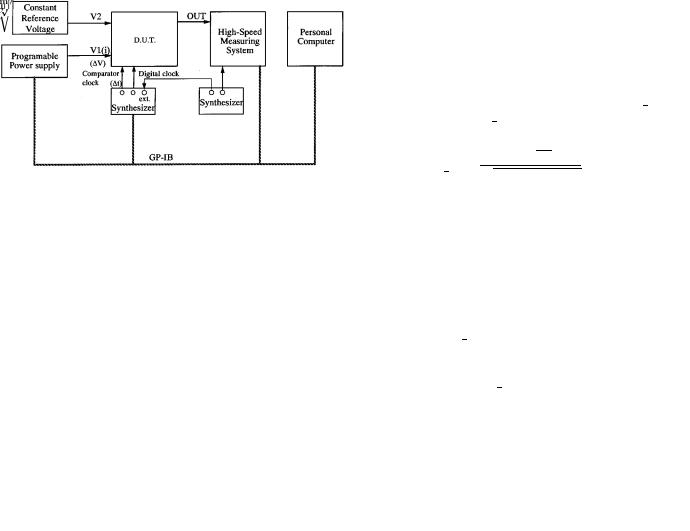
IV. MEASURING SYSTEM
The measurement conditions are shown in Table I. We chose the digital clock frequency for the noise source, which generates sharp pulse noises at the clock transitions, based on the voltage comparator clock frequency. Though the substrate noise can be measured with a resolution of 0.1 mV, 
 is determined as 0.5 mV by the limitation of the measurement equipment. The voltage comparator clock is synchronized with the digital clock. To detect the noise influence at
 and
and 
 separately, the pulse width of the digital clock is set at onefourth of the pulse period. A block diagram of the measuring system is shown in Fig. 5. A personal computer manages the overall system through a GP-IB interface bus.


 is supplied by a programmable power supply. The measured data in the high-speed measuring system [6] are sent to the personal computer, where the average and the rms value of noise at each sampling point are calculated.
The metastable zone at each sampling point is shifted by the influence of the substrate noise. To reduce the measuring time, the boundary of the metastable zone at each sampling point is found automatically. The flow is shown in Fig. 6.
TABLE I
TYPICAL MEASUREMENT CONDITIONS
First, voltage 
 is set to
 and the input voltage increment is set as


 Then the output levels are roughly measured. If there is no change in output levels,
 is shifted by


 When mixed ªhighº and ªlowº levels are measured,
 is reduced by


 as shown in Fig. 6, for example. The sequence is repeated until the increment of input voltage becomes


 The final voltage of
 is determined as minimum voltage

 After this, the distribution is measured
IEEE JOURNAL ON SOLID-STATE CIRCUITS, VOL. 31, NO. 5, MAY 1996 |
729 |
The results are shown in Fig. 8. These noise influences are due |
||
to both the body effect and capacitive coupling. Though the |
||
effect of capacitive coupling is increased with frequency, we |
||
note and discuss the body effect. |
|
|
Concerning with the body effect, the detected noise influ- |
||
ence depends on the transconductance |
|
|
The transconductance in |
the saturation region, |
and |
in the ohmic region, |
can be expressed as follows: |
|
|
|
(5) |
Fig. 5. Block diagram of the measuring system.
with the increment of input voltage 
 The maximum voltage
  is at a point five times
 higher than the voltage at
which ªhighº and ªlowº levels cease to be mixed.
V. EXPERIMENTAL RESULTS
The noise influence measured at 
 and
and 
 are collected separately for waveform reconstruction as shown in Fig. 7. Since
  was smaller than the 0.5-mV change in the input voltage, the error was small enough to reconstruct the noise waveform. The noise is referenced from the level at which the voltage settles to after the noise pulse and plotted without using any interpolation ways. The amplitude of the noise depends on the number of the activated logic gates (7.4 k-gates/3.9 k-gates). This dependence is expected from the previous measurement using voltage comparator [4], [5]. The noise changes sharply at the rising and falling edge of the digital clock. This indicates that the substrate noise pulse produced by the fast switching current was detected by the voltage comparator. At
 the noise was observed as a negative change, so the measured result is shown inversely. Since the noise at
 is sampled and held as the initial offset voltage through the wide input bandwidth, the high-frequency component was detected. The noise detected at
 is limited by the inverter bandwidth, so the high-frequency component was suppressed. The measured results for the noise detected at
 thus describe the substrate noise waveform more precisely than the results at

 The auto-zero mode has high timeresolution and is suitable for noise waveform detecting. The measured results are useful for estimating the noise of digital circuits activated by many different timing clocks.
VI. ESTIMATION OF THE NOISE TRANSMISSION PATH
The noise transmission path at 
 and
and 
 is analyzed by circuit simulation. Since the power and input voltages are supplied externally and separately on a basis of pure ground, we focused here on the digital noise coupling through the substrate. The substrate noise is detected by the backgate of nMOS transistor in the comparator. It is also coupled to some nodes of the nMOS transistor with parasitic capacitors on a p-type substrate. Since the substrate noise is amplified by the three inverters, the noise detected by the nMOS transistors at Tr1 and SW1, SW2, and SW3 in Fig. 2 is dominant. We simulated the noise influence at Tr1, SW1, and SW2 combined, and SW3 with the frequency bandwidth of voltage comparator.
|
|
|
|
|
|
|
|
(6) |
|
|
|
|
|
|
|
|
|
|
|
|
|
|
|
|
|
|
where |
|
are factors which depend on the device charac- |
||||||
teristics. Here, |
|
represents the Fermi level and |
denotes |
|||||
the body bias voltage. |
|
|||||||
At |
the noise detected at Tr1 is dominant. Since the gate |
|||||||
and the drain of Tr1 are connected by SW3, Tr1 is in the saturation region. Therefore, the noise amplified due to the relatively large 

 can be detected through the back gate of Tr1 and coupled to the input node of Tr1 through SW3 (on). When SW1 or SW3 is on in the auto-zero mode, it is in the ohmic region


 The voltage


 in (6) is almost zero, so the noise influence is small. When SW2 is off in the auto-zero mode,
 is zero. Therefore, this noise influence is also small. As a result, over 95% of the noise was detected at the back gate of Tr1 as shown in Fig. 8(a). On the other hand, at
 the noise detected at SW1, SW2, and SW3 is coupled to the input node of Tr1 and amplified with transconduc[chtance

 However, the noise detected at the back gate of Tr1 is not directly input into the input node of Tr1 through SW3 (off) and is not amplified with
 As a result, the noise effect detected at the backgate of Tr1 at
 is not as dominant as that at

 The noise transmission path is more complex in the compare mode as shown in Fig. 8(b). These simulation results show that
 is the suitable time to observe the transferred substrate noise waveform.
VII. CONCLUSION
Noise waveforms were measured by using a proposed voltage-comparator-based noise measurement method that uses on-chip single-ended chopper-type voltage comparators as noise detectors. Since the comparator is a high gain amplifier and its output are digital values, noise is detected with high resolution and noise waveform can be easily reconstructed by digital signal processing. The average voltages calculated from the probability distribution of comparator metastability during synchronized operation are used to reconstruct the noise waveforms. The waveforms both in the auto-zero and compare modes were experimentally reconstructed to within 0.5-ns accuracy. Analysis using the circuit simulation proved that the noise in the auto-zero mode is almost exclusively detected at the backgate of the first stage inverter. By measuring the noise in the auto-zero mode, the substrate noise waveform can be reconstructed with high resolution and wide bandwidth. The measured and simulated

730 |
IEEE JOURNAL ON SOLID-STATE CIRCUITS, VOL. 31, NO. 5, MAY 1996 |
Fig. 6. Automatic measurement of metastable zone.
(a) (b)
Fig. 7. Measured equivalently sampled substrate noise waveforms (0.5-nsec sampling). (a) Auto-zero mode and (b) compare mode.
(a) |
(b) |
Fig. 8. Simulated noise influence during each transmission path. (a) Auto-zero mode |
(T 1) and (b) compared mode (T 2): |
IEEE JOURNAL ON SOLID-STATE CIRCUITS, VOL. 31, NO. 5, MAY 1996
results can be used to design the analog circuits with high noise tolerance. This method makes it possible to observe the influence of substrate noise on actual on-chip analog circuits such as the A/D converters.
ACKNOWLEDGMENT
The authors wish to thank T. Kikuchi and S. Maeda for their invaluable advice and support.
REFERENCES
[1]M. J. Loinaz et al., ªExperimental results and modeling techniques for switching noise in mixed-signal integrated circuits,º VLSI Circuit Symp. Dig., pp. 40±41, 1992.
731
[2]S. Masui, ªSimulation of substrate coupling in mixed-signal MOS circuits,º VLSI Circuit Symp. Dig., pp. 42±43, 1992.
[3]D. K. Su, M. J. Loinaz, S. Masui, and B. A. Wooly, ªExperimental results and modeling techniques for substrate noise in mixed-signal integrated circuits,º IEEE J. Solid-State Circuits, vol. 28, no. 4, pp. 420±430, Apr. 1993.
[4]K. Makie-Fukuda et al., ªMeasurement of digital noise in mixed-signal integrated circuits,º VLSI Circuit Symp. Dig., pp. 23±24, 1993.
[5]K. Makie-Fukuda, T. Kikuchi, M. Hotta, and T. Matsuura, ªMeasurement of digital noise in mixed-signal integrated circuits,º IEEE J. Solid-State Circuits, vol. 30, no. 2, pp. 87±92, Feb. 1995.
[6]T. Tsukada et al., ªHigh-speed measuring system for testing mixed- signal-LSI performance and its application to digital-noise measurement,º in IEEE Measurement and Test Conf. Proc., THPM3-5, 1994, pp. 1294±1299.