

dsd11-12 / dsd-12=Проектирование РЧ КМОП ИС / papers / 99_Experimental_Comparison_of_Substrate_Noise
.PDFIEEE JOURNAL OF SOLID-STATE CIRCUITS, VOL. 34, NO. 10, OCTOBER 1999 |
1405 |
Experimental Comparison of Substrate Noise
Coupling Using Different Wafer Types
Xavier Aragones` and Antonio Rubio
AbstractÐMeasurements of substrate coupled-noise in a mixedsignal test IC are presented. This IC was manufactured with different types of wafers, and noise levels measured in heavilydoped epi wafers are about three times larger than those obtained in lightly-doped ones. It is determined that, due to package parasitics, noise at the supply lines will easily be the major contributor to substrate-coupled disturbances, both at the digital and at the analog ends. Supply lines interact with the substrate mainly through the substrate contacts of both of the circuit core and the ring of pads. The measurements contribute to establish a list of priorities in the actions to reduce the noise that reaches the analog section.
Index TermsÐMixed-signal circuits, signal integrity, substrate noise.
be used to determine the main mechanisms by which noise is produced and received by the sensitive circuitry.
II. MECHANISMS OF THE NOISE COUPLING
We first summarize the ways by which a device may introduce noise to the substrate, and how noise in the substrate may affect sensitive devices. A cross-section diagram showing the main coupling mechanisms may be seen in Fig. 1.
A. Noise Injection Mechanisms
I. INTRODUCTION
DISTURBANCES propagated through the common silicon substrate are important enough to degrade signals in many monolithic RF and mixed-signal circuits. This type of interaction has deserved attention in the last years, and a large effort has been made to develop efficient ways to model the resistive substrate and thus incorporate it in extraction and
verification tools [1]±[3].
A number of measures to reduce substrate noise have been proposed [4]±[5] and are commonly undertaken. Given that there is not a clear idea of the relative importance of the mechanisms of noise injection and reception, the effect of those measures is uncertain and maybe a little efficient. Although some work has been done [6]±[9], experimental results are still lacking to demonstrate the importance of the noise sources and effects. Moreover, in mixed-signal IC's highly-doped (P ) substrates with a resistive epitaxial layer have been used to minimize latch-up problems. These wafers are believed to be noisier than conventional P raw ones, although others suggest that the highly conductive part may be biased with a backside contact and thus noise be reduced [10]. No comparative measurements have been published on this particular issue.
In this paper an experimental analysis presents measurements of substrate-coupled noise, with different biasing conditions and degrees of digital activity, results obtained from test IC's manufactured both on P and on P wafers. The simulation of the IC including a model of the substrate will
Manuscript received July 23, 1998; revised May 25, 1999. This work was supported by Project TIC96/0469 and by the Spanish Comision´ Interministerial de Ciencia y Tecnolog´ıa (CICYT).
The authors are with the Electronics Engineering Department, University Politecnica` de Catalunya, Campus Nord, Gran Capita,` s/n 08034 Barcelona, Spain (e-mail: aragones@eel.upc.es; rubio@eel.upc.es).
Publisher Item Identifier S 0018-9200(99)08232-3.
A digital switching device induces currents to the substrate through the depletion capacitances of the device p-n junctions. The amount of noise injected will be larger the larger the device, and the faster the transients. Thus, output buffers may be particularly noisy, as well as common-emitter bipolar transistors [11]. Also, interconnect capacitances add to the junction capacitances. A particular case of this interaction is the noise coupled from spiral inductors in RF IC's [7].
As device feature sizes have been reduced, impactionization currents have gained significance. Although traditionally the noise capacitively coupled through the junction was larger than impact-ionization, in deep submicron devices hot-carrier effects become a major source of noise injection [8].
Due to the inductances associated to package pins, noise at the power-supply lines (delta-I noise) is usually large in CMOS circuits. These supply lines are typically used to bias the wells and substrate in the digital section. Thus the amount of noise introduced to the silicon bulk may be very large, all depending on the number and location of contacts and the delta-I noise level. Also, this noise may forward-bias protection diodes, as shown in [12], and introduce substrate currents.
B. Noise Reception Mechanisms
Noise present in the substrate may interact MOS transistors in two ways: through the junction capacitances and through body-effect. The importance of the disturbance due to bodyeffect increases with substrate doping, but is similar to that acquired through the junctions. Also, diffused resistors and capacitors may be affected capacitively by substrate noise.
Analog sections may have the substrate biased with the analog power-supply lines. If so, substrate noise may be acquired by these lines through the contacts, and thus affect the analog circuitry.
0018±9200/99$10.00 ã 1999 IEEE
1406 |
IEEE JOURNAL OF SOLID-STATE CIRCUITS, VOL. 34, NO. 10, OCTOBER 1999 |
Fig. 1. Scheme showing the main mechanisms of noise coupling to and from the substrate.
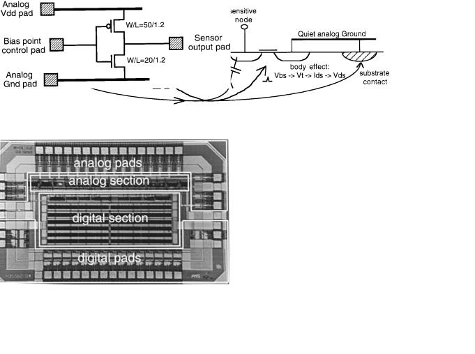
Fig. 2. Photography of the test IC designed.
III. CIRCUIT DESCRIPTION
A test circuit has been designed in a 1.2  m CMOS technology. The circuit was manufactured in two kinds of wafer: P with a typical uniform resistivity of 8.5
 cm, and P
 with a 0.7 m
 cm resistivity and a resistive epitaxial layer about 12
  m thick and with a resistivity of again 8.5
 cm. The wafer thickness is 525
  m, and a metal layer is deposited at the backside so it can act as a ground contact. Chip dimensions are 1.7
  2.7 mm
 , the periphery is formed by 18 digital input pads, 21 analog pads, and nine supply pads. The circuit is packaged in a DIL-48S, and a conductive bonding to the package backplane is done, which is wired to two grounded pins. A picture of the IC may be seen in Fig. 2.
The digital section is formed by an array of buffers with controllable activity, such that a number of buffers between 0±512 may be enabled. Buffers are driven by a clock signal of 1 MHz and 1 ns transition time. A 0.5 ns rise time and 0.4 ns fall time are estimated at the outputs of the buffers.
A simple two-transistor amplifier is used as a noise sensor, as shown in Fig. 3. The bias point of the amplifier can be controlled with the gate voltage. The output of the sensor is connected to an analog pad, and its voltage is sensed with a probe with an input impedance of 1 M


 pF. The analog section also contains some comparators for other purposes.
IV. MEASUREMENT RESULTS
A. Circuit in a Heavily-Doped Wafer (P+)
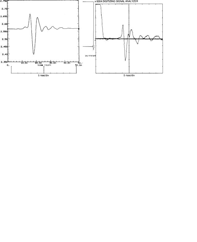
First, results of the circuit manufactured in a P wafer are presented. The typical noise waveforms obtained when
Fig. 3. Scheme of the analog sensor configuration.
the sensor amplifier is biased at the maximum gain point,


 , are shown in Fig. 4. A falling edge at the output of the switching buffers produces somewhat smaller peak-to-peak values, but the most important thing to note is that both waveforms are essentially the same. This indicates that most of the noise is introduced to the substrate from the digital power-supply lines, and not through the junctions of the switching transistors. In this second mechanism, the coupling is capacitive and produces complementary waveforms in both transients. On the contrary, noise at the digital supply lines will present the same aspect in both transitions. This is because the current through the package supply pins has the same direction for any switching of a logic gate.
Noise measurements have also been obtained when the sensing amplifier is biased at DC voltages ranging from 0±5 V. Fig 5(a) shows the measured transfer characteristic of the amplifier, while Fig. 5(b) shows the noise dependence obtained. It can be seen that noise is clearly smaller when one of the transistors is cutoff. When both transistors are ON, noise decreases slightly when decreasing the output voltage, except for an increase when placing the sensor at its high gain region.
Noise received by the sensor is the addition of contributions of the noise coupled directly from the substrate, plus the contribution of noise at power-supply lines, which will depend on the sensor bias point. If 


 V, the instant noise measured will be the average of noise at both power-supply lines, plus the noise received from the substrate. The gain of the sensor only affects the noise received from the substrate by body-effect. If the noise dependence on the gain is small, as shown in Fig. 5, this means that most of the noise is received from the supply lines. When the NMOS transistor is cutoff, the noise sensed is basically the noise present at the analog Vdd line, while if the PMOS is cutoff, the noise measured is basically that of the analog GND.
` |
1407 |
ARAGONES AND RUBIO: COMPARISON OF SUBSTRATE NOISE COUPLING |
(a) |
(b) |
Fig. 4. Noise waveforms detected with the amplifier sensor, IC manufactured in a P + wafer: (a) noise produced by the rising edge at the output of the noisy buffers and (b) noise produced by the falling edge at the output of the noisy buffers.
(a)
(a)
(b)
Fig. 5. (a) DC transfer curve of the amplifier sensor and (b) noise measured in function of the bias point of the amplifier sensor.
B. Extraction and Simulation Results
We have performed simulations of the extracted full circuit, including a model of the P substrate. The model used is that proposed in [6] and [12], in which the heavily-doped bulk behaves electrically as a single node, and the epitaxial layer is modeled as a mesh of resistances between every device and this node. Furthermore, equivalent resistances between every supply or biasing line and the substrate node across the
(b)
Fig. 6. Noise waveforms detected with the amplifier sensor, obtained from the simulations of the circuit extracted, including the resistances of the P+ substrate: (a) noise produced by the rising edge at the output of the noisy buffers and (b) noise produced by the falling edge at the output of the noisy buffers.
epilayer are also included. Resistance values are obtained from a set of device simulations. The pads include substrate contacts
1408 |
IEEE JOURNAL OF SOLID-STATE CIRCUITS, VOL. 34, NO. 10, OCTOBER 1999 |
(a) |
(b) |
Fig. 7. Noise waveforms detected with the amplifier sensor, IC manufactured in a P |
wafer: (a) noise produced by the rising edge at the output of the |
noisy buffers and (b) noise produced by the falling edge at the output of the noisy |
buffers. |
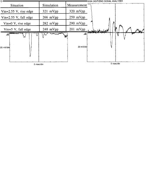
TABLE I
COMPARISON OF NOISE LEVELS MEASURED AGAINST LEVELS
OBTAINED WITH SIMULATION OF THE EXTRACTED CIRCUIT
as a single node, and coupled to the GND analog line again resistively, through the substrate contacts. The waveforms at the digital GND line, substrate node, and analog GND lines, were almost identical.
that are connected to the corresponding supply lines (analog lines if they are analog pads, digital lines for the digital pads). A package pin model consisting of an inductance, a series resistance, and a parallel capacitance [13] is used, with selfinductance values obtained from device simulation of the DIL package with RAPHAEL [14].
Simulation results show a very good matching with the experimental measurements. Fig. 6 shows the waveforms obtained from the simulations, in the same conditions as the measurements shown in Fig. 5, and the correlation may be verified. Noise levels are also coincident, as may be seen in Table I.
Concerning the path through which noise reaches the sensor, it has been verified that when each of the transistors in the amplifier is cutoff, the noise at its output is coincident with the noise at each supply line, thus confirming that this is the main mechanism through which substrate-coupled noise reaches the sensitive circuit. In order to know how noise reaches the supply lines, a number of simulations have been performed varying the values of the parasitic elements that could be significant, and thus check their role on the noise coupling. It was verified that the origin of the disturbance is switching noise at the digital power-supply lines, which is resistively coupled to the substrate through the contacts. In our particular circuit, this noise was mainly introduced by the contacts in the pads. Every digital pad is enclosed by a substrate biasing ring, thus forming a very low equivalent resistance between the ground line and the substrate. Noise is then propagated along the substrate
C. Circuit in a Lightly-Doped Wafer (P )
Measurements have also been performed on the circuits manufactured in lightly-doped substrates, thus direct comparisons of the noise behavior in both types of wafers can be done. Fig. 7 shows the typical waveform measured. It can be seen that waveforms are identical in both types of wafers, not only in this particular bias point of the sensor, but in any case. Noise levels, though, are approximately a third part of those measured in a heavily-doped wafer. It was also verified that noise waveforms were independent of the switching direction. The identical behavior in the two wafers means that the dominant coupling mechanisms are the same. It must be reminded that wafers have a backside grounded
contact, and in spite of that contact, |
the noise level in a |
P wafer is much larger than in a P |
one. Measurements |
removing the wire-bonding to the package backplane were also performed, and noise increased less than a 10%, which means that the effect of this type of contacts is small, and they cannot be considered a good technique to reduce substrate noise.
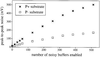
Finally, measurements in function of the activity of the digital section have been performed. Fig. 8 shows noise levels measured in the two type of wafers, for an increasing number of digital switching buffers enabled, all buffers switching synchronously. The behavior is identical in both types of wafer, a sustained increase with the number of switching gates.
V. DISCUSSION
Noise attenuation behavior depends on the type of wafer. Measurements on the test IC show that lightly-doped wafers are about three times less noisy than heavily-doped epi ones, and that the presence of a grounded backside contact has negligible influence even in a heavily-doped wafer. Given that attenuation rate in fact depends on layout and package
` |
1409 |
ARAGONES AND RUBIO: COMPARISON OF SUBSTRATE NOISE COUPLING |
Fig. 8. Noise measured in function of the activity of the digital section, in both type of wafers.
conditions, this measured relationship will not be universal, but lightly-doped wafers are clearly more advisable than heavilydoped ones for mixed-signal IC manufacturing.
It has been verified that delta-I noise at the power-supply lines is a major contributor to substrate noise. Then, a main concern should be to reduce noise at the digital supply lines down to levels much lower than those demanded by the noise margins of the digital circuitry. This may be pursued by using some of the many techniques proposed in the literature to overcome this problem [15]±[17], and also with accurate package and pin assignment selectionÐto minimize inductances of the power-supply pins. It has also been verified that noise is reduced with the number of switching gates, thus policies to partition and disable parts of the digital circuitry are encouraged.
We have shown that substrate noise is coupled to the analog circuitry mainly from the supply lines, while junctions and body-effect have a minor role. Thus interaction between these lines and the substrate should be a major concern, avoiding the use of analog lines to ground the substrate, using wells for isolation purposes, etc.
It has been shown that the pads may be the dominant place through which noise is coupled. Then, it will be useless to care about suitable substrate biasing, guard rings, etc., if interaction through the pad periphery is allowed. Only when the measures concerning delta-I noise reduction and isolation to analog supplies are achieved, will it be useful to care about guard rings and techniques to favor noise attenuation with distance.
VI. CONCLUSION
A mixed-signal test IC to measure substrate-coupled noise has been manufactured in a 1.2  m technology and in two different types of wafers. Heavily doped wafers are more noisy than lightly doped ones, and thus less advisable for mixedsignal IC manufacturing. The measurements on the test IC and simulations of the circuit including the resistive substrate have
allowed the identification of the main mechanisms through which noise is coupled in a mixed-signal IC. From this identification, a hierarchy of measures to reduce substrate noise may be established. Basic measures are those related with wafer, package and pin assignment selection. Next, the noise introduced through the IC periphery must be minimized, particularly caring for the substrate contacts in the pads. Only if these actions are undertaken, it will be sensible to add guard rings or use circuit topologies aimed to reject noise.
REFERENCES
[1]N. K. Verghese, and D. J. Allstot, ªSUBTRACT: A program for the efficient evaluation of substrate parasitics in integrated circuits,º in
Proc. IEEE Int. Conf. Computer-Aided Design, San Jose, CA, 1995, pp. 194±198.
[2]F. Clement, E. Zysman, M. Kayal, and M. Declercq, ªLAYIN: Layout inspection CAD tool dedicated to the parasitic effects through the substrate of integrated circuits,º in Proc. Power Timing Modeling Optimization Workshop, PATMOS, Oldenburg, Germany, 1995, pp. 267±276.
[3]T. Smedes, N. P. van der Meijs, and A. J. van Genderen, ªExtraction of circuit models for substrate cross-talk,º in Proc. IEEE Int. Conf. Computer-Aided Design, San Jose, CA, 1995, pp. 199±206.
[4]E. A. Vittoz, ªThe design of high-performance analog circuits on digital CMOS chips,º IEEE J. Solid-State Circuits, vol. SSC-20, pp. 655±665, June 1985.
[5]G. H. Warren, and C. Jungo, ªNoise, crosstalk and distortion in mixed analog/digital integrated circuits,º in Proc. IEEE Custom Integrated Circuits Conf., 1998, pp. 12.1.1±12.1.4.
[6]D. K. Su, M. J. Loinaz, S. Masui, and B. A. Wooley, ªExperimental results and modeling techniques for substrate noise in mixed-signal integrated circuits,º IEEE J. Solid-State Circuits, vol. 28, pp. 420±430, Apr. 1993.
[7]A. Pun, T. Yeung, J. Lau, F. R. Clement, and D. Su, ªExperimental results and simulation of substrate noise coupling via planar spiral inductor in RF IC's,º presented at the IEEE Int. Electron Devices Meeting, 1997.
[8]R. B. Merrill, W. M. Young, and K. Brehmer, ªEffect of substrate material in mixed analog/digital integrated circuits,º in Proc. IEEE Int. Electron Devices Meeting, San Francisco, CA, Dec. 1994, pp. 433±436.
[9]K. Makie-Fukuda, T. Kikuchi, T. Matsuura, and M. Hotta, ªMeasurement of digital noise in mixed-signal integrated circuits,º IEEE J. SolidState Circuits, vol. 30, pp. 87±92, Feb. 1995.
[10]T. Gabara, ªReduced ground bounce and improved latch-up suppression through substrate conduction,º IEEE J. Solid-State Circuits, vol. 23, pp. 1224±1232, Oct. 1988.
[11]J. M. Casalta, X. Aragon`es, and A. Rubio, ªSubstrate coupling evaluation in BiCMOS technology,º IEEE J. Solid-State Circuits, vol. 32, pp. 598±603, Apr. 1997.
[12]N. K. Verghese, D. J. Allstot, and M. A. Wolfe, ªVerification techniques for substrate coupling and their application to mixed-signal IC design,º IEEE J. Solid-State Circuits, vol. 31, pp. 354±365, Mar. 1996.
[13]R. Senthinathan and J. L. Prince, ªSimultaneous switching ground noise calculation for packaged CMOS devices,º IEEE J. Solid-State Circuits, vol. 26, pp. 1724±1728, Nov. 1991.
[14]RAPHAEL, ªAn interconnect analysis program,º Technology Modeling Associated Inc. (TMA), Palo Alto, CA, 1994.
[15]R. Senthinathan, J. L. Prince, and S. Nimmagadda, ªNoise immunity characteristics of CMOS receivers and effects of skewing/damping CMOS output driver switching waveform on the simultaneous switching noise,º Microelectron. J., vol. 23, no. 1, pp. 29±35, Mar. 1992.
[16]R. Senthinathan and J. L. Prince, ªApplication specific CMOS output driver circuit design techniques to reduce simultaneous switching noise,º IEEE J. Solid-State Circuits, vol. 28, pp. 1383±1388, Dec. 1993.
[17]J. L. Gonzalez´ and A. Rubio, ªTCMOS: Low noise power supply technique for digital IC's,º Electron. Lett., vol. 31, no. 6, pp. 1338±1339, Aug. 1995.