

dsd11-12 / dsd-12=Проектирование РЧ КМОП ИС / papers / 96_Verification_Techniques_for_Substrate_Coupling
.PDF354 |
IEEE JOURNAL OF SOLID-STATE CIRCUITS, VOL. 31, NO. 3, MARCH 1996 |
Verification Techniques for Substrate Coupling and Their Application to Mixed-Signal IC Design
Nishath K. Verghese, Member, IEEE, David J. Allstot, Fellow, IEEE, and Mark A. Wolfe
AbstractÐ This paper presents techniques for the analysis of substrate-coupled noise in mixed-signal integrated circuits. Advantages and limitations of some commonly employed verification techniques for substrate coupling are outlined. A preprocessed boundary element method introduced in this paper utilizes precomputed z parameters to generate an analytical model for substrate impedance in a preprocessing stage. Truncated series expansions of the analytical impedance model are used to accelerate solution of the resulting boundary element equations. A methodology that applies these fast techniques to the verification of large mixed-signal circuits and results that confirm its efficiency are described. This complete methodology has been applied to the design and verification of an industrial mixed-signal video analog-to-digital converter IC for substrate noise problems.
I. INTRODUCTION
WITH increasing speeds, shrinking IC technologies, and an emphasis on compactness in consumer electronic products, monolithic mixed-signal integrated circuits are becoming ubiquitous in the semiconductor industry. The design of these circuits is unfortunately becoming an increasingly formidable task owing to the various parasitic coupling problems that affect mixed-signal systems. The coupling of noise between the on-chip digital and analog circuits can corrupt low level analog signals and impair the performance of such mixed-signal circuits. Near field coupling between neighboring circuits and coupling between widely separated circuits through the chip substrate and power rails are the big problems. The chip substrate acts as a collector, integrator, and distributor of coupled noise on-chip. In fact, substrate coupling is one of the main reasons causing many to put analog and digital on separate IC's. For some sensitive classes of circuits, this may be the only alternative; separate IC's mounted in a multichip module, separate packages, or chip-on-board (COB) packaging. In many cases, however, the analog can be made to coexist with the switching functions. This may be at the cost
Manuscript received August 30, 1995; revised December 12, 1995. This work was supported by Texas Instruments and the Semiconductor Research Corporation under Contract 94-DC-068.
N. K. Verghese was with the SRC-CMU Research Center for ComputerAided Design, Department of Electrical and Computer Engineering, Carnegie Mellon University, Pittsburgh, PA 15213 USA. He is now with Cadence Design Systems, San Jose, CA 95134 USA.
D. J. Allstot was with the SRC-CMU Research Center for Computer-Aided Design, Department of Electrical and Computer Engineering, Carnegie Mellon University, Pittsburgh, PA 15213 USA. He is now with the Department of Electrical and Computer Engineering, Oregon State University, Corvallis, OR 97331 USA.
M. A. Wolfe is with Texas Instruments Inc., 8360 LBJ Freeway, Dallas, TX 75243 USA.
Publisher Item Identifier S 0018-9200(96)02452-3.
of strict partitioning of switching and non-switching functions, extensive special handling, a special semiconductor process, and perhaps even a fully custom design effort. Since a singlechip solution is often the smallest, lowest cost, and lowest power implementation, the additional effort is often justified. As the number of logic switching functions increases, the degree of difficulty merging the digital and analog functions will increase [1].
A primary concern of analog and mixed-signal designers today is to be able to quantify the noise coupling onto sensitive analog nodes in their designs and to effectively deal with it without the need for expensive redesign and refabrication. On the verification front, crosstalk and coupling through package and chip interconnects have been the subject of much research. Most integrated circuit designers today use parasitic RLC models of chip, package, and board level interconnects to more accurately analyze their designs for capacitive and inductive crosstalk and supply bounce. However, the simulation of noise coupling through the common substrate of mixed-signal systems has in large part been ignored, mostly due to the difficulty in dealing with analysis of the substrate itself, which is in effect a multidimensional interconnect connecting every transistor on the die with every other one. While mixed-signal designers have employed specialized models for substrate coupling in the verification of their systems [2], [3], accurate and process-independent simulation of it has only recently begun to receive attention [1], [4]±[13]. Several techniques for the analysis of substrate coupling in mixed-signal integrated circuits are examined in this paper along with their advantages and limitations.
Section II describes the underlying simplified equation that characterizes substrate behavior for substrate coupling analysis. Section III describes the numerical finite difference method that can be used to determine reduced order substrate models. Section IV describes the generalized boundary element method using Green's function to analyze substrate
coupling. Section V |
introduces a preprocessed boundary |
element method that |
utilizes precomputed parameters to |
generate a simple analytical model for substrate impedance in a preprocessing stage. A technique that uses truncated series expansions of this analytical impedance model to accelerate solution of the preprocessed boundary element equations is also discussed in Section V. Section VI outlines a methodology for substrate coupling analysis in large circuits. Section VII discusses an application of the techniques presented in this paper to the verification and design of a mixedsignal video A/D converter IC for substrate noise problems.
0018±9200/96$05.00 ã 1996 IEEE

VERGHESE et al.: VERIFICATION TECHNIQUES FOR SUBSTRATE COUPLING AND THEIR APPLICATION TO MIXED-SIGNAL IC DESIGN |
355 |
II. SIMPLIFIED SUBSTRATE EQUATION
Although semiconductor behavior can be ªaccuratelyº analyzed using a semiconductor device simulator, simplifications on the physical equations that govern it are necessary in order to allow for efficient substrate coupling analysis. The underlying strategy to verify a circuit for substrate-coupled noise is to simulate it in conjunction with a suitable substrate model using a circuit simulator or other general-purpose simulator. Since, in such a simulation environment, semiconductor devices are abstracted into multiterminal elements, it is only necessary to deal with the substrate outside the active areas.
Outside the active areas (devices and contacts) which are considered equipotential ports, the substrate can be treated as consisting of layers of uniformly doped semiconductor material of varying doping densities. In these layers, simplifications can be made on the governing semiconductor equations [12] to yield the following equation:
|
|
|
|
|
(1) |
|
|
|
|
|
|
where is the electric field intensity vector, |
and are the |
||||
sheet resistivity and dielectric constant of the semiconductor, respectively.
Equation (1) is actually a simplified form of Maxwell's equation derived by neglecting the effects of magnetic fields on-chip [12].
Equation (1) can be discretized on the substrate volume either in differential form using finite difference techniques or in integral form using boundary element methods. The discretization process leads to a large matrix representation of coupling in the substrate which can then be reduced to a simple equivalent macromodel between the defined ports in the system.
The simplified (1) for substrate coupling analysis has been verified by the authors in [7] using comparisons to device simulations and to measured results. In all subsequent discussions, it is assumed that this simplified equation is adequately accurate to simulate substrate coupling. Emphasis will be
placed instead on the |
development of |
efficient techniques |
to solve (1) for large |
problems and to |
the application of |
the solution methodology to mixed-signal IC design and verification. The interested reader is referred to our earlier work [7] for a more detailed description of the background information.
III. FINITE DIFFERENCE METHOD
In differential form, the commonly employed discretization technique for (1) is the finite difference (FD) method. With this approach, nodes are defined across the entire substrate volume and the electric field vector between adjacent nodes is approximated using a finite difference operator. Discretizing
(1) on the substrate volume results in a mesh circuit consisting of nodes interconnected by branches of resistors and capacitors in parallel, the values of which are determined from process parameters (sheet resistivity or doping density, dielectric constant) and corresponding layout geometries. The resulting RC mesh network interconnecting the ports on-chip
can then be reduced to a lower order model using a suitable moment-matching method. With the reduced order model of the substrate, it is possible to simulate for substrate coupling in a circuit using a typical circuit simulator [5].
For typical mixed-signal circuits, the intrinsic substrate capacitance can be neglected for operating speeds of up to several GHz. Designers have used the resistive substrate assumption in their modeling strategies with successful results [2], [3]. For the finite difference-based mesh model, the negligible effect of the intrinsic substrate capacitance implies that if the wells are also considered as ports which are connected to equivalent lumped well diffusion capacitances external to the mesh itself, the substrate can be considered a purely resistive mesh [7]. Since solution of the large sparse mesh matrix is done iteratively, an advantage of using this simpler resistive mesh is that network reduction of it requires fewer matrix solutions and it is therefore less computationally intensive than reducing an RC mesh using a moment-matching method. Also, the resulting reduced order resistive model consists of fewer elements and nodes (no extra nodes are needed to represent it) than a reduced order RC model. Simulation results using a purely resistive substrate model were shown to be identical to those obtained using a reduced order RC model on several representative circuit structures in [7].
Because of their applicability to virtually any type of silicon substrate, finite difference-based mesh techniques are finding increasing use in substrate modeling of integrated circuits [7], [8], [11], [14]. Being a purely numerical technique, however, it suffers from a problem all numerical discretization schemes suffer from in that the solution accuracy depends highly on the resolution of discretization. This is especially true in case of a lightly-doped substrate (i.e., any substrate without a heavilydoped bulk) without a metallized backside contact. In such substrates, a lot of empty space (between ports) must be discretized to get an accurate estimate of port-to-port substrate admittance [12]. Consequently, with increasing number of ports in the problem, the size of the resulting finite difference mesh matrix, although sparse, quickly becomes too large to solve. Alternatively, one can turn to integral methods to solve
(1).
IV. BOUNDARY ELEMENT METHOD
For the resistive substrate case, (1) reduces to the wellknown Laplace's equation
(2)
where  is the electrostatic potential. Applying Green's theorem to (2) gives the electrostatic potential at an observation point,
  , due to a unit current injected at a source point,
 , as
, as
(3)
where 


 is the substrate Green's function satisfying the boundary conditions of the substrate and


 is the source current density. Since all the source and observation points are at the defined ports on the substrate and these are planar and

356 |
IEEE JOURNAL OF SOLID-STATE CIRCUITS, VOL. 31, NO. 3, MARCH 1996 |
practically two dimensional, the volume integral of (3) reduces to a surface integral. (Note that this is only a simplifying assumption and not a restriction)
(4)
Essentially, this reduces a 3-D problem into a 2-D problem. Moreover, since the Green's function implicitly takes the substrate boundaries into account, there is no need to explicitly consider them when solving (4). This has dramatic consequences in the solution procedure since it implies that only the port areas (that actually connect to the substrate) need to be discretized to solve (4). The substrate Green's function can be determined analytically using classical mathematical techniques [16] and has been reported in literature [6], [10], [13]. Once the Green's function is determined, (4) remains to be solved. The solution is once again obtained using a suitable discretization technique. Discretizing each port on the substrate into a set of panels as shown in Fig. 1, a system of equations can be formulated that relate the currents and potentials at all panels in the system. In matrix form this is represented as
(5)
where each entry in the impedance matrix, 
 is given as
(6)
where  and
and  are the surface areas of panels
  and
and  , respectively. The impedance given by (6) can be analytically determined for rectangular panels once the Green's function is derived. The impedance matrix,
  , is then inverted to obtain the substrate admittance matrix,
  . The substrate resistance between any two ports is then obtained as the reciprocal of the sum of corresponding admittance matrix entries.
A major advantage of the boundary element method is that it is not very discretization-dependent (unlike finite differences). Although it is erroneous to assume that a port has a constant current density across it (by discretizing it into a single panel), a very coarse discretization can offer results that are within 10% of the actual answer. The computational advantage this method offers by dramatically reducing the size of the matrix to be solved (compared to the finite difference matrix) is somewhat limited by the fact that the impedance matrix to be inverted,  , is fully dense. The finite difference matrix, on the other hand, is extremely sparse, but much, much bigger! An LU factorization-based solution of the dense boundary element method (BEM) matrix is


 in matrix size and consequently infeasible for large problems. In order to accelerate the BEM solution methodology, we consider an alternate formulation of substrate impedance.
V. PREPROCESSED BOUNDARY ELEMENT METHOD
Consider |
two |
square panels on a substrate separated by |
a distance, |
, as |
shown in Fig. 2. Assume that the panels |
are equipotential and that the current density across them is uniform. The matrix equation that characterizes the interaction
Fig. 1. Discretization of a port into panels in the boundary element method. The smaller edge cells account for the singularity in current density at the port's edges.
Fig. 2. Two panels on a substrate separated by distance, d.
between the two panels is given by |
|
||
|
|
|
(7) |
Theoretically, |
is the potential |
observed at panel when |
|
a unit current is injected into panel and panel |
is floating |
||
(i.e., zero current applied to it), |
, the potential on panel |
||
due to a unit current at panel |
(with panel |
floating) and |
|


 , the potential on one (floating) panel due to a unit current injected at the other (Note that reciprocity demands that they be equal). Given a set of sizes for the two panels and ignoring the effects of the edges in the lateral plane of
the substrate, |
and |
have constant values. Moreover, the |
||||||
parameter |
depends only on the distance, |
between the |
||||||
two panels and it decreases as the distance, |
is increased. |
|||||||
Consequently, the variation of |
|
with can be characterized |
||||||
efficiently as a polynomial in |
|
|
, i.e., |
|
||||
|
|
|
|
|
|
|
|
(8) |
|
|
|
|
|
|
|
|
(9) |
|
|
|
|
|
|
|
|
(10) |
|
|
|
|
|
|
|
|
|
where the constants, 


 , and the polynomial order,
  can be determined by first precomputing the actual parameters and then using a suitable curve fitting technique. The curve fitting can be done in a preprocessing step and requires to be computed only once for a given process. The resulting polynomials can then be stored in a library and used repeatedly in the real-time extraction of (possibly different) IC's.
A. Effect of Lateral Chip Edges
An important assumption made in the formulation of the impedance model above is that the effect of the lateral chip edges can be ignored. Fig. 3 shows an experimental setup used to study the effect of the lateral chip edges on computed substrate resistance values. It consists of an output buffer cell (including bonding pad and electrostatic discharge (ESD)
VERGHESE et al.: VERIFICATION TECHNIQUES FOR SUBSTRATE COUPLING AND THEIR APPLICATION TO MIXED-SIGNAL IC DESIGN |
357 |
protection circuitry) from an industrial mixed-signal IC that is placed approximately 200  m (i.e.,


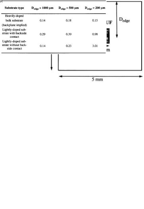
 m in Fig. 3) from the chip edge (The output buffer circuitry is typically closest in vicinity to the chip edge on IC's). A 3- D finite difference analysis is used to compute the equivalent resistive model for substrate coupling in this cell. To measure the effect of the lateral chip edge, the cell is placed at different locations (from the edges) on the IC and the resistive model reevaluated at each location. The experiment is repeated for three representative types of substrates: a heavily-doped bulk substrate, a lightly doped substrate with a backside contact, and a lightly doped substrate without a backside contact [12]. The values of the computed resistances for the cell placed at different locations on the chip (i.e., different values of

in Fig. 3) are then compared to those obtained for the cell placed at the chip center for different types of substrates. Results of the experiment are outlined in Table I where the reported error is the percentage difference in the norms of the resulting admittance matrices. An evaluation of the results indicates that the error introduced in the resistive model is different depending on the nature of the substrate. Note that a small amount of error always manifests itself due to the numerical inaccuracy in the iterative solution procedure utilized in the 3-D finite difference analysis. For a heavilydoped bulk substrate, it is clear from Table I that the lateral chip edge has no impact on the model. For the other two substrates, a small amount of error is introduced depending on vicinity to the edge. Note that beyond a certain distance from the edge, the actual error in the norm goes to zero. The results suggest that the lateral chip edges have a negligible effect on the substrate coupling process. Although results of this experiment do not address the issue of coupling through the substrate between widely separated ports, as will be seen in Section VI, coupling between two distant ports on the substrate occurs mostly through the coupling of each to the common substrate supply in its vicinity (through substrate contacts/guard rings) and to the backplane (if any). Consequently, the direct coupling between distant ports is not as significant a contributor to the substrate coupling process as the indirect coupling provided by these other paths. In developing a fast BEM solution strategy, we will make the general assumption that the lateral chip edge effects can be ignored and that substrate impedance can be modeled independently of vicinity to the edges.
B. Precomputing  Parameters
Given that the  parameters can be modeled efficiently using (8)±(10), a question that arises is how to precompute them for use in data fitting. One approach alluded to earlier is through the Green's function. At times, however, it might become imperative to use other methods to precompute the
  parameters. An advantage that the preprocessed boundary element method offers is that it allows the parameters to be precomputed in a variety of ways.
A frequently occurring problem in real IC processes is that process specifications of a substrate profile in terms of layers of uniform sheet resistivity (as required by the BEM)
Fig. 3. Experimental setup to verify effect of the lateral chip edges on computed substrate resistances.
TABLE I
PERCENTAGE ERROR IN NORM OF COMPUTED ADMITTANCE
MATRIX DUE TO LATERAL CHIP EDGE EFFECT FOR
DIFFERENT CELL LOCATIONS AND SUBSTRATE TYPES
are inaccurate. Frequently, the inaccuracies arise because of resistivity fluctuations within the process itself. Sometimes, the diffusion of impurities during the process flow could alter the process specified thickness of a layer as commonly occurs
in heavily-doped bulk type substrates where a 16 |
m epitaxial |
thickness can be reduced to nearly 7 m due |
to upward |
diffusion of boron [8]. Consequently, designers often resort to making measurements to verify parameters like resistances and capacitances. The  parameters can be measured on-chip using contacts (of sizes equal to the panel sizes desired) placed at varying distances from one another [12]. Note that the
  parameters must be measured with respect to a datum node which is the backplane in the case of substrates with a backside connect. Besides measurements, the
  parameters can also be determined using a device level simulation or a 3-D finite difference analysis.
Once the  parameters are determined, the impedance model is generated using an appropriate curve fitting technique as shown in Fig. 4. Since the variation of the
 parameter over the substrate surface cannot be adequately captured in a single polynomial, the range of separations of interest is broken down into a set of intervals. The intervals are determined

358 |
IEEE JOURNAL OF SOLID-STATE CIRCUITS, VOL. 31, NO. 3, MARCH 1996 |
Fig. 5. Polynomial impedance model for two 10 m square panels on a heavily-doped bulk substrate.
Fig. 6. Polynomial impedance model for two 10 m square panels on a lightly-doped substrate without a backplane.
Fig. 4. The impedance model generation algorithm.
using a geometric progression-like heuristic which ensures that smaller intervals are generated where the gradient of the impedance is high. For each generated interval with an initial order of INIT ORDER (typically, two), a polynomial is curve-fitted to capture the variation of impedance within the interval's lower and upper bounds of separation. The error in the fitted polynomial is then determined and if it is larger than a bound, MAXERROR (typically, 1±5%) the interval size is first reduced. If the error in the recomputed polynomial is still in excess of the error bound, the order of the polynomial is increased till either the error falls within the prescribed bound or the order falls above MAXORDER (typically, four). In case the error is exceeded, a warning is provided to the user. The computed polynomial is then stored, the interval updated, and the procedure repeated until all the intervals are completed. This process is then repeated for panels of different sizes.
C. Accuracy Comparison
Figs. 5 and 6 show the polynomial approximation to actual  parameters precomputed for different values of separation between two 10
  m square panels using Green's function for a heavily-doped bulk substrate (7
  m thick, 15
  -cm epitaxial layer on a 0.02
  -cm bulk) and a lightly-doped substrate (15
  -cm with a 3
  m thick, 2
  -cm channel stop region) without a backplane, respectively. Both substrates are assumed to be 100
  m thick. The maximum approximation error over the surface of the substrate in both cases is less than a percent of the corresponding

 parameter.
Fig. 7. A simple two port problem to illustrate resolution dependence of the different solution methods.
Fig. 7 shows a two port setup located at the center of the lightly-doped substrate without a backside contact and Table II compares the resolution dependence of the finite difference and boundary element methods for this problem. The iterative incomplete Choleski conjugate gradient (ICCG) method [15] is employed for the solution of the finite difference matrix whereas the iterative generalized minimum residual (GMRES) method [18] to be discussed later is employed for the BEM matrices. To discretize the problem for the 3-D finite difference analysis, in the vertical direction, fine grids are employed near the surface of the substrate and progressively coarser ones further away from it. Similarly, in the lateral direction, fine grids are used near and around the port locations and progressively coarser ones away from them and towards the chip edges. From prior discussion on the discretization problems of the finite difference method (particularly for lightly-doped substrates), it is not surprising that a huge matrix (labelled II in Table II) is required for accurate results. For the boundary element methods, the larger matrices of

VERGHESE et al.: VERIFICATION TECHNIQUES FOR SUBSTRATE COUPLING AND THEIR APPLICATION TO MIXED-SIGNAL IC DESIGN |
359 |
TABLE II
COMPARISON OF RESOLUTION DEPENDENCE AND CPU REQUIREMENTS OF THE DIFFERENT SOLUTION METHODS
Fig. 8. Comparison of CPU times as a function of the number of panels for LU, GMRES, and multipole-accelerated GMRES algorithms.
TABLE III
COMPARISON OF RESULTS OBTAINED USING LU, GMRES,
AND MULTIPOLE-ACCELERATED GMRES METHODS
Fig. 9. Simplified associated layout of an output buffer circuit with 8 ports defined.
Fig. 10. Equivalent RLC circuit to estimate contribution of substrate admittance coefficient to coupled noise.
Table II (labelled II) correspond to a discretization where the edge panels are chosen to be 0.1 times the size of the center panel [17] while the smaller BEM matrices (labelled I) correspond to a discretization with equisized panels. It is clear from Table II that results obtained with the smaller BEM matrix are within 10% of the actual results. Note that the major computational burden in the direct implementation of Green's function (evaluated as a double Fourier series) is in computing each entry in the fully dense BEM matrix as each one requires millions of multiplications. Using the preprocessed polynomial-based model instead, this process is greatly simplified.
D. Fast BEM Matrix Solution
Clearly, a major bottleneck in the boundary element method is the solution of the dense 

 impedance matrix. LU factorization as mentioned earlier is infeasible for more than
a few hundred panels because of its 


 operation count for a dense matrix. Alternatively, iterative methods like GMRES [18] can be employed. These methods solve the matrix
equation, |
, by minimizing the norm of the residual |
error |
at every step, , in an iterative process. The |
major cost of such an algorithm is in initially stencilling the
dense matrix |
and in each iteration, , computing the matrix |
|
vector product, |
, both of which require |
operations. |
From classical potential theory, it is well-known [19] that it is possible to avoid computing most of  and to substantially reduce the operation count of

 by using an approximation to

 , if tolerable. One such approach is through the use of multipole and local expansions [20], [21]. An advantage of determining the polynomial-based impedance model is that its multipole and local expansions can be readily determined and utilized in accelerating the matrix-vector product [12]. This approach relies on the fact that the matrix-vector product is simply a calculation of the potential on every panel in the system as a result of currents injected there. A multipole

360 |
IEEE JOURNAL OF SOLID-STATE CIRCUITS, VOL. 31, NO. 3, MARCH 1996 |
Algorithm 1. Windowing-based extraction algorithm for large circuits.
Algorithm 2. Algorithm to determine global coupling between multiple power domains.
expansion is a truncated series representation of the potential at a point distant from a given current distribution. Its dual, the local expansion, is a truncated series representation of the potential distribution at points distant from a given current injection. In determining the matrix-vector product, for every panel in the system, the potential arising from interactions with nearby panels are computed directly (i.e., by adding the product of each impedance entry by its corresponding current). By accumulating the multipole and local expansions of groups of panels, potentials due to distant interactions between panels are approximately computed and added to the contribution of nearby panels. The overall computational complexity of the matrix vector product in the GMRES algorithm can thereby be reduced to 


 [12], [20], [21].
To verify the effectiveness of the multipole-accelerated GMRES algorithm in solving the boundary element equations, results using it have been compared to those obtained with both LU factorization and the GMRES algorithm without acceleration. Fig. 8 shows a comparison of CPU times required for extraction using LU factorization, the direct GMRES algo-
Fig. 11. A mixed-signal test structure for verification.
rithm, and the GMRES algorithm with multipole acceleration, as the number of panels is increased. It is apparent from Fig. 8 that the multipole accelerated GMRES (MA GMRES) method is nearly linear in the number of panels (beyond  2000 panels) while direct GMRES varies roughly as


 and LU is


 . The last data point on the GMRES curve

VERGHESE et al.: VERIFICATION TECHNIQUES FOR SUBSTRATE COUPLING AND THEIR APPLICATION TO MIXED-SIGNAL IC DESIGN |
361 |
is an estimated value since there was inadequate memory to store the dense impedance matrix. The accuracy obtained with the multipole method is illustrated in Table III, which compares one column of the admittance matrix obtained in a multipole accelerated GMRES extraction to corresponding direct GMRES and LU extracted admittances for the simplified output buffer circuit layout of Fig. 9 on a heavily-doped bulk substrate. Note that node zero in Table III represents the heavily-doped bulk which behaves as a single node [2], [3].
VI. METHODOLOGY FOR LARGE CIRCUITS
Although the techniques outlined in the previous two sections greatly accelerate the determination of substrate parasitics, armed with them alone it is not possible to model substrate coupling in large mixed-signal integrated circuits. The premise of modeling substrate coupling on a real mixedsignal IC is not one of extracting all the substrate parasitics on the IC. Clearly, even if that information could be obtained, it would probably be of little value to a designer. However, frequently enough, designers are interested in knowing how much isolation can be obtained by placing blocks of circuitry far apart on the substrate and possibly with other irrelevant circuitry in between. The verification problem then is that of ªaccuratelyº determining coupling between these blocks without getting bogged down by the details of all the irrelevant circuitry in between.
The key to being able to solve for parasitics in large circuits is to keep their scope in mind while performing the extraction. Clearly, if a coupling coefficient in the determined substrate admittance matrix has little or no impact on the actual coupling itself, solving for it is a wasted effort to begin with. However, determining a priori what coefficients can and cannot be neglected is a challenge. Once that is known, the strategy then is the age old one of divide and conquerÐdivide the big problem into many smaller ones, each of which can then be solved independently. This is the rationale behind the commonly employed windowing technique in capacitance extraction.
It is easy to see how a windowing approach might be employed for substrate resistance extraction in heavily-doped bulk substrates or substrates with a backplane in general. From the impedance profile of Fig. 5 and the results of Table III, it is evident that for increasing separation between ports on such substrates, the coupling between them is increasingly through the backplane. Then, to model substrate coupling between ports beyond a certain separation, it is only necessary to model the coupling from each to the backplane (or bulk). For a lightly-doped substrate without a backplane, it is not apparent from Fig. 6 that a windowing strategy will work. However, in such substrates, most of the substrate current flows at the surface in the low-resistivity channel stop diffusion, since it is much more heavily-doped than the intrinsic substrate material [22]. Consequently, much of the substrate injected current is picked up by active areas, especially substrate contacts, in the vicinity of the injection point [12]. This is particularly so on such substrates since latchup concerns demand that a large number of contacts and guard rings be present on-chip.
Fig. 12. Comparison of simulated results between direct extraction and extraction with windowing for a heavily-doped bulk substrate.
Fig. 13. Comparison of simulated results between direct extraction and extraction with windowing for a lightly-doped substrate without a backplane.
Fig. 14. Circuit schematic of a comparator in the ADC using chopper-type inverter string amplifiers.
Measured results from mixed-signal IC's fabricated on bulk P- wafers confirm that most of the substrate coupling on such wafers is through the substrate power supplies, which provide the most conductive paths between active areas [1].
To develop a generally applicable windowing criterion, it is necessary to understand the significance of the substrate admittance coefficients to the coupling phenomenon itself. In a worst case scenario, a determined admittance coefficient couples all the current injected into the substrate (at a given port) onto the substrate power supply in its vicinity and the


 noise developed due to the supply inductance is then routed across the chip. A worst-case heuristic estimation of the contribution of a determined admittance coefficient to the substrate noise on-chip would be the solution of a series RLC circuit as shown in Fig. 10, with the substrate resistance damping the noise coupling from the switching diffusion (and associated capacitance) to the supply inductance. An analytical

362 |
IEEE JOURNAL OF SOLID-STATE CIRCUITS, VOL. 31, NO. 3, MARCH 1996 |
Fig. 17. Simulation results of ADC output and substrate in initial design.
Fig. 15. Measured DNL performance of initial ADC design.
Fig. 18. Simulation results of ADC output and substrate after redesign.
Fig. 16. Circuit schematic of output buffer and ESD circuitry of initial ADC design displaying some extracted substrate resistances (in ).
solution to the response, 
 of the circuit of Fig. 10 to a pulse input with finite rise time and its peak-to-peak amplitude can easily be determined [12]. Given this heuristic worst case estimate for the contribution to substrate-coupled noise of a determined admittance coupling coefficient, it is possible to develop a windowing criterion based on it as shown in Algorithm 1. Typical values for SIZE and THRESHOLD are 100
  m and 5 mV, respectively.
On lightly doped substrates without a backplane biased with multiple substrate supplies, Algorithm 1 alone will fail since it localizes the problem too much and ignores far-field coupling between the multiple power domains. A practical solution is to break the problem down into a near-field one (to compute coupling from active areas to the local substrate supply) using Algorithm 1 and then to compute far-field coupling between the multiple substrate power supply domains using Algorithm
2. By ignoring local features in each of the multiple power domains, Algorithm 2 is able to formulate and solve the farfield coupling matrix with considerably greater ease. Together, Algorithms 1 and 2 can be used to model substrate coupling in large circuits independent of the nature of the substrate or the details of the process. Fig. 11 shows a test structure used to verify the methodology for large circuits. It consists of two arrays of 12 digital blocks (inverters capacitively coupled to the substrate through 0.2 pF capacitors) on either side of two sensitive analog transistor blocks (with and without a guard ring). The distance  between the analog and digital blocks is a variable used to study the effects of separation. Each block has an associated substrate connect. The substrate connects are tied to a common substrate bias through a 30 nH lead inductance. Since the structure is small enough to be extracted directly, comparisons have been made between a direct extraction and extraction with windowing (Algorithms 1 and 2). Figs. 12 and 13 compare the simulated noise voltage at the sensitive analog node (without a guard ring) on a heavilydoped bulk substrate and a lightly-doped substrate without a backplane, respectively. In both cases, the simulation result obtained using extraction with windowing is almost identical to that obtained with direct extraction. Varying the distance,
  from 50 to 500
  m and placing a local guard ring around the analog node provide little difference to the coupled noise in both cases indicating that most of the substrate coupling is through the bulk node and substrate supply, respectively.

VERGHESE et al.: VERIFICATION TECHNIQUES FOR SUBSTRATE COUPLING AND THEIR APPLICATION TO MIXED-SIGNAL IC DESIGN |
363 |
Fig. 19. Chip microphotograph of redesigned ADC.
Even for this small problem size (418 nodes), the algorithm with windowing is almost five times faster than the direct one. Similar results are obtained using Algorithms 1 and 2 for a lightly-doped substrate without a backplane biased with multiple supplies [12].
VII. APPLICATION TO MIXED-SIGNAL IC DESIGN
The methodology for modeling substrate coupling has been applied to the verification and design of a triple eight-bit, semiflash pipelined video A/D converter product IC, the Texas Instruments TVP5700 [23] for high speed video signal processing. The TVP5700 converts luminance and chrominance composite (BY and RY) analog signals into eight digital luminance signals and four multiplexed digital chrominance signals. The eight-bit semiflash A/D's consist of one bank of 15 MSB comparators and two banks of 21 LSB comparators (each bank works off alternate cycles with the extra six comparators used for error correction). The comparators themselves are commonly used chopper-type inverter string amplifiers as shown in Fig. 14. Design of the ADC began in late 1990 and after three design/fabrication iterations, it continued to fail several specifications. Some of the key problems included sparkle code errors in its ramp response and a differential nonlinearity (DNL) error greater than  1 LSB as shown in Fig. 15. From measured results, it was apparent that there was a significant amount of substratecoupled noise in the design. The inverter string comparators shown in Fig. 14 are very susceptible to noise on the substrate. Any transients on the substrate will change the threshold voltage of the NMOS transistors, thereby changing the trip
levels of the comparators. This problem, in turn, will affect the A/D accuracy. In addition, since the conversion is done in two steps, any difference in substrate noise occurring between the time the MSB comparisons are done and the time the LSB comparisons are done can result in errors around MSB transitions. The biggest contributors to substrate noise especially around MSB transitions are the CMOS outputs.
Simulations of the design without substrate models were not able to accurately quantify the problem. In the last design iteration, it was decided that the existing design would be extracted and verified incorporating suitable substrate parasitics. Since the largest capacitances and potentially the biggest sources of noise injection to the substrate were at the 12 output buffers (eight bits for the digital luminance information and multiplexed four bit nibbles for the chrominance output), these cells were extracted at a fully detailed level. Using the windowing algorithm (Algorithm 1) around each output buffer cell, the preprocessed boundary element method was employed to determine the substrate parasitics associated with each of the 12 cells. Since the  type, heavily-doped bulk substrate is biased with a single ground line, Algorithm 2 was not employed. (Far-field coupling occurs through the bulk.) Fig. 16 shows a schematic representation of one such cell along with the ESD protection circuitry. Some significant extracted values of substrate resistance are also shown in Fig. 16 where the node, SUBSTRATE represents the backplane implied by the heavily-doped bulk. To reduce the element and node count of the substrate parasitics, simpler models (using locally equipotential substrate nodes) were extracted from the logic and comparator cells.