

dsd11-12 / dsd-12=Проектирование РЧ КМОП ИС / papers / 97_Design_Strategies_and_Decoupling_Techniques
.PDF1136 |
IEEE JOURNAL OF SOLID-STATE CIRCUITS, VOL. 32, NO. 7, JULY 1997 |
Design Strategies and Decoupling Techniques for Reducing the Effects of Electrical Interference in Mixed-Mode IC's
Mark Ingels and Michiel S. J. Steyaert
AbstractÐ A key issue in the successful integration of analog circuits is a stable analog power supply. Traditional on-chip decoupling methods exhibit transients in the supply or voltage drops and power losses. This paper introduces the RLC decoupling method that features an enhanced transient response while being especially suited for low-power, low voltage applications. Both a theoretical and a practical approach are presented together with measurement results. As the benefits of a stable local power supply can be lost by the inadequate connection of two subcircuits with relative variations on the local grounds, a differential approach of signal transfer is proposed. Furthermore, the effect of a good local decoupling can be deteriorated by substrate noise, so some attention is given to this problem too.
Index TermsÐDecoupling of systems, mixed analog-digital integrated circuits.
I. INTRODUCTION
SINGLE-CHIP integration offers many advantages such as cost reduction and yield enhancement coupled with an improvement in high-frequency performance thanks to the reduced package interconnect parasitics. Many such systems contain a noise generating digital or RF part together with sensitive analog circuitry. The noisy devices may be at the origin of electrical interference. The basis of any electrical interference problem is the noise generation. Fast current variations, whether caused by digital gates or nondifferential analog circuits, result in voltage drops over bondwire and package pin inductances [1]. A noisy power supply may disturb an analog circuit on the same supply or can propagate to further lying analog circuits. Reducing noise generation by a careful design and an adequate decoupling is a first step in the reduction of interference problems [2]. Due to noise propagation through parasitic pads and the substrate analog circuits, even those located relatively far from the noise source may be disturbed. An intelligent layout minimizing parasitic coupling and the correct placement and biasing of guard rings will further combat interference problems. Finally, the last resort to counter interference problems is the use of circuits which are highly insensitive to noise. As a general rule, differential circuits are significantly more noise resistant than their single-ended counterparts [3]. However, as these measures affect the analog circuit design, they may be harder to realize and should be anticipated in an early design stage. The successful integration of high-speed mixed-mode circuits is only possible through a well considered approach of all
these topics.
An adequate on-chip power supply decoupling is essential to limit noise generation. As demonstrated in Section IV,
Manuscript received November 20, 1996; revised January 29, 1997.
The authors are with the Dept. Elektrotechniek, Katholieke Universiteit Leuven, Afd. ESAT-MICAS, B-3001 Heverlee, Belgium.
Publisher Item Identifier S 0018-9200(97)04370-9.
a simple on-chip decoupling capacitance is inadequate in many applications due to long settling times. The traditional way to limit this settling is a resistor in the power path [4] which results in a voltage drop and power loss. This paper presents a decoupling method based on a resistance- inductance-capacitance (RLC) network in Section V. As it does not suffer from the losses, it is especially suited for low-power, low-voltage applications. After the theoretical approach of the method, practical ways of implementation are demonstrated. Finally, a test chip and measurement results are presented to support the theory. Although a stable power supply is primordial for analog circuits, their signal can be deteriorated during the transfer from one subcircuit to another due to relative variations in the local reference. To limit this, a generalized differential approach can be used as demonstrated in Section II. Hereby, the analog circuits are decoupled locally, while signal transfer is regarded as a separate problem. Finally, even with optimal local decoupling, analog signals may be deteriorated by substrate noise. Some attention is therefore given to a correct placement and biasing of guard rings in Section III.
II.THE GENERALIZED USE OF DIFFERENTIAL
STRUCTURES IN MIXED-MODE DESIGN
It is a common practice to define the ultimate voltage reference, the ground, off-chip. In high-speed applications, various techniques such as separated digital and analog power lines are used to make an on-chip ground close to the external reference. In this approach all voltages are artificially referred to the external ground, with the on-chip ground tied as close to this external reference as possible. As integrated circuits are on-chip, however, they are naturally related to the onchip ground which will never be exactly equal to the off-chip reference. It is therefore more suitable to define the reference for a circuit on-chip. An adequate decoupling will keep the local circuit power constant relative to this local reference (Section IV). Signal distortion due to limited power supply rejection ratio (PSRR) is hereby minimized. Due to fast current variations in power pads, two analog subcircuits may have a different local reference, even when they share the same analog ground pad [1], [5]. Eventually, several local references may be defined for various subsystems and decoupled locally. The transmission of the signal to another subcircuit or to the outside world can be regarded as a separate problem when using a differential approach even for voltages which are singleended at first sight. A voltage is not an absolute entity, but a difference in electric potential relative to a predetermined reference. For example, the input of a transistor is the voltage
difference |
and the unwanted bulk to source |
voltage |
|
[Fig. 1(a)]. To avoid signal disturbance |
due to |
0018±9200/97$10.00 ã 1997 IEEE
IEEE JOURNAL OF SOLID-STATE CIRCUITS, VOL. 32, NO. 7, JULY 1997 |
1137 |
(a)
(b)
Fig. 1. The use of differential circuits in mixed-mode IC's.
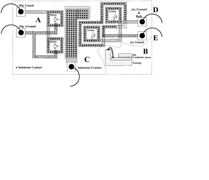
Fig. 2. Placement and biasing of guard rings.
reference variations from one place to another, voltages should be transferred concurrently with their reference through a dedicated path [Fig. 1(b)] rather than rely on a common ground. The benefit is clear from the simulation results in Fig. 1 based on an optical amplifier (stage 2) with its photodiode (stage 1). Similarly, to get the signal off chip, dedicated pins are used for the references. The relative bondwires' placement requires some attention too. Although coupling between the wires is relatively small [6], it can be sufficient to transfer noise from a noisy path to an adjacent node. Sensitive inputs' bondwires should therefore never be distant from noisy wires. Eventually they can be shielded by enclosing them with extra bondwires connected to a quiet ground.
III. PLACEMENT AND BIASING OF GUARD RINGS
Even an optimally decoupled analog circuit can be disturbed by substrate noise injected on some other place on the chip [7].
Guard rings can limit this effect when used correctly. Fig. 2 summarizes the correct placement and biasing of the rings. The first step to reduce substrate coupling is the limitation of the injected noise. A guard ring close to the digital transistors and biased with a dedicated pin will provide a return path for injected currents [Fig. 2(a)]. This ring may not be biased with either of the on-chip grounds. Biasing with the digital ground would inject extra noise into the substrate, while using the analog ground would couple substrate noise directly into it. To reduce the effect of the current which reaches the bulk, a low-impedant return path is of uttermost importance [8], [9]. For heavily doped substrates, the best result is obtained by mounting the die with conductive epoxy to the leadframe using several bondwires to connect it to the external ground [Fig. 2(b)]. Eventually, large substrate contacts with a dedicated pin filling spare places on the chip can be an alternative [Fig. 2(c)]. In lightly doped substrates where most currents flow just underneath the chip surface, a guard ring
1138 |
IEEE JOURNAL OF SOLID-STATE CIRCUITS, VOL. 32, NO. 7, JULY 1997 |
(a) |
(b) |
Fig. 3. On-chip power-to-ground impedance.
with dedicated pin surrounding the digital block is an effective return pad. In these substrates, physical separation of noise source and sensitive circuit is also very effective as the resistance in the noise path continuously increases with the distance. For heavily doped material, a separation of more than four times the epilayer thickness is useless as most of the disturbing current then just passes through the low ohmic bulk [8].
Substrate noise disturbs the analog circuits through their bulk to source voltage 


 . To reduce this bulk effect, bulksource voltage variations of analog MOS transistors should be minimized. The bulk must thus be tied locally to the analog reference rather than to the (slightly different) external one. This is achieved with bulk contacts close to the analog transistors and biased with the local analog ground [Fig. 2(d)] which results in an optimal output voltage relative to the local on-chip analog reference (Section II). A guard ring with dedicated pin around the analog circuits eventually enhances the noise immunity even further [Fig. 2(e)] [8], but does not eliminate the need of the good bulk contacts to the local analog ground.
IV. ON-CHIP POWER SUPPLY DECOUPLING
Analog circuits are disturbed by a nonconstant power supply voltage due to their finite PSRR [10]. Notice that the PSRR is related to the on-chip power to on-chip ground voltage, so an efficient decoupling minimizes on-chip power-to-ground voltage variations. Traditionally, an external capacitance was used for decoupling. This is, however, an inherent indirect approach. The off-chip decoupling capacitance keeps the offchip power-to-ground voltage constant, and it is assumed that the on-chip voltages follow it closely, so that the onchip power-to-ground voltage is constant too. This method is not suitable for high-speed integrated circuits where highfrequency current variations cause large voltage drops over the bondwire inductance. In high-speed applications, the on-chip power supply must be regulated directly and relating the onchip ground to the external reference is a distinct problem as discussed in Section II.
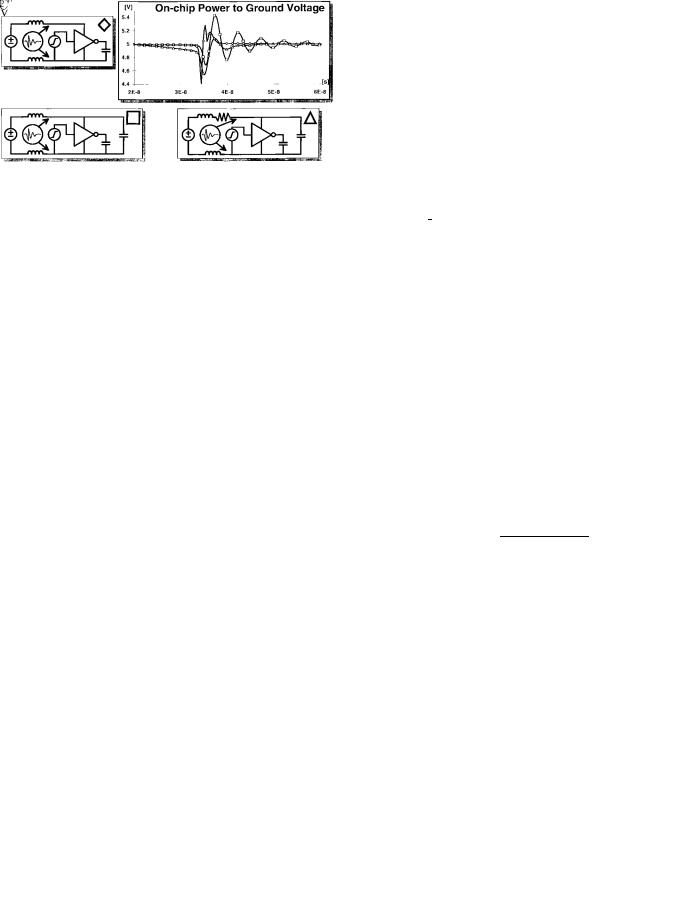
Power supply decoupling can be analyzed in the frequency domain. An integrated circuit consuming a nonconstant current generates a voltage on the on-chip power-to-ground impedance which is a combination of the bondwire inductances, the off-chip decoupling capacitor, and the total on-chip power-to- ground capacitance [Fig. 3(a)]. With no on-chip decoupling, this impedance rises with the frequency due to the bondwire inductance. To limit this impedance at high frequencies, an integrated decoupling capacitor is used. At frequencies where the bondwire impedance is noticeable, the off-chip decou-
Fig. 4. Simulation of on-chip power-to-ground voltage for some traditional decoupling methods. Inverter: 2 3 150=0:7 m and 50/0.7 m; Bondwire:
= 10 nH; Load: Cload = 5 pF; Decoupling: Cdecop = 25 pF; Q reduction: Rpower path = 15 .
pling capacitor can be considered as a shortcut. The on-chip power-to-ground impedance is then a parallel combination of the on-chip capacitance 


 and the bondwire inductance [Fig. 3(b)]. This is a resonant circuit featuring serious peaking which can also be observed in the transient response of the power-to-ground voltage. Although the maximal power supply voltage drop is reduced by the onchip decoupling capacitor, the high
  -factor causes ringing which takes a long time to extinguish [Fig. 4(b)]. This is a stringent problem in many applications. In sample-and-hold- based systems, for example, where the sampling is performed when the power supply has settled, the maximal achievable clock frequency is reduced, due to the long settling time of the power supply.
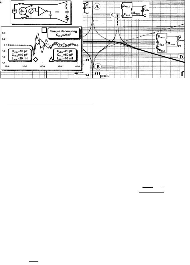
The power-to-ground impedance of an integrated circuit with on-chip decoupling capacitor is merely a parallel LC resonant circuit with resonance at [Fig. 5(a)]
(1)
To reduce the peaking and enhance the transient response, it is important to reduce the impedance's  -factor. It can be achieved by adding a resistor in series with the power supply bondwire inductance [4] [Fig. 4(c)]. This method has a major drawback: the resistor in the power path causes a voltage drop and power loss due to the dc current flowing through the power supply line. As an example, a circuit which consumes 100 mA suffers a voltage drop of 1 V and a power loss of 100 mW with a resistor of only 10
  in the power path. This corresponds to 33% power loss with a 3 V power supply. This is unacceptable in low-voltage low-power applications.
V. THE RLC-DECOUPLING METHOD
The RLC-decoupling method limits the quality factor of the on-chip power-to-ground impedance without resistor in the power path. The absence of any dc power loss or voltage drop makes this method especially well suited for low-voltage lowpower applications. The method is based on the compensation of the peak in the power-to-ground impedance frequency response [Fig. 5(a)] by the opposite peak of a serial LC resonant circuit with the same resonant frequency. With
(2)
IEEE JOURNAL OF SOLID-STATE CIRCUITS, VOL. 32, NO. 7, JULY 1997 |
1139 |
Fig. 5. On-chip power-to-ground impedance of various decoupling methods.
the power-to-ground impedance of Fig. 5(c) is given by
(3) This impedance has two new resonant peaks which are obviously as unwanted as the single decoupling capacitance peaking. By adding a resistor 

 in series with


 and
and 

 , the impedance peaking is reduced and will disappear with a correct resistor value. As this resistor is in the new serial LC-branch rather than in the power path, no voltage drop or dc power loss is introduced [Fig. 5(d)]. The RLCdecoupling circuit diagram is obviously more complex than the ªtraditionalº on-chip decoupling, but it features a largely reduced impedance peaking and consequently a much better transient response without resistor in the power path (Fig. 6). This is a major advantage in any application where the voltage drop or power loss of the simple resistor method is unacceptable. The presented technique is therefore very well suited for low-voltage low-power applications.
A. Realization of the RLC Decoupling Method
As both the resonant frequency of the original parallel LC circuit and the serial LC circuit have to coincide, 


 and
and 

 of the serial LC branch have to fulfill equation
(4)
Herein 


 is the total bondwire inductance (power and ground bondwire),

 is the total on-chip power-to- ground capacitance,


 is the total RLC inductance, and

 is the RLC decoupling capacitance. The power- to-ground capacitance

 consists of circuit capacitances, parasitic capacitances, and on-chip decoupling capacitance. The two resonant peaks of the RLC method without

 occur at
and |
(5) |
Fig. 6. Circuit diagram of the RLC decoupling method with simulated comparison to a simple on-chip decoupling capacitance.
where
(6)
with  defined in (2). With increasing
  , the two peaks move apart so that the corresponding flat impedance region resulting from the insertion of

 will span a larger frequency band. The optimal

 is achieved when the power-to-ground impedance is constant from
 to
to 
 . This optimal value decreases with increasing

 and
and  . As
. As 

 is the power- to-ground impedance of the flat region, both a large decoupling capacitance and a large
  are advantageous. An increased
  corresponds to

 getting relatively larger than


 . This certainly does not mean that the inductor should be omitted, as a zero inductance corresponds to an infinite capacitance according to (4), which is obviously infeasible.
Inductor 


 can be realized as an on-chip spiral inductor [11]. As a resistor is present in the inductor path, a very small inductor's internal resistance is not required and the spiral
1140 |
IEEE JOURNAL OF SOLID-STATE CIRCUITS, VOL. 32, NO. 7, JULY 1997 |
(a)
(b)
Fig. 7. Circuit diagram of the on-chip decoupling test chip with measurement results.
inductor can be relatively compact. A 20-nH spiral inductor will cover a chip surface of approximately (100  100)
100)  m
m . This surface corresponds to a capacitance of about 20 pF. As stated before, a large capacitor with corresponding inductor, fulfilling (4) features the best results. When the surface is limited, however, it can be interesting to replace some capacitance for inductance as the capacitance is proportional to its surface
and the inductance to its surface |
[12]. |
|
|
As |
is of the same order |
of magnitude as |
, |
a bondwire inductor can be used too [13]. This allows the use of an off-chip 

 with the connecting bondwires as inductors to enhance the on-chip decoupling. Good results can be obtained with a surface mounted device (SMD) decoupling capacitor placed in the chip package. When a short bondwire is used with a large SMD capacitor,
  can be very large, giving a flat frequency response over a large frequency range. Eventually,

 can be external to the package. It must certainly not be misinterpreted as extra off-chip decoupling which could be placed in parallel with the original off-chip decoupling capacitor. It is merely used for lowering and flattening the on-chip impedance between power and ground.
In real world situations, (4) cannot be fulfilled exactly. The smoothening of the serial RLC-peak through 

 fortunately
results in a less stringent requirement for the exact resonant frequency location. Simulations have shown that little degradation is obtained with an overestimated 

 . Therefore, to incalculate components spreading,

 should always be equal to or larger than the ideal value despite process variations. A feature of the RLC method is its ability to fix some decoupling problems in already processed IC's. Chips which do not perform according to the specifications due to ringing on the internal power supply can be fixed by adding an extra bondwire on the power and ground bondpad of the noisy power supply and use this wire as inductor in the serial RLC branch. An ªRLCº capacitor and resistor are added externally. As this implies nonstandard packaging, it is merely applicable for prototypes.
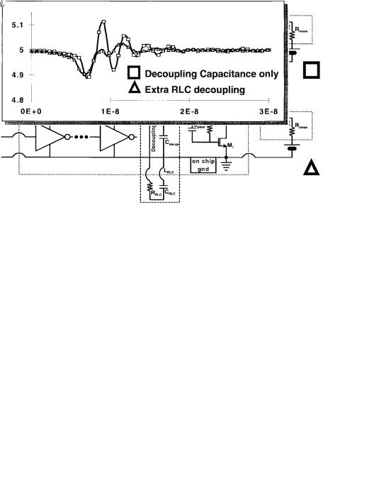
B. Test Chip and Measurement Results
A test chip has been realized to check the presented RLC method and compare it with traditional decoupling. The chip consists of several large inverter strings representing a noisy circuit which can be triggered externally or used as a ring oscillator (Fig. 7). Each string is decoupled in a different way. Herein, the RLC method is implemented with bondwire

IEEE JOURNAL OF SOLID-STATE CIRCUITS, VOL. 32, NO. 7, JULY 1997 |
1141 |
inductors. To measure the on-chip power-to-ground voltage, a differential amplifier is implemented for each stage. The variations of the supply voltage relative to the local on-
chip ground |
is passed through |
to . This |
voltage |
is converted |
into a current which flows through |
, the |
|
50- input of a scope which thus measures the local relative variation of power-to-ground on chip.
In Fig. 7 the measured on-chip power-to-ground voltage of a traditional decoupling capacitance and the RLC scheme are compared. The RLC method yields the lowest peak-to- peak voltage and shortest ringing as expected and this without resistors in the dc power path. Although the measurement is based on a digital noise source, the method is also applicable for analog circuits consuming a nonconstant current.
VI. CONCLUSION
On-chip decoupling is an important issue in mixed-mode design. Unfortunately, the simple on-chip decoupling capacitance suffers from a bad response due to its resonant behavior. The traditional remedy to this problem using a resistor in the power path introduces a voltage drop and some power loss (Section IV). This paper presented the RLC decoupling which was introduced in Section V. It features an improved transient response and is especially suited for low-power, low-voltage applications. Both the theoretical and practical implementations were exposed and measurement results were given. As the benefits of the local decoupling can be defeated during signal transfer, attention was given to a generalized differential approach to couple various subcircuits in Section II. Finally, as analog signals may be deteriorated by substrate noise even
when optimally decoupled, the correct placement and biasing of guard rings was summarized in Section III.
REFERENCES
[1]A. J. Rainal, ªEliminating inductive noise of external chip interconnections,º IEEE J. Solid-State Circuits, vol. 29, pp. 126±129, Feb. 1994.
[2]J. Williams, ªCorrecting power-supply problems,º EDN, pp. 181±190, Oct. 10, 1991.
[3]K. Makie-Fukuda, T. Kikuchi, T. Matsuura, and M. Hotta, ªMeasurement of digital noise in mixed-signal integrated circuits,º IEEE J. Solid-State Circuits, vol. 30, pp. 87±92, Feb. 1995.
[4]W. Groeneveld, ªGroundbounce in CMOS,º in Proc. AACD, Apr. 1993.
[5]Y.-I. S. Shin, ªMaintain signal integrity at high digital speeds,º Electron. Design, pp. 77±90, May 14, 1992.
[6]L. J. Giacoletto, Electronics Designers' Handbook. New York: McGraw-Hill, pp. 3.42±3.49, 1977.
[7]L. Gal, ªOn-chip cross talk±-The new signal integrity challenge,º in Proc. CICC, 1995, pp. 251±254.
[8]D. K. Su, M. J. Loinaz, S. Masui, and B. A. Wooley, ªExperimental results and modeling techniques for substrate noise in mixed-signal integrated circuits,º IEEE J. Solid-State Circuits, vol. 28, pp. 420±428, Apr. 1993.
[9]R. Gharpurey and R. G. Meyer, ªModeling and analysis of substrate coupling in integrated circuits,º IEEE J. Solid-State Circuits, vol. 31, pp. 344±353 Mar. 1996.
[10]K. R. Laker and W. M. C. Sansen, Design of Analog Integrated Circuits and Systems. New York: McGraw-Hill, pp. 562±574, 1994.
[11]H. M. Greenhouse, ªDesign of planar rectangular microelectronic inductors,º IEEE Trans. Parts, Hybrids, Packag., vol. PHP-10, pp. 101±109, June 1974.
[12]J. Crols, P. Kinget, J. Craninckx, and M. Steyaert, ªAn analytical model of planar inductors on lowly doped silicon substrates for high frequency analog design up to 3 GHz,º presented at Symp. VLSI Circuits, June 1996.
[13]J. Craninckx and M. S. J. Steyaert, ªA 1.8-GHz CMOS low-phase- noise voltage-controlled oscillator with prescaler,º IEEE J. Solid-State Circuits, vol. 30, pp. 1474±1482, Dec. 1995.