

dsd11-12 / dsd-12=Проектирование РЧ КМОП ИС / papers / 98_Substrate_Noise_Coupling
.PDFIEEE JOURNAL OF SOLID-STATE CIRCUITS, VOL. 33, NO. 6, JUNE 1998 |
877 |
Substrate Noise Coupling Through
Planar Spiral Inductor
Alan L. L. Pun, Student Member, IEEE, Tony Yeung, Student Member, IEEE, Jack Lau, Member, IEEE,
Fran¸cois J. R. Cl´ement, Member, IEEE, and David K. Su, Member, IEEE
AbstractÐWhile previous studies on substrate coupling focused mostly on noise induced through drain-bulk capacitance, substrate coupling from planar spiral inductors at radio frequency (RF) via the oxide capacitance has not been reported. This paper presents the experimental and simulation results of substrate noise induced through planar inductors. Experimental and simulation results reveal that isolation between inductor and noise sensor is less than 30 dB at 1 GHz. Separation by distance reduces coupling by less than 2 dB in most practical cases. Practical examples reveal an obstacle in integrating RF tunedgain amplifier with sensitive RF receiver circuits on the same die. Simulation results indicate that hollow inductors have advantages not only in having a higher self-resonant frequency, but also in reducing substrate noise as compared to conventional inductors. The effectiveness of using broken guard ring in reducing inductor induced substrate noise is also examined.
Index TermsÐCoupling, cross-talk, guard ring, hollow inductor, isolation, RF power amplifier, spiral inductor, substrate noise.
I. INTRODUCTION
IN THE PAST few years, we have witnessed an increasing interest in integrating inductors in analog radio frequency (RF) chips [1]. Thanks to great advances in multilayer metal processing and a higher frequency requirement, we have been able to integrate inductors of reasonable qualities. The trend to attain higher integration for lower cost is global and incessant. In a relatively small place like Hong Kong, which has a population of over 6 million, the number of cellular phones has exceeded 2 million in the year 1997 and continues to
grow rapidly.
An unfortunate byproduct of higher integration is a higher susceptibility to interference. One such interference is substrate noise. Most of the reports [2]±[4] on substrate noise have been done at lower frequencies or have been done on nonepitaxial wafers. In addition, the studies were mainly done on noise generation via junction capacitance. In this paper, we focus on the potential of substrate noise induction through spiral inductors.
Manuscript received August 19, 1997; revised December 5, 1997. This work was supported in part by the Hong Kong Government Research Grant Council.
A. L. L. Pun was with the Department of Electrical and Electronic Engineering, The Hong Kong University of Science & Techhnology, Hong Kong, China. He is now with Pencom Semiconductor, San Jose, CA USA.
T. Yeung and J. Lau are with the Department of Electrical and Electronic Engineering, The Hong Kong University of Science & Techhnology, Hong Kong, China.
F. J. R. Clement´ is with the Swiss Federal Institute of Technology, Lausanne, Switzerland and Snake Technologies, France.
D. K. Lu is with Hewlett-Packard Laboratories, Palo Alto, CA USA. Publisher Item Identifier S 0018-9200(98)03507-0.
In today's RF circuits, inductors of value in the range of nanohenrys are found [5]±[7]. Typical applications of inductors include impedance transformation, inductive degeneration, and frequency-tuned loading. The basic inductance value can be determined either analytically, based on a popular theorem proposed by Greenhouse [8], or numerically, based on some electromagnetic (EM) finite-element simulators. Typically, the size of the inductors is on the order of a few hundred micrometers by a few hundred micrometers.
For a triple-layer metal process, the inductors usually reside on roughly 3±4  m of oxide. As a result, an inductor will have a capacitance on the order of picofarads between itself and the substrate. Perturbation on the inductors will transduce noisy current in the substrate. Intuitively, the substrate noise problem will be more severe in this case as compared to that in a mixed-signal integrated circuit. In the first place, integrated inductors are required to operate in the gigahertz range, while most digital circuits operate at an order of magnitude lower in frequency. Second, in a mixed-signal case, the substrate noise is induced through the drain-bulk junction capacitance. In a typical submicron technology with a substrate doping
of |
4 |
10 cm , the drain-bulk capacitance is about 0.7 |
fF/ |
m |
. Therefore, it will take a very wide digital transistor to |
deliver the same amount of substrate noise. The difference is more prominent if one considers the fact that wide transistors are mostly used as drivers in digital VLSI and will not be running at high speed.
Section II describes the test chip and the experimental setup in detail. We also introduce a simulation technique in Section III, which can model the substrate effect and generate a lumped model for noise simulation. Section IV provides some results to verify the proposition of inductor-induced substrate noise. In Section V, we provide data on practical substrate noise impact by using the inductors as a tuned-gain stage in RF amplifier. Various methods in reducing substrate noise are also discussed in Section VI.
II. EXPERIMENTAL SETUP
A 2 mm  2 mm test chip was fabricated in a 0.8-
 m triplelayer metal CMOS n-well technology to study the substrate noise coupling effect from spiral inductors. Five three-turn inductors, each of size 350
  m
m  350
350  m using top-layer metal, are shown in Fig. 1. In addition, ten
 diffusion substrate contacts at different locations act as noise sensor for measuring noise. Each of these
 diffusion contacts is 50
  m
m  50
50  m. Dummy contacts without
 diffusion are used to calibrate out the nonsubstrate noise.
0018±9200/98$10.00 ã 1998 IEEE

878
Fig. 1. Microphotograph of the test chip.
Fig. 2. Measurement setup and cross section of the substrate.
IEEE JOURNAL OF SOLID-STATE CIRCUITS, VOL. 33, NO. 6, JUNE 1998
Fig. 3. Process flow of substrate noise simulation tools.
the ground. 
 diffusion contacts were connected to port 2 of the analyzer. As we excite the inductor, the
 parameter indicates the isolation between the inductor (noise source) and
 substrate contact (sensor). Before any measurements were taken, standard TRL calibration was done.
Studies in the past [3] have indicated that 
 diffusion guard rings are the most effective shield against substrate noise in a conventional CMOS technology. We are interested in studying the efficiency of these guard rings in our setup. Besides the peripheral guard ring that surrounds the die, a second set of guard ring surrounds two of the inductors. These guard rings are placed 175
  m from the center of the inductors. The inductor guard rings are a 25-
 m-wide diffusion region with a dedicated biasing pad. The
 diffusion ring surrounding the chip is 50
  m wide and is connected to eight bonding pads. For ease of study, the distance between
 diffusion contact and the center of inductor is defined as
  .
.  is defined as the distance from the edge of inductor guard ring to the center of inductor.
III. SIMULATION METHODOLOGY
The cross section of the basic test structure and the measurement setup are shown in Fig. 2. There is a roughly 1- m-thick
 channel stop implant of 1
 cm resistivity near the surface of the chip. The
 region with a resistivity of about 22
 cm is found transversing 8
  m into the wafer. As we transverse deeper into the wafer, the resistivity becomes less because of higher doping concentration. Eventually, the resistivity drops to 0.02
 cm and flattens out.
One of the test chips is mounted on a two-sided 31-mil- thin copper board using conductive epoxy to tie the backside of substrate to ground. In real IC, perfect grounding is not possible because of lead inductance. To study the worst case condition, another chip is mounted using nonconductive epoxy. Measurement with and without substrate tied to ground via 
 guard rings are both performed. The top side of the PCB has 50-
 lines connected to SMA connectors, while the bottom side acts as a ground plane. Unused area of the PCB is connected to the ground plane via through-holes to avoid board-level noise.
In the experiment,  -parameters were measured using an HP8753D two-port network analyzer. One end of the inductor was connected to port 1 and another end was connected to
Precise modeling of the substrate noise is often difficult due to the distributive nature of the substrate and the particulars of a specific layout. In order to have a better understanding of the substrate noise propagation, a two-step approach is used to simulate the substrate noise. As it will be shown later, the establishment of the methodology enables us to explore various noise reduction schemes.
A process flow of the substrate noise simulation is shown in Fig. 3. In the first step, physical layout is processed through a three-dimensional electrical element extractor [9]. The program is based on the finite difference method.
The layout defines the surface mesh while the vertical doping profiles of the technology determines the mesh from the top to the bottom of the wafer. The technology description includes information such as mean doping, as well as vertical and lateral resistivity for each combination of the drawn layers and for each subdivision of the mesh. Information of the doping profile of the MOSIS 0.8-  m CMOS technology with epitaxial layer on top of a heavily doped bulk was obtained using spreading resistance analysis. The result shown in Fig. 4 is the resistivity and carrier concentration along the depth of the substrate.

PUN et al.: SUBSTRATE NOISE COUPLING THROUGH PLANAR SPIRAL INDUCTOR |
879 |
Fig. 4. Doping profile of the substrate from spreading resistance analysis.
In the second step of the process, the extracted electrical
model is passed to HSPICE through which noise simulation Fig. 5. Measurement of S21 versus frequency at d = 1200 m. can be carried out.
The two-step approach has been used to study lowerfrequency substrate noise on a uniform lightly doped substrate in a 2- m CMOS technology in an earlier work [4]. It provides an easy and fast way to understand the substrate noise propagation. The program is valid for signals with periods greater than the RC time constant of the substrate. The inverse of the RC time constant is greater than 10 GHz. Details will be explained in the Appendix.
IV. MEASUREMENT RESULTS |
|
A. Effect of Operating Frequency |
|
parameters from the inductor to the |
diffusion |
contacts are measured and simulated. The distance between the edge of the inductor and the diffusion contact is 1200  m. The large distance is chosen to guarantee the substrate noise has no distance dependence.
The frequency is swept from 30 kHz to 3 GHz. Data are collected in two different configurations. In the first case, all bonding pads of the peripheral guard ring were connected to ground. In the second case, all bonding pads of the peripheral guard ring were floated without any connection. In both cases, we use either conductive or nonconductive epoxy for substrate backside contact. So, there is a total of four experiments.
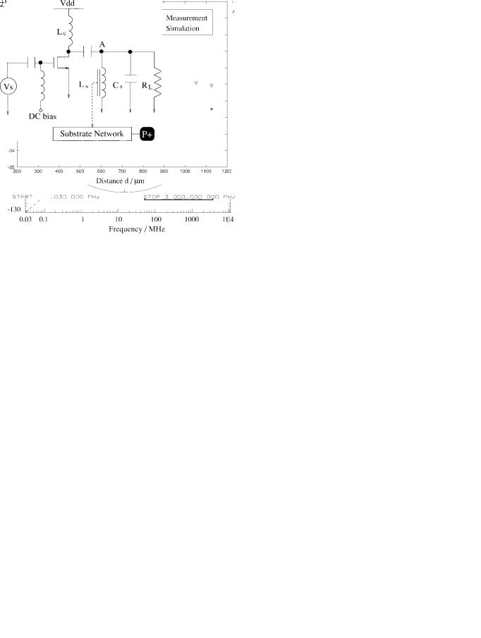
1) Low Frequency: Fig. 5 shows the measured 
 for the four different configurations. The worst case occurs with nonconductive epoxy and guard ring floated. With either guard ring grounded or backside tied to grounded, the coupling reduces by some 25 dB at frequency below 1 GHz.
It can be observed that noise coupling increases by 20 dB per decade of frequency, indicating that the coupling is mostly due to 
 . While the exact details of the distributive nature of the substrate are hard to picture, a rough equivalent circuit
can elucidate the idea (Fig. 6) [1], [10]. In the test, |
helps |
|
create a dominant zero. The value of |
in this case is about |
|
1 pF for a 4- m-thick oxideÐfar greater than that contributed by the substrate capacitance
 and
and 
 . In order to verify
Fig. 6. Equivalent lumped element circuit of the experiment setup.
this fact, after extracting the substrate resistive mesh, we backcalculated the associated substrate capacitance for each resistor grid. We resimulated with and without the substrate capacitance and observed no change in the substrate noise.
2) High Frequency: At frequency above 1 GHz, the 
 increases greater than 20 dB per decade of frequency, indicating there is another pole besides
 . This effect can be understood by comparing measured and simulated results. For ease of comparison, the measurement results are reproduced in Fig. 7 along with the simulation results for peripheral guard ring grounded and floated with nonconductive epoxy. In the simulation, we model the bond wire connected to the guard ring as a 2-nH inductor. As frequency increases above 1 GHz, the guard rings become less effective in reducing noise due to the parasitic inductance in the setup for the case of grounded peripheral guard ring. However, no parasitic inductance is involved for the case of peripheral guard ring floated with nonconductive epoxy, and thus
 continues to increase by 20 dB per decade for all frequency range.
880 |
IEEE JOURNAL OF SOLID-STATE CIRCUITS, VOL. 33, NO. 6, JUNE 1998 |
Fig. 9. Measurement and simulation of S21 versus distance d with the peripheral guard ring floated and frequency = 500 MHz.
Fig. 7. Measurement and simulation of S21 versus frequency at d = 1200m for peripheral guard ring floated and grounded with nonconductive epoxy.
Fig. 10. Schematic of power amplifier for inductor (Ls) substrate noise analysis.
Fig. 8. Measured inductor self-resonant frequency for peripheral guard ring floated (marker 1) and grounded (marker 2).
It should be pointed out that the inductor self-resonant frequency1 drops greater than 40% when the guard ring is grounded because the effective capacitance to ground is bigger. Fig. 8 shows the measured 

 which indicates the inductor self-resonant frequencies are 2.9 and 1.69 GHz for peripheral guard ring floated and grounded, respectively.
B. Effect of Physical Separation
The distance away from the inductor is in general irrelevant, as illustrated in Fig. 9. The variation of 
 is less than 2 dB
1 The self-resonant frequency means the lowest frequency such that the inductance drops to zero on the Smith chart.
as distance separation changes from 200  m to 1200
  m. The size of the inductors is quite large and certainly greater than four times the distance of the thickness of epitaxial layer. In an earlier work [2], it has been shown that substrate noise at a distance less than four times the epitaxial thickness depends on the actual distance, beyond which the epitaxial layer becomes an equal-potential node. As an interesting note, for lightly doped wafers, the dependence on distance arises when the separation is less than the wafer thickness.
V. DESIGN CONSIDERATIONS
The inductor substrate model derived above can be used to predict the inductor induced noise coupling from a narrowband tuned amplifier, a key building block for RF power amplifier is shown in Fig. 10.
In the simulation, the size of the NMOS is chosen to be
|
|
. The |
is a 3.3- |
H off-chip inductor acting as an |
|
|
|
||||
RF choke. The output load |
is 50 . The on-chip inductor |
||||
|
|
7 nH resonates with |
capacitor |
10 pF at 600 |
|
MHz. The |
substrate is connected to the |
contact via |
|||
the substrate equivalent network.

PUN et al.: SUBSTRATE NOISE COUPLING THROUGH PLANAR SPIRAL INDUCTOR |
881 |
Fig. 11. Transient analysis of noise coupling from the power amplifier inductor (Ls) to P + at d = 300 m.
Fig. 12. FFT analysis of noise coupling from the power amplifier inductor (Ls) to P + at d = 300 m.
With a power supply Vdd of 5 V, an amplifier in class- B operation can have a maximum output voltage as large as 10 V. This large output voltage across inductor  can induce a significant amount of noise in the substrate. Transient
simulation results of noise coupling from |
to a substrate |
|
contact at |
300 m are shown in Fig. 11. The noise voltage |
|
at the |
diffusion contact is about 130 |
mVpp with a 45 of |
phase shift. The corresponding fast Fourier transform (FFT)
analysis shown in Fig. 12 indicates an isolation of |
40 dB at |
the fundamental frequency. |
|
Fig. 13 shows the noise coupling from inductor |
to the |

 substrate contact increases at higher harmonic frequencies. These results show that inductor-induced noise can be a major obstacle to integrating an RF power amplifier with sensitive RF receiver circuits on the same die.
VI. VARIOUS METHODS IN REDUCING
INDUCTOR-INDUCED SUBSTRATE NOISE
A. Conventional Inductor
Fig. 13. Isolation between the power amplifier inductor (Ls) to P + at d = 300 m.
The amount of substrate noise that can be reduced by a guard ring surrounding the inductor depends on the distance from the inductor. One can view the inductor substrate capacitance as a massively parallel array of capacitors. Due to the large inductor size and the four times epi thickness requirement, an optimal guard ring placement for minimum noise can be determined. Unfortunately, as the guard ring encroaches into the inductor, the mirror effect degrades the inductance value.
An EM field simulator [11] is used to detect the inductance reduction as a function of guard ring distance. An inductor
of five turns with an outer dimension of 180 m |
180 m, a |
line width of 15 m, a turn-to-turn spacing of 1 |
m, and metal |
(aluminum) thickness of 1.2  m is simulated to be about 2 nH
under free space. The corresponding capacitance  is about 0.28 pF and the self-resonant frequency is 6.7 GHz. Fig. 14 shows the simulation results of inductance, together with
 versus
  under the conditions of
 300
300  m and frequency of 1 GHz, where
  is defined as the distance from the center of the inductor to the edge of the guard ring, and
  is the distance from the
 diffusion contact to the center of the inductor. With the guard ring grounded, the inductance value decreases dramatically as the guard ring moves inward into the inductor. The effect of the guard ring becomes void as it approaches the center of the inductor. Both the inductance value and noise coupling show no change. As the guard ring is placed far away from the inductor, the mirror effect is almost nonexistent and the inductance reduces by only 10%. Yet, the

882 |
IEEE JOURNAL OF SOLID-STATE CIRCUITS, VOL. 33, NO. 6, JUNE 1998 |
TABLE I
COMPARISONS OF CONVENTIONAL AND HOLLOW INDUCTOR
Fig. 14. Simulation results of inductance and S21 for solid inductor at d = 300 m. Five-turns 2-nH inductor of size 180 m 2180 m.
Fig. 16. Broken inductor guard ring at r = 175 m.
Fig. 15. Simulation results of inductance and S21 for hollow inductor at
d= 300 m. Two-turns 2-nH inductor of size 260 m 2260 m.
noise can be reduced to a reasonable level with the guard ring grounded.
B. Hollow Inductor
It has been understood that the magnitude of coupled noise is directly proportional to the value of oxide capacitance. However, we cannot change the oxide thickness as a way to reduce  for a given fabrication process.
A hollow inductor has been proven [12] to have a higher quality factor and self-resonant frequency for the same value of inductance as compared to conventional inductor. We are interested to know if the hollow inductor has any advantage as far as substrate noise is concerned. A two-turn hollow inductor with an outer dimension of 260  m
m  260
260  m is simulated to be about 2 nHÐthe same as that in the conventional inductor. The other dimensions of inductor are the same as the conventional inductor. The corresponding capacitance
is about 0.127 pF which yields a self-resonant frequency of
about 10 GHz. Results illustrated in Fig. 15 indicate that noise is about 7±12 dB less in the hollow case as compared to that in the conventional one. However, there are tradeoffs for the minimum inductance drops to about 25% of the original value.
A comparison between a conventional inductor and the hollow inductor is tabulated in Table I. The capacitance  of the conventional inductor is bigger than the hollow one with the same value of original inductance. Thus, higher selfresonant frequency can be achieved for thehollow inductor. The smaller
  also implies smaller substrate noise in the hollow inductor. The smaller minimum inductance happened in the hollow case when the guard ring is placed underneath the inductor.
C. Discontinuous Guard Ring
As the guard ring is placed near the inductor, the mirror effect becomes a serious problem as it reduces the original designed inductance value dramatically. In order to reduce the eddy current that flows in the substrate, a broken guard ring is employed. Fig. 16 shows the broken guard ring setup with a width of 25  m placed near the edge of the inductor. The
 substrate contact is set at a distance of 450
  m from the center of inductor. The original inductance value is about 2 nH. Simulation results shown in Fig. 17 reveal that the halfbroken guard ring (50% area) reduces noise significantly while the inductance drops by only 8%.
PUN et al.: SUBSTRATE NOISE COUPLING THROUGH PLANAR SPIRAL INDUCTOR |
883 |
Fig. 17. Simulation results of inductance and S21 for broken guard ring, which is specified as area % of the complete ring.
Fig. 18. Model for a piece of homogeneous substrate.
VII. CONCLUSION
The experimental results and simulation verifications provide an understanding of the noise coupling effect of planar spiral inductor in a heavily doped silicon substrate. It would be a major obstacle to integrate an RF power amplifier with a sensitive RF receiver circuit on the same die. Simulation reveals that a hollow inductor has advantages in reducing inductor induced substrate noise as compared to conventional inductor. A broken guard ring can help reduce the substrate eddy current induced by the inductor and hence reduce noise while maintaining the inductance value.
APPENDIX
Capacitive and resistive effects occur throughout the sub-
strate. Inside a doped |
semiconductor, the conductivity |
is |
||
given by |
|
, where |
is the electronic charge, |
|
and |
represent the mobility of |
- and -carriers, and |
||
and |
stand for the |
- and -carrier density, respectively. |
||
Therefore, the current |
density is given by (1), where |
is |
||
define as the electric field |
|
|
||
|
|
|
|
(1) |
The  and
and  parameters vary as functions of the total semiconductor doping and temperature.
In the frequency domain, the equivalent admittance  for a piece of substrate as illustrated in Fig. 18 is given by
(2)
where  is defined as the substrate time constant
(3)
For low frequencies, substrate resistance  is more important, and the associated capacitance
  can be neglected. As frequency
  increases, the capacitive effect rises to become equal to the resistive effect at the cutoff frequency
  defined by
(4)
The minimum  is attained for a lightly doped
  -type substrate because mobility is lower for holes than for electrons. The extreme case of a normal initial carrier concentration of 10
 cm
cm
 yields a minimum cutoff frequency given by
(5)
The minimum cutoff frequency is greater than 10 GHz for

 480 cm
 /Vs at temperature of 300 K. At higher doping concentration, such as that in the highly conductive substrate in an epi-process (
 10
10
 cm
cm
 ), the cutoff frequency is an order of magnitude higher.
Therefore, the capacitance of the substrate can be neglected in the lower RF range for substrates doped homogeneously.
ACKNOWLEDGMENT
The authors would like to thank their colleagues and technical staffs in the Department of the Electrical and Electronic Engineering at The Hong Kong University of Science & Techhnology for their kind help, invaluable suggestions, and technical assistance. In particular, they thank L. Tsui, F. Hui, and Z. Chen in the Consumer Media Laboratory; S. F. Luk in the VLSI Laboratory; P. H. Yin and C. Y. Wong in the Wireless Communication Laboratory; P. Chan in the Analog Laboratory; and A. Ng in the Device Characteristics Laboratory. A special acknowledgment is extended to Y. K. Leung and Prof. S. Wong at the Center for Integrated Systems at Stanford University for providing spreading resistance analysis. The useful comments of the reviewers have also been noted.
REFERENCES
[1]K. B. Ashby, I. A. Koullias, W. C. Finley, J. J. Bastek, and S. Moinian, ªHigh Q inductor for wireless applications in a complementary silicon bipolar process,º IEEE J. Solid-State Circuits, vol. 31, pp. 4±9, Jan. 1996.
[2]D. K. Su, M. J. Loinaz, S. Masui, and B. A. Wooley, ªExperimental results and modeling techniques for substrate noise in mixed-signal integrated circuits,º IEEE J. Solid-State Circuits, vol. 28, pp. 420±430, Apr. 1993.
[3]K. Joarder, ªA simple approach to modeling cross-talk in integrated circuits,º IEEE J. Solid-State Circuits, vol. 29, pp. 1212±1219, Oct. 1994.

884
[4]T. Blalack, J. Lau, F. J. R. Clement, and B. A. Wooley, ªExperimental results and modeling of noise coupling in a lightly doped substrate,º in
Proc. IEEE Int. Electron Devices Meet., 1996.
[5]D. K. Shaeffer and T. H. Lee, ªA 1.5 V, 1.5-GHz CMOS low noise amplifier,º IEEE J. Solid-State Circuits, vol. 32, pp. 745±759, May 1997.
[6]N. M. Nguyen and R. G. Meyer, ªA Si bipolar monolithic RF bandpass amplifier,º IEEE J. Solid-State Circuits, vol. 27, pp. 123±127, Jan. 1992.
[7]M. Soyuer, K. A. Jenkins, J. N. Burghartz, H. A. Ainspan, F. J. Canora, S. Ponnapalli, J. F. Ewen, and W. E. Pence, ªA 2.4 GHz silicon bipolar oscillator with integrated resonator,º IEEE J. Solid-State Circuits, vol. 31, pp. 268±270, Feb. 1996.
[8]H. M. Greenhouse, ªDesign of planar rectangular microelectronic inductors,º IEEE Trans. Parts, Hybrids, Packaging, vol. 10, pp. 101±109, June 1974.
[9]F. J. R. Clement, E. Zysman, M. Kayal, and M. Declercq, ªLAYIN: LAYout inspection CAD tool dedicated to the parasitic coupling effects through the substrate of integrated circuits,º Power and Timing Modeling Optimization and Simulation, 1995.
[10]C. P. Yue, C. Ryu, J. Lau, T. H. Lee, and S. S. Wong, ªA physical model for planar spiral inductors on silicon,º in Proc. IEEE Int. Electron Devices Meet., 1996.
[11], Maxwell Quick 3D Parameter Extractor User's Reference, An-
soft Corp.
[12]J. Craninckx and M. Steyaert, ªA 1.8 GHz low-phase-noise CMOS VCO using optimized hollow spiral inductors,º IEEE J. Solid-State Circuits, vol. 32, pp. 736±744, May 1997.
IEEE JOURNAL OF SOLID-STATE CIRCUITS, VOL. 33, NO. 6, JUNE 1998
Jack Lau (S'89±M'90) received the B.S. and M.S. degrees in electrical engineering from the University of California at Berkeley. He received the Ph.D. degree at the Hong Kong University of Science & Technology in 1994. His M.S. thesis involved the design and analysis of integrated pin drivers for incircuit testing.
While at Berkeley, he worked at Hewlett-Packard as a Technical Support Intern and at Schlumberger as an Automatic Test Equipment Engineer. After receiving the M.S. degree, he worked as a CPU
Design Engineer at Integrated Information Technology Santa Clara, CA. His Ph.D. thesis at the HKUST is on integrated silicon magnetic sensor. From 1995 to 96, he was a Visiting Scholar at Center for Integrated Systems at Stanford University researching in RF CMOS circuits and substrate noise coupling issues. His research interests are in analog high-frequency IC design for wireless applications and integrated magnetic sensor.
Dr. Lau is a recipient of the UC Berkeley Alumni Scholarship, Cray Research Scholarship, and Unisys Scholarship. He is also the recipient of the 1995 School of Engineering Faculty Teaching Appreciation Award. He is also a member of Eta Kappa Nu, and Tau Beta Pi.
Alan L. L. Pun (S'97) was born in Fukien, China, in 1973. He received the B.Eng. degree in electronic engineering and the M.Phil. degree in electrical and electronic engineering from The Hong Kong University of Science & Techhnology (HKUST) in 1996 and 1998, respectively.
He was involved in the design and implementation of a 900-MHz digital wireless phone with frequency hopping spread spectrum for CDMA application in 1995±1996. From 1996 to 1998, he was a Research Assistant at Consumer Media Labora-
tory. He then conducted research in high-speed CMOS RF integrated circuits in the Wireless Communication Laboratory at HKUST. Currently, he is a design engineer at Pericom Semiconductor, San Jose, CA. His research interests are in analog high-frequency IC design for wireless applications, wireless communication, and CDMA spread spectrum. His current research is on substrate noise cross-talk and RF integrated circuits.
Fran¸cois J. R. Clement´ (M'96) was born in Fribourg, Switzerland, on June 20, 1965. He received the B.S. and Ph.D. degrees in electrical engineering from the Swiss Federal Institute of Technology in Lausanne (EPFL), Switzerland, in 1991 and 1995, respectively.
In 1996, he was a visiting scholar with Profs. R. W. Dutton and B. A. Wooley at Stanford University. Currently, he serves as a Research Associate with the Swiss Federal Institute of Technology, and as Layin Product Manager with Snake Technologies,
France. His research interests include integrated circuit fabrication and physical design. In particular, he has recently worked on the integration of high-voltage devices in standard 5-V CMOS technologies, and parasitic coupling effects through the substrate of integrated circuits.
Tony Yeung (S'97) was born in Hong Kong, China, in 1973. He received the B.Eng. degree of electronic engineering from The Hong Kong University of Science & Techhnology (HKUST) in 1996.
He was involved in the design and implementation of a 900-MHz digital wireless phone with frequency hopping spread spectrum for CDMA application in 1995±1996. Currently, he is engaged in research toward the M.Phil. degree in electrical and electronic engineering at HKUST. He is researching in high-speed CMOS RF integrated circuits in the
Wireless Communication Laboratory at HKUST. His research interests are in analog high-frequency IC design for wireless applications, wireless communication, and CDMA spread spectrum. His current research is on substrate noise cross-talk and RF power amplifier circuits.
David K. Su (S'81±M'94) was born in Kuching, Malaysia. He received the B.S. and M.E. degrees in electrical engineering from the University of Tennessee, Knoxville, in 1982 and 1985, and the Ph.D. degree in electrical engineering from Stanford University in 1994.
From 1985 to 1989 he worked as an IC Design Engineer at Hewlett-Packard Company (HP), Corvallis, OR, and Singapore where he designed full-custom and semicustom application-specific integrated circuits. Since 1994, he has been a member
of technical staff at the High Speed Electronics Department of HP Laboratories in Palo Alto, CA, where he designs CMOS RF circuits for wireless communications. His current research interests include the design of analog, RF, and mixed-signal integrated circuits for data conversions and communications.
Dr. Su is a member of Tau Beta Pi, Eta Kappa Nu, and Phi Eta Sigma.