

Allen and Holberg - CMOS Analog Circuit Design Page X.2-5
R-2R LADDER DAC's
Configuration:
|
A |
R |
B |
R |
C |
R |
|
R |
2R |
2R |
|
2R |
|
2R |
|
2R |
2R |
|
b0 |
|
b1 |
|
b2 |
|
bN-1 |
bN |
+
 VREF
VREF
-
Equivalent circuit at A:
R A
b0 VREF +
2 -
Equivalent circuit at B:
|
|
|
|
R |
|
|
R |
B |
|
R |
B |
|
|
|
|
|
|
|
|
2R |
|
+ |
b21 )VREF |
|
|
+ |
b0 VREF |
|
+ |
= |
( b40 + |
||||
|
|
- |
|
2 |
|
|
|
b1 VREF |
- |
|
|
|
|
|
|
|
|
- |
|
|
|
||
|
|
|
|
|
|
|
|
|
|
|
|
Finally, the equivalent circuit at Q: |
|
|
|||||||||
|
|
|
|
|
|
R |
|
Q |
R |
vOUT |
|
+ |
|
|
|
|
|
|
|
||||
b0 |
b1 |
|
b2 |
bN-1 |
|
- |
|
||||
( |
|
)VREF |
|
||||||||
|
|
|
|||||||||
2 |
N |
+ |
N-1 |
+ |
2 |
N-2 |
+...+ |
+ |
|
||
- |
|
2 |
|
|
|
2 |
R |
|
|||
|
|
|
|
|
|
|
|
|
|
|
|
sign bit
bN  -
-
 VREF
VREF
+
Allen and Holberg - CMOS Analog Circuit Design |
Page X.3-1 |
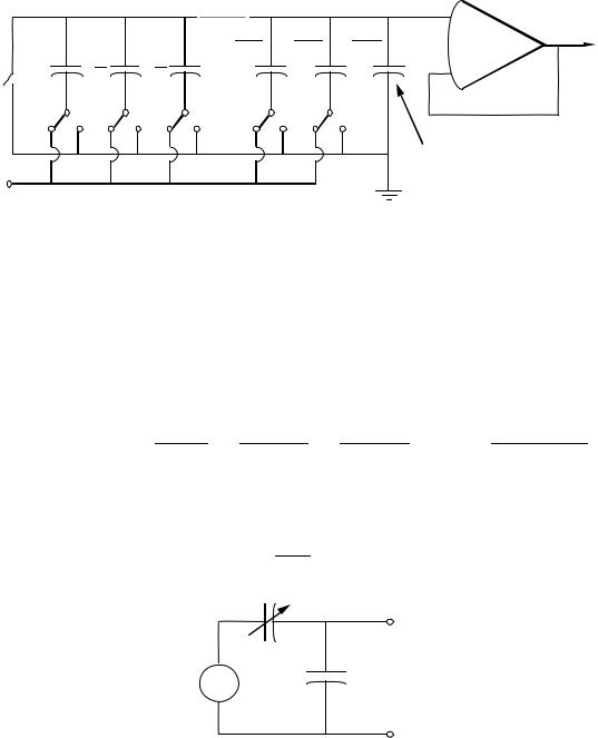
X.3 CHARGE SCALING D/A CONVERTER
Binary weighted capacitor array:
|
|
|
|
|
|
C |
|
C |
|
C |
|
|
|
|
vOUT |
||
|
C |
C |
C |
|
|
2N-2 |
|
2N-1 |
|
2N-1 |
|
|
|
|
|
||
|
|
|
|
|
|
|
|
|
|
|
|
|
|
|
|||
φ |
2 |
4 |
|
|
|
|
|
|
|
|
|
|
|
|
|
|
|
|
|
|
|
|
|
|
|
|
|
|
|
|
|
|
|||
1 |
|
|
|
|
|
|
|
|
|
|
|
|
|
|
|
|
|
|
SN-1 |
SN-2 |
SN-3 |
|
|
S1 |
|
|
S0 |
|
|
|
|
|
|
|
|
|
φ |
φ |
φ |
|
|
|
|
φ |
|
φ |
|
|
|
|
|
|
|
|
2 |
2 |
2 |
|
|
|
|
2 |
|
|
2 |
|
Terminating |
|
|
|
|
|
|
|
|
|
|
|
|
|
|
|
|
|
capacitor |
|
|
|
|
VREF |
|
|
|
|
|
|
|
|
|
|
|
|
|
|
|
|
|
Operation: |
|
|
|
|
|
|
|
|
|
|
|
|
|
|
|
|
|
1.) |
During φ1, all capacitors are discharged. |
|
|
|
|
|
|||||||||||
2.) |
During φ2, |
capacitors |
with |
bi = |
1 are connected to VREF and |
||||||||||||
|
capacitors with bi = 0 are grounded. |
|
|
|
|
|
|
||||||||||
3.) The resulting output voltage is, |
|
|
|
|
|
|
|
|
|||||||||
|
|
|
|
|
|
bN-2C/2 |
bN-3C/4 |
b 0 C / |
( |
2 |
N-1) |
||||||
|
|
|
bN-1C |
|
|
|
|
||||||||||
|
vOUT = VREF 2C |
+ |
|
|
2C |
|
+ |
|
2C |
+ ... + |
2 C |
|
|||||
If Ceq. is defined as the sum of all capacitances connected to VREF, then |
|||||||||||||||||
|
|
|
|
v |
|
|
|
C |
|
V |
|
|
|
|
|
|
|
|
|
|
|
OUT |
= |
eq. |
REF |
|
|
|
|
|
|||||
|
|
|
|
|
|
2C |
|
|
|
|
|
|
|
||||
+Ceq.
VREF |
vOUT |
|
2C-Ceq. |
-

Allen and Holberg - CMOS Analog Circuit Design |
Page X.3-2 |
Other Versions of the Charge Scaling D/A Converter
Bipolar Operation:
Charge all capacitors to VREF. If bi = 1, connect the capacitor to ground, if bi = 0, connect the capacitor to VREF.
Will require an extra bit to decide whether to connect the capacitors initially to ground or to VREF.
Four-Quadrant Operation:
If VREF can have ±values, then a full, four quadrant DAC can be obtained.
Multiplying DAC:
If VREF is an analog signal (sampled and held), then the output is the product of a digital word and an analog signal and is called a multiplying DAC (MDAC).
Allen and Holberg - CMOS Analog Circuit Design |
Page X.3-4 |
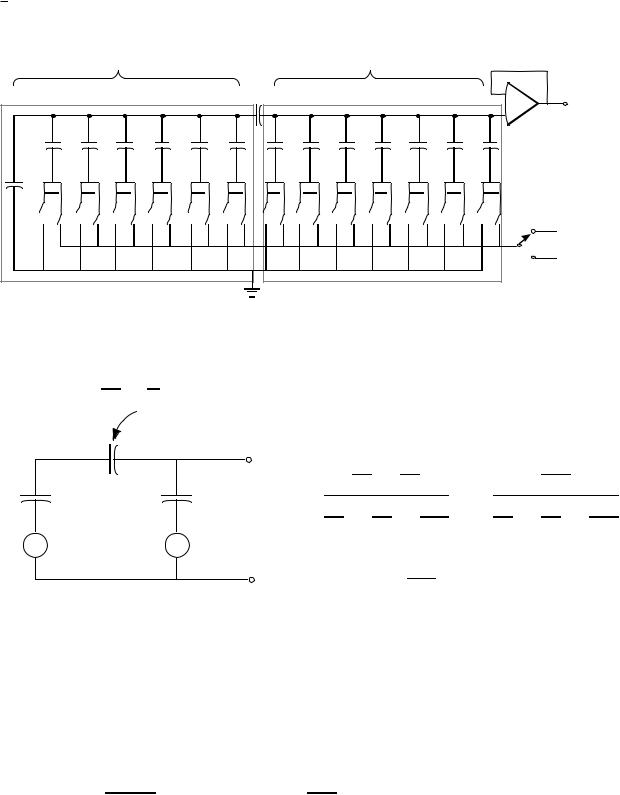
Increasing the Number of Bits for a Charge Scaling D/A Converter
Use a capacitive divider. For example, a 13-bit DAC-
|
|
|
LSB Array |
|
|
|
|
|
|
|
MSB Array |
|
|
|
|
|
|
|
|||||||
|
|
|
|
|
|
|
|
|
|
|
|
1.016pF (Attenuating capacitor) |
|
|
- |
|
|
|
|
||||||
|
|
|
|
|
|
|
|
|
|
|
|
|
|
|
|
|
|
|
|
|
+ |
|
vOUT |
|
|
|
|
|
|
|
|
|
|
|
|
|
|
|
|
|
|
|
|
|
|
|
|
|
|
|
|
|
|
1pF |
2pF |
|
4pF |
|
8pF |
16pF |
|
32pF |
1pF |
2pF |
4pF |
8pF |
16pF |
32pF |
64pF |
|
|
|
|||||
|
|
|
|
|
|
|
|
|
|
|
|
|
|
|
|
|
|
|
|
|
|
|
|
||
|
1pF |
|
|
|
|
|
|
|
|
|
|
|
|
|
|
|
|
|
|
|
|
|
|
|
|
|
|
b0 |
b1 |
|
b2 |
b3 |
|
b4 |
b5 |
b6 |
b7 |
b8 |
b9 |
|
b10 b11 b12 |
|
|
|
|
||||||
|
|
b0 |
b1 |
|
|
b2 |
|
b |
|
b4 |
|
b5 |
b6 |
b7 |
|
b8 |
|
b9 |
b10 |
b11 |
b12 +VREF |
|
|
||
|
|
|
|
|
|
|
|
|
3 |
|
|
|
|
|
|
|
|
|
|
|
|
|
|
|
|
|
|
|
|
|
|
|
|
|
|
|
|
|
|
|
|
|
|
|
|
|
|
|
-VREF |
|
|
|
|
|
5 |
±biCi VREF |
|
|
|
|
|
|
|
12 |
±bi Ci VREF |
|
|
|
|
|
|
||||||
|
|
VL =∑ |
|
|
64 |
|
|
|
|
|
|
VR = ∑ |
|
127 |
|
|
|
|
|
|
|||||
|
|
|
i=0 |
|
|
|
|
|
|
|
|
|
|
i=6 |
|
|
|
|
|
|
|
||||
|
|
|
|
|
|
|
|
|
|
|
|
|
|
|
|
|
|
|
|
|
|
|
|
||
An equivalent circuit- |
|
|
|
|
|
|
|
|
|
|
|
|
|
|
|
|
|
||||||||
|
|
|
1 |
|
|
+ |
1 |
= 1 C = |
64 ≈ 1.016 |
|
|
|
|
|
|
|
|
|
|||||||
|
|
|
64 |
|
|
C |
|
|
|
|
|
63 |
|
|
|
|
|
|
|
|
|
|
|
|
|
|
|
|
|
|
|
|
|
|
|
|
|
+ |
|
|
|
1 |
+ |
6 3 |
|
|
|
1 |
|
|
|
|
|
64pF |
1.016pF |
|
|
|
127pF |
|
vOUT = 1 |
64 |
64 |
VR + |
|
|
127 |
|
1 VL |
||||||||
|
|
|
|
|
|
|
|
|
|
6 3 |
|
1 |
1 |
|
6 3 |
|
|||||||||
|
+ |
|
|
|
|
|
|
+ |
|
|
|
|
|
64 |
+ |
64 |
+ |
127 |
|
64 |
+ |
64 |
+ |
127 |
|
VL |
|
|
|
|
VR |
|
|
|
|
|
|
|
|
|
|
|
|
|
|
|
|
|
|||
|
- |
|
|
|
|
|
|
- |
|
|
|
- |
|
127 |
|
|
1 |
|
|
|
|
|
|
||
|
|
|
|
|
|
|
|
|
|
|
|
|
= 128 VR + 128 VL |
|
|
|
|
|
|||||||
|
|
|
|
|
|
|
|
|
|
|
|
|
|
|
|
|
|
|
|||||||
|
|
12 |
|
|
|
|
|
|
|
|
|
|
5 |
|
|
|
|
|
|
|
|
|
|
|
|
V |
R |
= ∑±biVREFCi |
|
and V |
L |
= ∑±biVREFCi |
|
|
|
|
|
|
|
|
|||||||||||
|
|
127 |
|
|
|
|
|
|
64 |
|
|
|
|
|
|
|
|
|
|
||||||
|
|
i=6 |
|
|
|
|
|
|
|
|
|
i=0 |
|
|
|
|
|
|
|
|
|
|
|
|
|
or |
|
|
|
|
|
|
12 |
|
|
|
|
|
|
|
|
|
|
|
|
|
|
|
|||
|
|
|
|
|
|
|
|
|
|
5 |
|
|
|
|
|
|
|
|
|
|
|
||||
|
|
|
±V |
REF |
|
|
|
|
|
|
b C |
|
|
|
|
|
|
|
|
|
|
||||
|
|
|
|
|
|
∑biCi + ∑ |
i |
i |
|
|
|
|
|
|
|
|
|
|
|||||||
|
|
vOUT = |
128 |
|
64 |
|
|
|
|
|
|
|
|
|
|
|
|||||||||
|
|
|
|
|
|
|
|
i=6 |
|
|
i=0 |
|
|
|
|
|
|
|
|
|
|
|
|
||
Allen and Holberg - CMOS Analog Circuit Design |
Page X.3-5 |
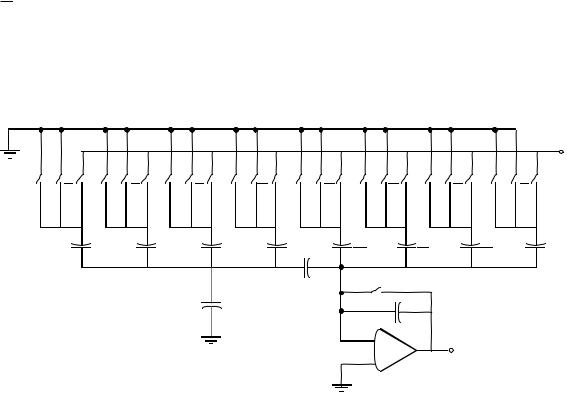
Removal of the Amplifier Input Capacitance Effects
Use the binary weighted capacitors as the input to a charge amplifier. Example of A Two-Stage Configuration:
VREF
φ1 b0 b0 φ1 b1 b1 |
φ1 b2 b2 |
φ1 b3 b3 φ1 b4 b4 |
φ1 b5 b5 |
φ1 b6 b6 |
φ1 b7 b7 |
|
||
C |
C |
C |
C |
C |
C |
C |
C |
|
8 |
4 |
2 |
8 |
4 |
2 |
|||
|
|
|||||||
|
|
|
C |
φ |
|
|
|
|
|
|
|
8 |
|
|
|
||
|
|
|
|
1 |
|
|
|
|
|
|
|
|
|
2C |
|
|
|
|
|
|
|
- |
vOUT |
|
||
|
|
|
|
+ |
|
|||
|
|
|
|
|
|
|
||
Allen and Holberg - CMOS Analog Circuit Design |
Page X.4-1 |
X.4 - VOLTAGE SCALING-CHARGE SCALING DAC'S
VREF
 R(2M-1)
|
|
|
SF |
|
vOUT |
R(2M-2) |
|
|
|
|
|
|
|
|
|
|
|
|
Ck-1 |
Ck-2 |
C1 |
C0 |
|
R(2M-3) |
2k-1 C |
2k-2 C |
2C |
C |
C |
|
|
|
|
||
M = 4 |
|
|
k = 8 |
|
|
|
SA |
|
|
A |
|
R1 |
S |
S |
S |
S |
|
|
1A |
0A |
|
||
|
(k-1)A |
(k-2)A |
|
|
|
|
S(k-1)B |
S(k-2)B |
S |
S |
|
|
SB |
|
1B |
0B |
|
|
|
|
B |
|
|
R0 |
|
|
|
|
Advantages:
•Resistor string is inherently monotonic so the first M bits are monotonic.
•Can remove voltage threshold offsets.
•Switching both busses A and B removes switch imperfections.
•Can make tradeoffs in performance between the resistors and capacitors.
•Example with 4 MSB's voltage scaling and 8 LSB's charge scaling:
Allen and Holberg - CMOS Analog Circuit Design |
Page X.4-2 |
Voltage Scaling, Charge Scaling DAC - Cont'd
Operation:
1.) SF, SB, and S1B through Sk,B are closed discharging all capacitors. If the output of the DAC is applied to any circuit having a nonzero threshold, switch SB could be connected to this circuit to cancel this threshold effect.
2.) Switch SF is opened and buses A and B are connected across the resistor whose lower and upper voltage is V'REF and V'REF respectively, where
|
' |
|
|
b0 |
b1 |
b2 |
|
b M - 1 |
|
V |
|
= Vref |
|
+ 2M-1 |
+ 2M-2 |
+ ···· + |
21 |
|
|
REF |
2M |
|
|||||||
|
|
|
|
|
|
|
|
|
+ |
|
|
|
2k-1 C |
|
2k-2 C |
|
2C |
C |
C |
|
|
A |
|
|
|
|
|
vOUT |
|
+ |
|
|
|
S2A |
SA |
|
|||
|
Sk,A |
Sk-1,A |
|
|
|||||
2-MV REF
- |
B |
Sk,B |
Sk-1,B |
S2B |
SB |
- |
|
|
|
|
|
|
+
V 'REF
-
3.) Final step is to determine whether to connect the bottom plates of the capacitors to bus A (bi=1) or bus B (bi=0).
|
|
|
Ceq. |
|
|
|
M+K-1 |
|
|
|
|
|
+ |
|
|
|
|
|
|
|
|
|
|
∑bi2-(M+K-i) V |
|
|
2 |
-M |
VREF |
2KC - Ceq. |
v |
OUT |
= |
REF |
|
|
vOUT |
|
i=0 |
|||||
|
|
|
- |
|
|
|
|
-
+
V 'REF
-

Allen and Holberg - CMOS Analog Circuit Design |
Page X.4-3 |
Charge Scaling, Voltage Scaling DAC
Use capacitors for MSB's and resistors for LSB's
|
|
|
|
vOUT |
2N-1C 2N-2C |
2N-3C |
|
VREF |
C |
|
4C |
2C |
C |
|
|
|
|
R |
|
VREF |
Switch network |
R |
|
|
|
|
MSBs |
R |
|
LSBs |
|
|
|
 R
R
 R
R
•Resistors must be trimmed for absolute accuracy.
•LSB's are monotonic.
Allen and Holberg - CMOS Analog Circuit Design |
Page X.5-1 |
X.5- OTHER TYPES OF D/A CONVERTERS
CHARGE REDISTRIBUTION SERIAL DAC
S2 |
Precharge to |
|
|
Initially |
|
|
VREF if bi = "1" |
Redistribution |
|
||||
VREF |
discharge S4 C1 = C2 |
|||||
|
|
switch |
||||
S3 |
S1 |
|
S4 |
b0 = LSB |
||
|
b1 |
= NLSB |
||||
|
|
|
|
|||
|
+ |
|
+ |
. |
|
|
|
|
. |
|
|||
C1 |
VC1 |
C2 |
VC2 |
|
||
. |
|
|||||
Precharge C1 |
- |
|
- |
|
||
to ground if |
|
bN |
= MSB |
|||
|
|
|
||||
bi = "0"
Conversion sequence:
4 Bit D/A Converter
INPUT WORD: 1101 |
|
|
|
|
|
|
|
|
|
|
|
|
|
||||
1 |
|
|
|
|
Close |
S4: VC2 = |
0 |
|
|
|
|
|
|
|
|||
3/4 |
|
|
|
13/16 |
Start with LSB first- |
|
|
|
|
|
|
||||||
VC1/VREF 1/2 |
|
|
|
|
Close |
S2 |
(b0=1): |
VC1 |
= VREF |
||||||||
|
|
|
|
|
|
|
|
|
VREF |
|
|
|
|
|
|||
1/4 |
|
|
|
|
Close |
S1: VC1 = |
|
= VC2 |
|||||||||
|
|
|
|
|
2 |
|
|
||||||||||
0 |
2 |
4 |
6 |
8 |
Close |
S3 |
(b1=0): |
VC1 |
= 0 |
|
|
|
|||||
|
|
|
|
|
|
|
|
|
VREF |
|
|||||||
|
|
|
|
|
Close |
S1: VC1 = VC2 = |
|
||||||||||
1 |
|
|
|
|
4 |
|
|
||||||||||
|
|
|
|
Close |
S2 |
(b2=1): |
VC1 |
= VREF |
|||||||||
3/4 |
|
|
|
13/16 |
|||||||||||||
|
|
|
|
|
|
|
|
|
|
|
|
|
5 |
|
|
|
|
VC2/VREF 1/2 |
|
|
|
|
Close |
S : V |
C1 |
= V |
C2 |
= |
V |
REF |
|||||
|
|
|
|
|
1 |
|
|
|
|
|
8 |
|
|||||
1/4 |
|
|
|
|
Close |
S2 |
(b3=1): |
VC1 |
= VREF |
||||||||
|
|
|
|
|
Close |
S : V |
C1 |
= V |
C2 |
= |
13 V |
REF |
|||||
0 |
2 |
4 |
6 |
8 |
|
1 |
|
|
|
|
|
16 |
|
|
|||
|
|
|
|
|
|
|
|
|
|
|
|
||||||
Comments:
•LSB must go first.
•n cycles to make an n-bit D-A conversion.
•Top plate parasitics add error.
•Switch parasitics add error.