

Allen and Holberg - CMOS Analog Circuit Design
Design Procedure:
This design procedure assumes that the gain at dc (Av), unity gain bandwidth (GB), input common mode range (Vin(min) and Vin(max)), load capacitance (CL), slew rate (SR), settling time (Ts), output voltage swing (Vout(max) and Vout(min)), and power dissipation (Pdiss) are given.
1.Choose the smallest device length which will keep the channel modulation parameter constant and give good matching for current mirrors.
2.From the desired phase margin, choose the minimum value for Cc, i.e. for a 60° phase margin we use the following relationship. This assumes that z ≥ 10GB.
Cc > 0.22CL
3.Determine the minimum value for the “tail current” (I5) from the largest of the two values.
I5 = SR .Cc |
|
|
|
||
|
V |
+ |V |
| |
||
I5 |
10 |
DD |
SS |
|
|
|
|
2 .Ts |
|
|
|
4.Design for S3 from the maximum input voltage specification.
S3 = |
I5 |
≥ 1 |
|
K'3[VDD − Vin(max) − |VT03|(max) + VT1(min)]2 |
|||
|
|
5.Verify that the pole of M3 due to Cgs3 and Cgs4 (=0.67W3L3Cox) will not be dominant by assuming it to be greater than 10 GB
gm3 > 10GB. 2Cgs3
6.Design for S1 (S2) to achieve the desired GB.
gm1 = GB . Cc S2 = g2m2 K'2I5
7.Design for S5 from the minimum input voltage. First calculate VDS5(sat) then find S5.
VDS5(sat) = Vin(min) − VSS − |
I5 |
− VT1(max) ≥ 100 mV |
||
β1 |
||||
|
|
|
||
S5 = K' [V |
2I5 |
|
|
|
(sat)]2 |
|
|
||
5 |
DS5 |
|
|
|

Allen and Holberg - CMOS Analog Circuit Design
8.Find gm6 and S6 by the relationship relating to phase margin, load, and compensation capacitors, and the balance condition.
gm6 = 2.2gm2(CL/Cc)
S |
|
gm6 |
|
|
= S |
|
|
|
6 |
3 gm3 |
|
9. Calculate I6 :
I6 = (S6/S4)I4 = (S6/S4)(I5/2)
10. Design S7 to achieve the desired current ratios between I5 and I6.
S7 = (I6/I5)S5
11. Check gain and power dissipation specifications.
Av = |
2gm2gm6 |
|
+ λ3)I6(λ6 + λ7) |
||
I5(λ2 |
Pdiss = (I5 + I6)(VDD + |VSS|)
12.If the gain specification is not met, then the currents, I5 and I6, can be decreased or the W/L ratios of M2 and/or M6 increased. The previous calculations must be rechecked to insure that they have been satisfied. If the power dissipation is too high, then one can only reduce the currents I5 and I6. Reduction of currents will probably necessitate increase of some of the W/L ratios in order to satisfy input and output swings.
13.Simulate the circuit to check to see that all specifications are met.

Allen and Holberg - CMOS Analog Circuit Design
Example: Design of a Two-Stage Op Amp
Using the material and device parameters given in Tables 3.1-1 and 3.1-2, design an amplifier similar to that shown in Fig. 6.3-1 that meets the following specifications. Assume the channel length is to be 1µm.
Av > 3000V/V |
VDD = 2.5V |
VSS = -2.5V |
GB = 5MHz |
CL = 10pF |
SR > 10V/µs |
Vout range = ±2V |
ICMR = -1 to 2V |
Pdiss ≤ 2mW |
Solution
Calculate the minimum value of the compensation capacitor Cc,
Cc > (2.2/10)(10 pF) = 2.2 pF
Choose Cc as 3pF. Using the slew-rate specification and Cc calculate I5.
I5 = (3 × 10-12)(10 × 106) = 30 µA
Next calculate (W/L)3 using ICMR requirements.
30 × 10-6
(W/L)3 = (50 × 10-6)[2.5 − 2 − .85 + 0.55]2 = 15
gm3 =  2 × 50x10-6 x15x10-6 × 15 = 150µS
Therefore
(W/L)3 = (W/L)4 = 15
Check the value of the mirror pole, p3, to make sure that it is in fact greater than 10GB. Assume the Cox = 0.4fF/µm2. The mirror pole can be found as
p3 ≈ |
-gm3 = |
- 2K’pS3I3 |
= 15.75x10⁹(rads/sec) |
|
2Cgs3 |
2(0.667)W3L3Cox |
|
or 2.98 GHz. Thus, p3, is not of concern in this design because p3 >> 10GB.
The next step in the design is to calculate gm1
gm1 = (5 × 10⁶)(2π)(3 × 10-12) = 94.25µS
Therefore, (W/L)1 is
|
2 |
|
|
|
(W/L)1 = (W/L)2 = |
gm1 |
= |
(94.25)2 |
= 2.79 ≈ 3.0 |
|
2K’NI1 |
|
2·110·15 |
|
Next calculate VDS5
Allen and Holberg - CMOS Analog Circuit Design
VDS5 |
= (−1) − (−2.5) − |
30 × 10-6 |
|
110 |
- .85 = 0.35V |
||
|
|
× 10-6·3 |
|
Using VDS5 calculate (W/L)5 from Eq. (16)
2(30 × 10-6)
(W/L)5 = (50 × 10-6)(0.35)2 = 4.49 ≈ 4.5
From Eq. (20) of Sec. 6.2, we know that gm6 ≥ 10gm1 ≥ 942.5µS
Assuming that gm6 = 942.5µS
(W/L)6 |
= 15 |
942.5 × 10⁻⁶ |
|
150 |
= 94.25 |
||
|
|
× 10-6 |
|
Using the equations for proper mirroring, I6 is determined to be
I6 = (15 × 10-6)(94.25/15) = 94.25 µA
Finally, calculate (W/L)7 |
|
|
|
(W/L)7 |
94.25 × 10⁻⁶ |
≈ 14.14 |
|
= 4.5 |
|
||
|
30 × 10-6 |
|
|
Check the Vout(min) specification although the W/L of M7 is so large that this is probably not necessary. The value of Vout(min) is
2 × 94.25 |
|
Vmin(out) = VDS7(sat) = |
= 0.348V |
110 |
× 14.14 |
which is much less than required. At this point, the first-cut design is complete. Examining the results shows that the large value of M7 is due to the large value of M5 which in turn is due to a tight specification on the negative input common mode range. To reduce these values the specification should be loosened or a different architecture (i.e. p-channel input pair) examined.
Now check to see that the gain specification has been met
(2)(94.25 × 10⁻⁶)(942.5 × 10⁻⁶)
Av = 30 × 10-6(.04 + .05)38 × 10-6(.04 + .05) = 19,240 which meets specifications.
Allen and Holberg - CMOS Analog Circuit Design
IX. HIGH PERFORMANCE CMOS AMPLIFIERS
Contents
IX.1 |
Improving The Two-Stage Architecture |
IX.2 |
Two-stage Cascode Architecture |
IX.3 |
Folded Cascode Architecture |
IX.4 |
Differential Output Architecture (Class AB) |
IX.5 |
Low power amplifiers |
IX.6 |
Dynamically biased amplifiers |
IX.7 |
|
Organization |
|
|
|
|
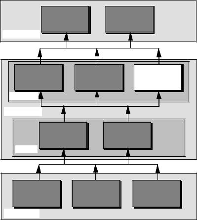
Chapter 10 |
Chapter 11 |
|||
D/A and A/D |
||||
Analog Systems |
||||
Converters |
||||
|
|
|||
SYSTEMS |
|
|
|
|
Chapter 7 |
|
Chapter 8 |
Chapter 9 |
|
CMOS |
Simple CMOS Op |
High Performance |
||
Comparators |
|
Amps |
OTA's |
|
COMPLEX |
|
|
|
|
CIRCUITS |
|
|
|
|
Chapter 5 |
|
Chapter 6 |
||
CMOS |
|
CMOS Amplifiers |
||
Subcircuits |
|
|
||
SIMPLE |
|
|
|
|
Chapter 2 |
|
Chapter 3 |
Chapter 4 Device |
|
CMOS |
CMOS Device |
|||
Characterization |
||||
Technology |
|
Modeling |
||
|
|
|||
DEVICES |
|
|
|
|
Allen and Holberg - CMOS Analog Circuit Design
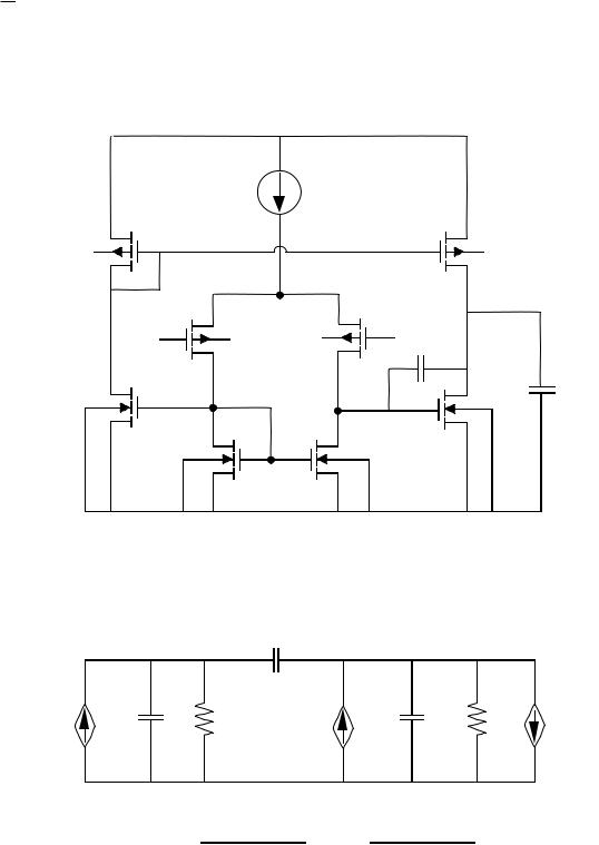
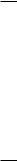
IX.1 IMPROVING THE TWO-STAGE ARCHITECTURE
Amplifiers Using an MOS Output Stage
PUSH-PULL CMOS OTA
This amplifier is a simple extension of the seven-transistor OTA
studied in Section 8.
VDD
V |
M9 |
|
M7 |
VDD |
|
|
|
||
DD |
|
|
|
|
|
|
|
|
vOUT |
|
M1 |
M2 |
|
|
|
- |
VDD |
+ |
|
|
|
|
Cc |
|
|
M8 |
|
|
CL |
|
|
|
M6 |
|
|
M3 |
M4 |
|
|
small-signal equivalent circuit:
|
|
|
Cc |
|
|
vout |
|
|
|
|
|
|
|
|
|
+ |
|
|
|
|
gm1vi |
C1 |
r1 v1 |
gm6v1 |
CL |
r2 |
gm1Ai vi |
|
|
|
|
|
|
2 |
-
where gm1 |
= gm2, r1 |
= |
|
1 |
, r2 |
= |
|
1 |
|
gds2 |
+ gds4 |
gds6 |
+ gds7 |
||||||
|
|
|
|
|

Allen and Holberg - CMOS Analog Circuit Design
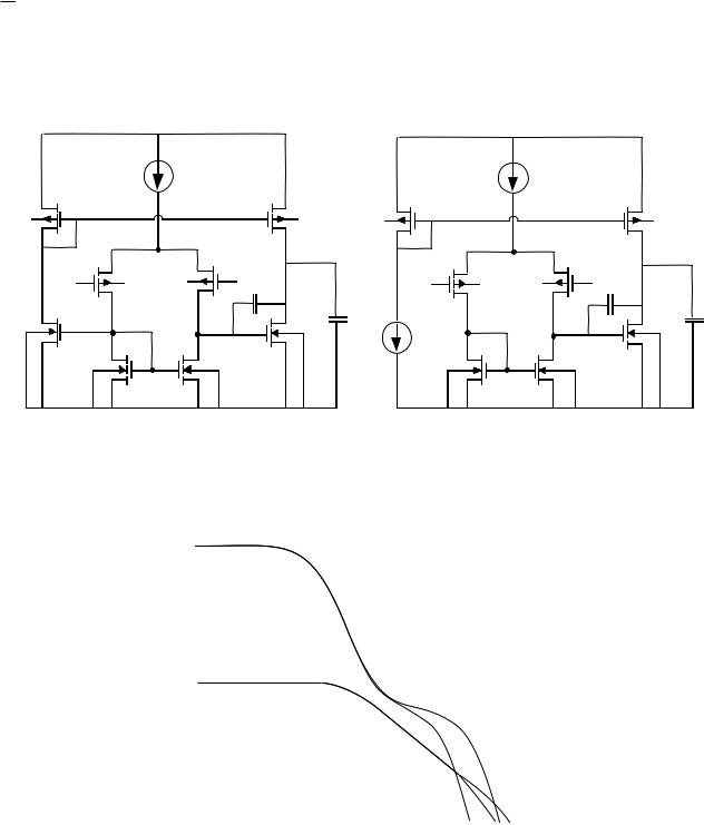
Amplifiers Using an MOS Output Stage - Continued
Network equations:
[g1 + s(C1 + CL)]v1 - sCcv2 = gm1vi
|
|
gm1AIvi |
|||
[g5 + sCc]v1 + [g2 + s(Cc + CL)]v2 = 2 |
|
i7 |
|||
AI is the current gain from M1 to M7: AI |
= |
||||
i1 |
|||||
|
-gm6 |
|
|||
|
|
|
|||
z = A |
|
|
|
||
|
I |
- 1 C |
|
|
|
|
2 |
c |
|
|
|
p1 |
≈ |
-g1g2 |
|
gm6Cc |
|||
|
|
||
p2 |
≈ |
-gm6 |
|
CL |
|||
|
|
≈ gm1gm6
AV g1g2
To guarantee that the zero stays in the left-half plane, AI > 2
Allen and Holberg - CMOS Analog Circuit Design
Amplifiers Using an MOS Output Stage - Continued
Example:
VDD |
VDD |
|
M9 |
M7 |
VDD |
M9 |
M7 |
VDD |
VDD |
|
VDD |
|
- |
VDD |
+ |
- |
M1 |
M2 |
+ |
|
|
M1 |
M2 |
|
|
|
||
|
|
|
Cc |
|
|
|
Cc |
M8 |
|
|
CL |
|
|
|
CL |
|
|
|
|
|
|
|
|
|
|
|
M6 |
|
|
|
M6 |
|
M3 |
M4 |
|
|
M3 |
M4 |
|
|
Push-Pull (AI ≈ 3) |
Standard (AI = 0) |
|
||||
140 |
|
|
|
|
|
|
|
|
|
|
|
|
|
|
|
|
|
|
|
|
|
|
|
|
|
|
|
|
|
|
|
|
|
|
|
|
|
120 |
|
|
|
|
|
|
|
|
|
|
|
|
|
|
|
|
|
|
|
|
|
|
|
|
|
|
|
|
|
|
|
|
|
|
|
|
|
100 |
|
|
|
|
|
|
|
|
|
|
|
|
|
|
|
|
|
|
|
|
|
|
|
|
|
|
|
|
|
|
|
|
|
|
|
|
|
80 |
|
|
|
|
|
|
|
|
|
|
|
|
|
|
|
|
|
|
|
|
|
|
|
|
|
|
|
|
|
|
|
|
|
|
|
|
|
Gain(db) |
|
|
|
|
|
|
|
|
|
Push-Pull phase |
|
|
||||||
60 |
|
|
|
|
|
|
|
|
|
|
|
|
||||||
|
|
|
|
|
|
|
|
|
|
|
|
Standard gain |
|
|||||
40 |
|
|
|
|
|
|
|
|
|
|
|
|
|
|||||
|
|
|
|
|
|
|
|
|
|
|
|
|
|
Push-Pull |
|
|||
|
|
|
|
|
|
|
|
|
|
|
|
|
|
|
||||
20 |
|
|
|
|
|
|
|
|
|
|
|
|
|
|
|
|||
|
|
|
|
Standard phase |
|
|
|
|
gain |
|
|
|||||||
|
|
|
|
|
|
|
|
|
|
|
||||||||
0 |
|
|
|
|
|
|
|
|
|
|
|
|
||||||
|
|
|
|
|
|
|
|
|
|
|
|
|
|
|
|
|
|
|
|
|
|
|
|
|
|
|
|
|
|
|
|
|
|
|
|
|
|
-20 |
|
|
|
|
|
|
|
|
|
|
|
|
|
|
|
|
|
|
|
|
|
|
|
|
|
|
|
|
|
|
|
|
|
|
|
|
|
|
|
|
|
|
|
|
|
|
|
|
|
|
|
|
|
|
|
|
101 |
102 |
103 |
104 |
105 |
106 |
107 |
108 |
109 |
||||||||||
|
|
|
|
|
|
|
|
|
Frequency |
|
|
|
|
|
|
|||
Allen and Holberg - CMOS Analog Circuit Design
IX.2 Two-Stage Cascode Architecture
Why Cascode Op Amps?
•Control the frequency behavior
•Increase PSRR
•Simplifies design
Where is the Cascode Technique Applied?
• First stage -
Good noise performance
Requires level translation to second stage
Requires Miller compensation
• Second stage -
Self compensating
Reduces the efficiency of the Miller compensation Increases PSRR
Allen and Holberg - CMOS Analog Circuit Design
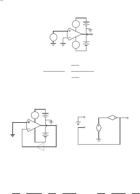
Power Supply Rejection Ratio (PSRR)
Definition:
|
|
+ |
+ |
|
|
vdd |
VDD |
|
+ |
- |
- |
|
|
vout |
|
vin |
|
|
|
- |
+ |
+ |
|
|
vss |
VSS |
|
|
|
- |
|
|
|
- |
|
|
|
|
vout
Av(vdd=0) vin (vdd=0)
PSRR+ = Add(vin=0) = vout
vdd (vin=0)
Calculation of PSRR:
|
+ |
+ |
|
|
|
|
Addvdd |
|
||
|
vdd |
|
|
VDD |
|
|
v1 |
vout |
||
|
- |
|
|
|
|
|||||
|
- |
|
|
|
|
|
||||
|
|
|
|
|
|
|
|
|||
|
|
|
|
|
|
|
|
|
|
|
|
|
|
|
|
vout |
v2 |
Av(v1 -v2) |
|
||
|
|
+ |
|
|
=> |
|
||||
|
|
VSS |
|
|
|
|
|
|||
|
|
- |
|
|
|
|
|
|
||
|
|
|
|
|
|
|
|
|
||
|
|
|
|
|
|
|
|
|
|
|
|
|
K |
|
|
|
|
|
|
|
|
vout = Addvdd + Av(v1-v2) = Addvdd - Avvout |
|
|
||||||||
vout(1 + Av) = Addvdd |
|
|
|
Extends bandwidth beyond GB |
||||||
vout = |
|
|
|
|
|
|
|
|
↓ |
|
Add |
|
≈ |
Add |
= |
1 |
|
vout = |
KAdd |
≈ Add |
|
vdd |
1 + Av |
Av |
|
PSRR+ |
|
vdd |
1+KAv |
Av |
||