

Allen and Holberg - CMOS Analog Circuit Design |
Page IV.5-4 |
CGB0
Drain
Gate overhang
Gate
Source
FOX |
FOX |
|
Diffusion source |
CGB |
Cpoly-field |
Figure B.6-4 Illustration of gate-to-bulk and poly-field capacitance.
This capacitance is approximated from the interconnect capacitance Cpoly-field (overhang capacitor is not a true parallel-plate capacitor)
Cpoly-field = |
Cmeas |
(2) |
(F/m2) |
||
|
LRWR |
|
where
Cmeas = Cmeas = measured value of the polysilicon strip
LR = length of the centerline of the polysilicon strip
WR = width of the polysilicon strip (usually chosen as device length)
Having determined Cpoly-field, CGB0 can be approximated as |
|
CGB0 2 (Cpoly-field)(doverhang) = 2C5 (F/m) |
(3) |
where |
|
doverhang = overhang dimension (see Rule 3D, Table 2.6-1) |
|
4
Allen and Holberg - CMOS Analog Circuit Design |
|
|
|
Page IV.5-5 |
||||
CBD and CBS |
|
|
|
|
|
|
|
|
|
|
V |
-MJ |
|
|
V |
-MJSW |
|
|
+ |
|
J |
|
+ |
|
J |
(4) |
CJ(VJ) = ACJ(0) 1 |
PB |
+ PCJSW(0) 1 |
PB |
|||||
where
VJ = the reverse bias voltage across the junction
CJ(VJ) = bottom junction capacitance at VJ
CJSW(VJ) = junction capacitance of sidewall at VJ
A = area of the (bottom) of the capacitor
P = perimeter of the capacitor
PB = bulk junction potential
The constants CJ and MJ can be determined by measuring a large
rectangular capacitor structure where the contribution from the sidewall capacitance is minimal. For such a structure, CJ(VJ) can be approximated
as
|
|
V |
J |
-MJ |
|
||
|
+ |
|
|
|
|
|
|
CJ(VJ) = ACJ(0) 1 |
PB |
|
|
|
|||
This equation can be rewritten in a |
way that is convenient for |
||||||
regression. |
|
|
|
|
|
|
|
|
|
|
|
|
V |
|
|
|
|
|
|
+ |
|
J |
+ log[ACJ(0)] |
log[CJ(VJ)] = (−MJ)log 1 |
PB |
||||||
(5) linear
(6)
Plotting log[CJ(VJ)] versus log[1 + VJ/PB] and determine the slope, −MJ, and the Y intercept (where Y is the term on the left), Log[ACJ(0)]. Knowing the area of the capacitor, the calculation of the bottom junction capacitance is straightforward.
5
Allen and Holberg - CMOS Analog Circuit Design |
Page V.0-1 |
V. CMOS SUBCIRCUITS
Contents
V.1 MOS Switch
V.2 MOS Diode
V.3 MOS Current Source/Sinks
V.4 Current Mirrors/Amplifiers
V.5 Reference Circuits
V.5-1 Power Supply Dependence
V.5-2 Temperature Dependence
V.6 Summary
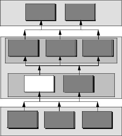
Organization
Chapter 10
Chapter 11
D/A and A/D
Analog Systems
Converters |
|
|
SYSTEMS |
|
|
Chapter 7 |
Chapter 8 |
Chapter 9 |
CMOS |
Simple CMOS |
High Performance |
Comparators |
Opamps |
Opamps |
COMPLEX |
|
|
CIRCUITS |
|
|
Chapter 5 |
Chapter 6 |
|
CMOS |
|
CMOS |
Subcircuits |
Amplifiers |
|
SIMPLE |
|
|
Chapter 2 |
Chapter 3 |
Chapter 4 |
CMOS |
CMOS Device |
Device |
Technology |
Modeling |
Characterization |
DEVICES |
|
|
Allen and Holberg - CMOS Analog Circuit Design |
Page V.0-2 |
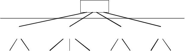
WHAT IS A SUBCIRCUIT?
A subcircuit is a circuit which consists of one or more transistors and generally perfoms only one function.
A subcircuit is generally not used by itself but in conjunction with other subcircuits.
Example
Design hierarchy of analog circuits illustrated by an op amp.
Operational
Amplifier
Complex Circuits |
|
|
|
|
|
|
|
|
|
|
|
|
|
|
|
|
|
|
|
|
|
|
||||
Simple Circuits |
|
|
|
|
|
|
|
|
|
|
|
|
|
|
|
|
|
|
|
|
|
|
||||
|
|
|
|
|
|
|
|
|
|
|
|
|
|
|
|
|
|
|
|
|
|
|
|
|
|
|
|
Biasing |
|
|
|
Input Different- |
|
|
|
|
Second Gain |
|
|
|
Output |
|
|||||||||||
|
Circuits |
|
|
|
|
ial Amplifier |
|
|
|
|
Stage |
|
|
|
Stage |
|
||||||||||
|
|
|
|
|
|
|
|
|
|
|
|
|
|
|
|
|
|
|
|
|
|
|
|
|
|
|
|
|
|
|
|
|
|
|
|
|
|
|
|
|
|
|
|
|
|
|
|
|
|
|
|
||
Current |
|
Current |
|
Current |
|
|
Diff. |
|
|
Mirror |
|
Inverter |
Current |
|
Source |
Current |
||||||||||
|
|
|
|
|
|
|
|
Sink |
|
|
Sink |
|||||||||||||||
Source |
|
Mirror |
|
Sink |
|
|
Amp. |
|
|
|
Load |
|
|
|
Follower |
|
||||||||||
|
|
|
|
|
|
|
|
|
|
|
Load |
|
|
Load |
||||||||||||
|
|
|
|
|
|
|
|
|
|
|
|
|
|
|
|
|
|
|
|
|
|
|
||||
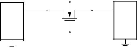
Allen and Holberg - CMOS Analog Circuit Design |
Page V.1-1 |
V.1 - MOS SWITCH
SWITCH PROPERTIES
Ideal Switch
RAB(on) = 0Ω
A
 B
B
RAB(off) = ∞
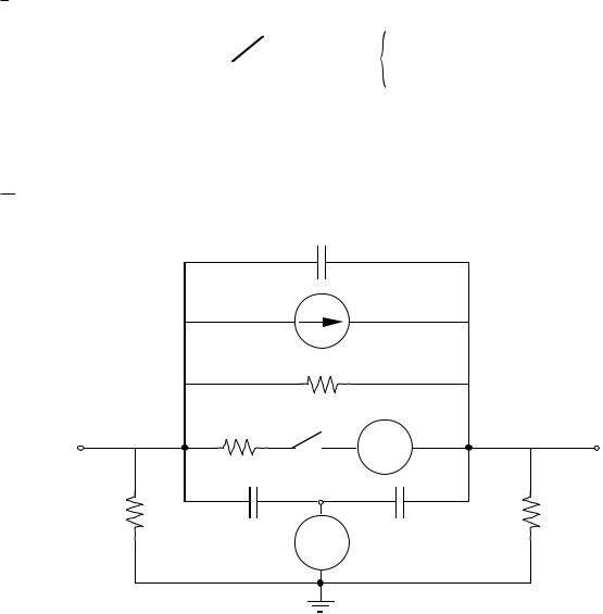
Nonideal Switch
|
CAB |
|
|
IOFF |
|
|
ROFF |
|
RON |
|
VOFF |
+ |
- |
|
A |
|
B |
CAC
C
RA |
+ |
CBC
RB
VControl
-

Allen and Holberg - CMOS Analog Circuit Design |
Page V.1-2 |
MOS TRANSISTOR AS A SWITCH
Symbol
|
|
|
Bulk |
A |
B |
A |
B |
|
|
||
|
|
(S/D) |
(D/S) |
C (G)
On Characteristics of A MOS Switch
Assume operation in non-saturation region (vDS < vGS - VT).
i |
|
K’W |
|
|
|
|
- V |
|
) - |
vD S |
|
|
||||||
D |
= |
|
|
(v |
G S |
T |
|
v |
DS |
|||||||||
|
|
|
L |
|
|
|
|
|
2 |
|
||||||||
|
∂iD |
= |
K’W |
v |
|
|
− V |
|
− v |
|
|
|||||||
∂vDS |
L |
|
|
|
|
|||||||||||||
|
|
|
|
G S |
|
|
|
T |
|
D S |
||||||||
Thus, |
|
|
|
|
|
|
|
|
|
|
|
|
|
|
|
|
||
|
|
|
|
|
|
|
|
∂vDS |
|
|
|
|
|
|
1 |
|||
|
|
|
|
RON = ∂iD |
= K’W |
|
|
|
||||||||||
|
|
|
|
|
|
|
|
|
|
|
|
|
|
L |
(vG S − V T − vD S ) |
|||
OFF Characteristics of A MOS Switch
If vGS < VT, then iD = IOFF = 0 when vDS ≈ 0V.
If vDS > 0, then
ROFF ≈ |
1 |
= |
1 |
≈ ∞ |
|
iDSλ |
|
IOFFλ |
|
Allen and Holberg - CMOS Analog Circuit Design |
Page V.1-3 |
MOS SWITCH VOLTAGE RANGES
Assume the MOS switch connects to circuits and the analog signal can vary from 0 to 5V. What are the voltages required at the terminals of the MOS switch to make it work properly?
|
|
Bulk |
|
|
(0 to 5V) |
(0 to 5V) |
|
Circuit |
(S/D) |
(D/S) |
Circuit |
|
|
||
1 |
|
|
2 |
|
|
G |
|
•The bulk voltage must be less than or equal to zero to insure that the bulk-source and bulk-drain are reverse biased.
•The gate voltage must be greater than 5 + VT in order to turn the switch on.
Therefore,
VBulk ≤ 0V
VG ≥ 5 + VT
(Remember that the larger the value of VSB, the larger VT)
Allen and Holberg - CMOS Analog Circuit Design |
Page V.1-4 |
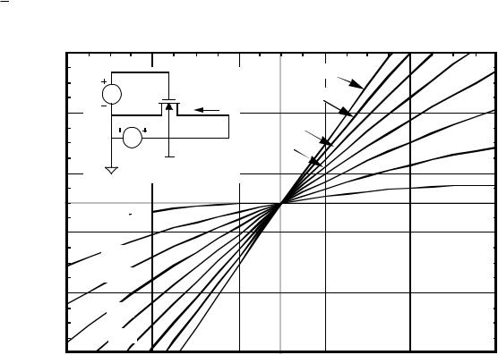
I-V CHARACTERISTICS OF THE MOS SWITCH
SPICE ON Characteristics of the MOS Switch
100 A 
|
V1 =10V |
|
V1 |
V1=9V |
|
60 A |
I d |
|
V1 =8V |
||
|
V1 =7V
V2
-5
20 A 
Id
V1=2V 
-20 A 
V1=3V
V1=4V
-60 A 
V1 =5V
V1 =6V
-100 A |
|
-0.2V |
0.2V |
0.6V |
1V |
-1V |
-0.6V |
||||
|
|
|
V2 |
|
|
SPICE Input File:
MOS Switch On Characteristics M1 1 2 0 3 MNMOS W=3U L=3U
.MODEL MNMOS NMOS VTO=0.75, KP=25U, +LAMBDA=0.01, GAMMA=0.8 PHI=0.6
V2 1 0 DC 0.0
V1 2 0 DC 0.0
V3 3 0 DC -5.0
.DC V2 -1 1 0.1 V1 2 10 1
.PRINT DC ID(M1)
.PROBE
.END
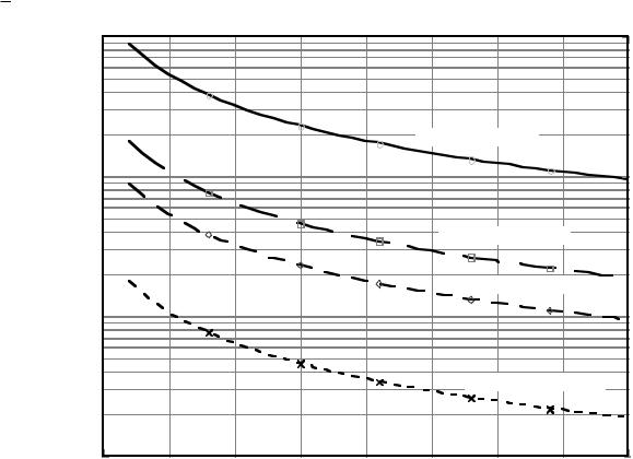
Allen and Holberg - CMOS Analog Circuit Design |
Page V.1-5 |
MOS SWITCH ON RESISTANCE AS A FUNCTION OF VG S
SPICE ON Resistance of the MOS Switch
100kΩ
ResistanceOnSwitch |
10kΩ |
|
|
MOS |
1kΩ |
|
W/L = 3µm/3µm
W/L = 15µm/3µm
W/L = 30µm/3µm
W/L = 150µm/3µm
100Ω |
|
|
|
|
|
|
|
|
1.0V |
1.5V |
2.0V |
2.5V |
3.0V |
3.5V |
4.0V |
4.5V |
5.0V |
Gate-Source Voltage
SPICE Input File:
MOS Switch On Resistance as a f(W/L) M1 1 2 0 0 MNMOS W=3U L=3U M2 1 2 0 0 MNMOS W=15U L=3U M3 1 2 0 0 MNMOS W=30U L=3U M4 1 2 0 0 MNMOS W=150U L=3U
.MODEL MNMOS NMOS VTO=0.75, KP=25U, LAMBDA=0.01, GAMMA=0.8 PHI=0.6
VDS 1 0 DC 0.001V VGS 2 0 DC 0.0
.DC VGS 1 5 0.1
.PRINT DC ID(M1) ID(M2) ID(M3) ID(M4)
.PROBE
.END
Allen and Holberg - CMOS Analog Circuit Design |
Page V.1-6 |
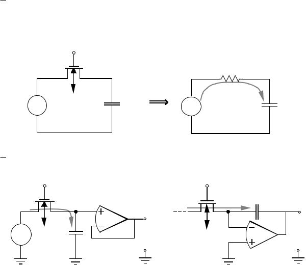
INFLUENCE OF SWITCH IMPERFECTIONS ON
PERFORMANCE
Finite ON Resistance
Non-zero charging and discharging rate.
φ1
|
|
|
|
|
|
RON |
|
+ |
VSS C1 |
+vC1 |
|
|
+ |
|
+ vC1 |
VIN |
|
|
V |
C1 |
|||
|
|
- |
|
|
IN |
|
- |
- |
|
|
|
- |
|
||
|
|
|
|
|
|
||
Finite OFF Current |
|
|
|
|
|
|
|
φ1 |
|
|
|
|
φ1 |
|
|
|
|
|
|
|
|
C2 |
|
+ |
|
|
+ |
|
|
+ |
|
|
|
|
|
|
|||
vIN VSS |
|
|
V |
|
vOUT |
||
C |
|
v |
|
|
|||
|
|
OUT |
SS |
|
|
||
|
Hold |
|
|
|
|
|
|
- |
|
|
|
- |
|
|
- |