

Allen and Holberg - CMOS Analog Circuit Design |
Page X.8-21 |
SELF-CALIBRATING ADC's
S1
MAINDAC
 COMP
COMP
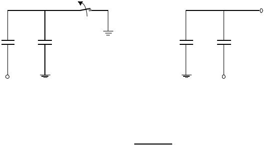
CN CN-1 C1B C1A CCAL
Vref
GND
CALIBRATION
SUBDAC DAC
SUCCESSIVE CONTROL
APPROXIMATION LOGIC
REGISTER
DATA OUTPUT
TO SUCCESIVE
APPROXIMATION
REGISTER
REGISTER
ADDER
DATA REGISTER
VεN VεN-1
Main ADC is an N-bit charge scaling array.
Sub DAC is an M-bit voltage scaling array.
Calibration DAC is an M+2 bit voltage scaling array.
This is an voltage-scaling, charge-scaling A/D converter with (N+M)- bits resolution.
Allen and Holberg - CMOS Analog Circuit Design |
Page X.8-22 |
Self-Calibration Procedure
During calibration cycles, the nonlinearity factors caused by capacitor mismatching are calibrated and stored in the data register for use in the following normal conversion cycles. The calibration procedure begins from MSB by connecting CN to VREF and the remaining capacitors CNX to GND, then exchange the voltage connection as follows:
VX
VX
CN |
CNX |
CN |
CNX |
VREF |
VREF |
where CNX = C1B + C1A + ... + CN-1
The final voltage VX after exchanging the voltage connections is
CNX - CN
VX = VREF CNX + CN
If the capacitor ratio is accurate and CNX = CN VX = 0,
otherwise VX ≠ 0. This residual voltage VX is digitized by the calibration DAC. Other less significant bits are calibrated in the same manner.
After all bits are calibrated, the normal successive-approximation conversion cycles occurs. The calibrated data stored in the data register is converted to an analog signal by calibration DAC and is fed to the main DAC by CCAL to compensate the capacitor mismatching error.
Allen and Holberg - CMOS Analog Circuit Design
Self-Calibrating ADC Performance
Supply voltage ± 5V
Resolution of 16 bits
Linearity of 16 bits
Offset less than 0.25 LSB
Conversion time for 0.5 LSB linearity: 12 s for 12 Bits
80 s for 16 Bits. RMS noise of 40 V.
Power dissipation of 20 mW (excludes logic)
Area of 7.5 mm (excludes logic).
Page X.8-23
Allen and Holberg - CMOS Analog Circuit Design |
Page X.9-1 |
X.9 - HIGH SPEED ADC's
Conversion Time ≈ T (T = clock period)
•Flash or parallel
•Time interleaving
•Pipeline - Multiple Bits
•Pipeline - Single Bit

Allen and Holberg - CMOS Analog Circuit Design |
|
Page X.9-2 |
||
FLASH A/D CONVERTER |
|
|
||
|
VREF |
Vin* = 0.7 VREF |
|
|
|
R |
|
|
|
7V |
+ |
1 |
|
|
8 |
REF |
|
|
|
R |
|
|
|
|
|
- |
|
|
|
6V |
+ |
1 |
|
|
8 |
REF |
|
|
|
|
R |
- |
|
|
5V |
+ |
0 |
|
|
8 |
REF |
|
Output |
|
R |
|
|
||
|
- |
Digital |
||
|
digital |
|||
4 |
|
|
decoding |
word |
8VREF |
+ |
0 network |
101 |
|
|
R |
- |
|
|
3V |
+ |
0 |
|
|
8 |
REF |
|
||
|
R |
- |
|
|
2V |
+ |
0 |
|
|
8 |
REF |
|
||
|
R |
- |
|
|
1V |
+ |
0 |
|
|
8 |
REF |
|
||
|
R |
- |
|
|
•Fast conversion time, one clock cycle
•Requires 2N-1 comparators
•Maximum practical bits is 6 or less
•6 bits at 10 MHz is practical

Allen and Holberg - CMOS Analog Circuit Design |
|
Page X.9-3 |
||||||
|
|
Time-Interleaved A/D Converter Array |
|
|
||||
|
|
|
|
|
|
|
|
|
Use medium speed, high bit converters in parallel. |
|
|
||||||
|
T1 |
|
|
|
|
|
||
|
|
|
|
|
|
|||
|
S/H |
|
N-bit A/D |
|
|
|
|
|
|
|
|
|
|
|
|
|
|
|
T2 |
|
|
|
|
|
||
|
|
|
|
|
|
|
||
Vin |
S/H |
|
N-bit A/D |
|
|
|
|
|
|
|
|
|
|
|
Digital |
||
|
|
|
|
|
|
|
. |
|
|
|
|
|
|
|
|
word |
|
|
|
|
|
|
|
|
. . |
|
|
|
|
|
|
|
|
out |
|
|
|
|
|
|
|
|
|
|
 TM
TM
S/H |
|
N-bit A/D |
|
|
|
A/D Converter No.1
A/D Converter No.2
A/D Converter No.M
T |
T2 |
TM |
T1 + TC T2 + TC |
t |
TM + TC |
||||
1 |
|
|
|
|

Allen and Holberg - CMOS Analog Circuit Design |
Page X.9-4 |
Relative Die Size vs. Number of Bits
Relative die size
320
160 |
|
|
|
FLASH |
|
80 |
|
5 |
|
|
Succ. Approx. |
40 |
4 |
Array |
|
(m- WAY) |
|
3 |
m |
|
20 |
|
|
10
4 |
5 |
6 |
7 |
8 |
9 |
# of bits

Allen and Holberg - CMOS Analog Circuit Design
2M-BIT, PARALLEL-CASCADE ADC
•Compromise between speed and area
•8-bit, 1M Hz.
|
|
Gain = 2M |
|
Vin* |
+ |
V* |
|
∑ |
|||
|
- |
in |
|
|
|
||
Vref |
|
Vref |
|
+ |
|
+ |
|
- |
|
- |
|
+ |
|
+ |
|
- |
|
- |
|
+ |
Digital |
+ |
|
decoding |
|||
|
|
||
- |
network |
- |
+ |
+ |
- |
- |
|
D/A |
|
Converter |
Page X.9-5
Digital decoding network
M MSB's |
M LSB's |
2M - 1 |
2M - 1 |
equal |
equal |
resistors |
resistors |
and |
and |
comparators |
comparators |

Allen and Holberg - CMOS Analog Circuit Design |
Page X.9-6 |
Conversion of Digital back to Analog for Pipeline Architectures
Use XOR gates to connect to the appropriate point in the resistor divider resulting in the analog output corresponding to the digital output.
Vref V*
Analog in
Out
 +
+


 -
-
0
 +
+


 -
-
1
 +
+


 -
-
0
 +
+


 -
-
0
1
1
0
0

Allen and Holberg - CMOS Analog Circuit Design |
Page X.10-1 |
X.10 - OVERSAMPED ( -∑) A/D CONVERTER
NYQUIST VERSUS OVERSAMPLED A/D CONVERTERS Oversampling A/D converters use a sampling clock frequency(fS) much higher than the Nyquist rate(fN).
Conventional Nyquist ADC Block Diagram:
x(t) |
|
|
Digital |
|
|
Processor |
|
|
|
|
|
Filtering |
Sampling |
Quantization |
Digital Coding |
Oversampling ADC Block Diagram |
|
|
|
x(t) |
|
Modulator |
Decimation |
|
Filter |
||
|
|
|
|
Filtering |
Sampling |
Quantization |
Digital Coding |
The anti-aliasing filter at the input stage limits the bandwidth of the input signal and prevents the possible aliasing of the following sampling step. The modulator pushes the quantization noise to the higher frequency and leaves only a small fraction of noise energy in the signal band. A digital low pass filter cuts off the high frequency quantization noise. Therefore, the signal to noise ratio is increased.
 y(kTN)
 y(kTN)