

Allen and Holberg - CMOS Analog Circuit Design |
Page X.0-1 |
X. CMOS DATA CONVERTERS
Contents
X.1 Characterization and definition of D/A converters
X.2 Voltage scaling D/A converters
X.3 Charge scaling D/A converters
X.4 Voltage and charge scaling D/A converters
X.5 Other types of D/A converters,
X.6 Characterization and definition of A/D converters
X.7 Serial A/D converters
X.8 Medium-speed A/D converters
X.9 High-speed A/D converters (Flash, two-step, multiple pipe) X.10 Oversampled A/D converters
X.11 Examples of A/D converters, limits of A/D converters
Organization
Chapter 10
D/A and A/D
Chapter 11
Converters
Analog Systems
SYSTEMS |
|
|
|
Chapter 7 |
Chapter 8 |
Chapter 9 |
|
CMOS |
Simple CMOS |
High Performance |
|
Comparators |
OTA's |
OTA's |
|
COMPLEX |
|
|
|
CIRCUITS |
|
|
|
Chapter 5 |
|
Chapter 6 |
|
CMOS |
|
CMOS |
|
Subcircuits |
Amplifiers |
||
SIMPLE |
|
|
|
Chapter 2 |
Chapter 3 |
Chapter 4 Device |
|
CMOS |
CMOS Device |
||
Characterization |
|||
Technology |
Modeling |
||
|
|||
DEVICES |
|
|
|

Allen and Holberg - CMOS Analog Circuit Design |
Page X.0-2 |
Importance of Data Converters in Signal Processing
ANALOG |
PRE-PROCESSING |
SIGNAL |
|
(Speech, |
(Filtering and analog |
sensors, |
to digital conversion) |
radar, |
|
etc.) |
|
|
|
DIGITAL |
|
POST-PROCESSING |
ANALOG |
PROCESSOR |
|
(Digital to analog |
|
|
OUTPUT |
||
(Microprocessor) |
|
conversion and |
|
|
SIGNAL |
||
|
|
filtering) |
|
|
|
|
|
|
|
|
|
CONTROL
ANALOG |
A/D |
DIGITAL |
D/A |
ANALOG |

Allen and Holberg - CMOS Analog Circuit Design |
Page X.0-3 |
A/D and D/A Converters in Data Systems
Analog computer |
|
|
|
|
|
|
|
|
|
|
|
Audio signals |
|
|
|
|
|
Video signals |
|
|
|
|
|
Power sources |
|
|
|
|
Analog |
|
|
|
|
||
Chemical cells |
|
|
Sample |
|
|
|
|
|
to |
||
Synchros/resolvers |
Multi- |
|
|
||
Pressure cells |
|
and |
|
Digital |
|
Thermocouples |
plexer |
|
Hold |
|
Converter |
Strain gages |
|
|
|
|
|
|
|
|
|
|
|
Bridges |
|
|
|
|
|
Photomultiplier |
|
|
|
|
|
Etc. |
|
|
|
|
|
|
|
|
|
|
Digital
System
 Transmission links Magnetic tape recorders Computer memories Paper tape recorders Real-time processor Comparators
System and process controls
Numerical machine controls
Minicomputers
Miroprocessors  Etc.
Etc.
Reference
Transmission links  Magnetic tape recorders Computer memories
Paper tape recorders Real-time processor Comparators System and process
controls Numerical machine
controls Minicomputers Miroprocessors Etc.
Digital
System
|
|
|
|
|
Audio systems |
|
|
|
|
|
Controllers |
|
|
|
|
|
Actuators |
|
|
|
|
|
CRT displays |
Digital |
|
|
|
|
Analog recorders |
|
|
|
|
Analog computers |
|
to |
|
Filter |
|
Amplifier |
|
|
|
Hybrid computers |
|||
analog |
|
|
|||
|
|
|
|
Analog meters |
|
converter |
|
|
|
|
|
|
|
|
|
Transducers |
|
|
|
|
|
|
Servomotors |
|
|
|
|
|
|
|
|
|
|
|
X-Y plotters |
|
|
|
|
|
Modems |
|
|
|
|
|
Etc. |
Reference
Allen and Holberg - CMOS Analog Circuit Design |
Page X.1-1 |
X.1 - CHARACTERIZATION AND DEFINITION OF CONVERTERS
General Concept of Digital-to-Analog (D/A) Converters
|
Reference |
|
|
b0 |
|
|
|
|
|
|
|
b1 |
|
|
|
b2 |
Digital-to- |
|
|
b3 |
Analog |
|
vOUT or iOUT |
|
Converter |
|
|
bN-1 |
|
|
|
vOUT = KVrefD |
or iOUT = KIrefD |
|
|
where
K = gain constant (independent of digital input)
b0 |
b1 |
b2 |
|
bN - 1 |
|
|
|||
D = 2N |
+ 2N-1 |
+ 2N-2 |
+ ···· + |
21 |
= scaling factor |
||||
Vref (Iref) = voltage (current) reference |
|
||||||||
bN-1 = most significant bit (MSB) |
|
|
|||||||
b0 = least significant bit (LSB) |
|
|
|
||||||
For example, |
|
|
|
|
|
|
|
|
|
|
|
b0 |
|
b1 |
|
b2 |
|
b N - 1 |
|
|
|
|
+ |
2N-1 + |
2N-2 + ···· + |
21 |
|
||
vOUT = KVref 2N |
|
||||||||
|
|
|
N-1 |
|
|
|
|
|
|
= KV |
|
1 |
∑ b |
2j |
|
|
|
|
|
|
ref 2N |
|
j |
|
|
|
|
|
|
j=0

Allen and Holberg - CMOS Analog Circuit Design |
Page X.1-2 |
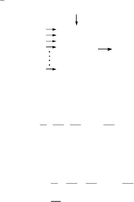
Basic Architecture of a D/A Converter
Continuous Time D/A Converter-
Voltage |
Vref |
Scaling |
DVref |
Output |
v |
OUT |
= KDV |
|
|
|
ref |
||||
References |
|
Network |
|
Amplifier |
|
|
|
|
|
|
|
|
|
|
|
Binary Switches
b0 b1 b2 |
bN-1 |
Clocked D/A Converter-
|
|
Vref |
|
|
|
b0 |
|
|
|
|
|
b1 |
|
|
|
|
|
b2 |
|
Digital |
Vout |
Sample V* |
|
|
|
to |
|||
|
Latch |
|
and |
out |
|
|
analog |
|
|
||
|
|
|
hold |
|
|
|
|
converter |
|
|
|
|
|
|
|
|
|
bN-1 |
|
|
|
|
|
|
|
Clock |
|
|
|

Allen and Holberg - CMOS Analog Circuit Design |
Page X.1-3 |
Classification of D/A Converters
Done by how the converter is scaled-
D/A Converters
|
Serial |
|
|
|
|
Parallel |
|
|
|
|
|
|
|
|
|
|
|
||
|
|
|
|
|
|
|
|
|
|
|
|
|
|
|
|
|
|
|
|
|
Charge |
|
|
Voltage |
|
Charge |
|
|
Current |
|
|
|
|
|
|
|
|
|
|
Voltage and Charge
Slow |
Fast |

Allen and Holberg - CMOS Analog Circuit Design |
Page X.1-4 |
Static Characterization of D/A Converters
Ideal input-output D/A converter Static Characteristic -
Analog Ouput Value
1.000 |
|
|
|
|
|
|
|
|
|
|
|
|
|
|
|
|
|
0.875 |
|
|
|
|
|
|
|
|
0.750 |
|
|
|
|
|
|
|
|
|
|
|
|
|
1 LSB |
|
|
|
0.625 |
|
|
|
|
|
|
|
|
|
|
Ideal |
|
|
|
|
|
|
|
|
|
analog |
|
|
|
|
|
0.500 |
|
|
output |
|
|
|
|
|
|
|
|
|
|
|
|
|
|
0.375 |
|
|
|
|
|
|
|
|
0.250 |
|
|
|
|
|
|
|
|
0.125 |
|
|
|
|
|
|
|
|
0.000 |
|
|
|
|
|
|
|
|
000 |
001 |
010 |
011 |
100 |
101 |
110 |
111 |
|
Digital Input Code
Vref
An ideal LSB change causes an analog change of 2N
Allen and Holberg - CMOS Analog Circuit Design |
Page X.1-5 |
Definitions
Resolution is the smallest analog change resulting from a 1 LSB digital change (quantified in terms of N bits).
Quantization Noise is the inherent uncertainty in digitizing an anlog value with a finite resolution converter.
Infinite resolution analog output - finite resolution analog output
0.5LSB |
|
|
|
|
|
VREF |
VREF |
|
|
|
|
|
0.5 |
= |
|
|
|
|
|
|
|
2N |
2N+1 |
|
|
|
|
|
|
Digital Input Code |
|
-0.5LSB |
|
|
|
|
|
VREF |
-VREF |
|
|
|
|
|
-0.5 |
= |
|
000 |
|
001 |
010 |
|
011 |
2N |
2N+1 |
Dynamic range (DR) |
is the ratio of FS to the smallest resolvable |
||||||
difference. |
|
|
|
2N − 1 |
|
|
|
|
|
|
VREF |
|
|
|
|
DR = |
|
FS |
2N |
= 2N − 1 |
|
||
LSB change |
= |
1 |
|
||||
|
|
|
V R E F 2N |
|
|
|
|
DR(dB) = 20 log10( 2 N − 1) |
6N dB |
|
|
||||
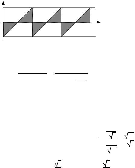
Signal to noise ratio (SNR) for a sawtooth waveform
Approximating FS = LSB(2N -1) LSB(2N),
|
|
|
|
|
2N |
|
|
|
|
|
|
SNR = |
Full scale RMS value |
= |
2 |
2 |
= |
12 |
2N |
|
|
||
|
RMS value of quantization noise |
|
|
1 |
2 |
2 |
|
|
|
||
|
|
|
|
|
|
|
|
|
|
||
|
|
|
|
|
|
12 |
|
|
|
|
|
|
|
6 |
|
|
6 |
|
|
|
|
N |
|
|
|
|
N |
|
2 |
|
+ 20 log10(2 |
) |
|||
SNR (dB) = 20 log10 |
2 2 |
= 20 log10 |
|
|
|||||||
= 20 log10(1.225) + 6.02N = 1.76 dB + 6.02N dB

Allen and Holberg - CMOS Analog Circuit Design |
Page X.1-6 |
Definitions - Continued
Full scale (FS) is the the maximum DAC analog output value. It is one LSB less than VREF .
2N − 1
FS = VREF 2N
A monotonic D/A (A/D) converter is one in which an increasing digital input code (analog input) produces a continuously increasing analog output value (digital output code).
Offset error is a constant shift of the actual finite resolution characteristic from the ideal infinite resolution characteristic.
Gain error is a deviation between the actual finite resolution characteristic and the ideal infinite resolution characteristic which changes with the input.
Integral nonlinearity (INL) is the maximum difference between the actual finite resolution characteristic and the infinite resolution characteristic.
Differential nonlinearity (DNL) is the maximum deviation of any analog
FS output changes caused by an input LSB change from its ideal change of 2N
.

Allen and Holberg - CMOS Analog Circuit Design |
Page X.1-7 |
3-BIT D/A CONVERTER ILLUSTRATION
|
VREF |
|
|
|
7 |
|
|
8 |
|
|
3 |
output |
|
4 |
|
5 |
|
analog |
VREF) |
8 |
2 |
||
Normalized |
(Ratioto |
1 |
3 |
||
|
|
8 |
1
4
1
8
0
000
0
Ideal D/A conversion
1 LSB 
Ideal analog output
001 |
010 |
011 |
100 |
101 |
110 |
111 |
|
1 |
2 |
3 |
4 |
5 |
6 |
7 |
8 |
8 |
8 |
8 |
8 |
8 |
8 |
8 |
8 |
Digital input, code and fractional value
Ideal relationship