

Статьи на перевод PVDF_P(VDF-TrFE) / article2
.pdfJournal of the Korean Physical Society, Vol. 51, No. 2, August 2007, pp. 719 722
The Ferroelectricity and Electrical Properties of P(VDF-TrFE)
Copolymer Film
Dong-Won Kim, Gwang-Geun Lee and Byung-Eun Park
Department of Electrical and Computer Engineering, University of Seoul, Seoul 130-743
(Received 9 November 2006)
Poly(vinylidene fluoride-trifluoroethylene)(P(VDF-TrFE)) copolymer thin films with a molar ratio of 75/25 have been studied to investigate their ferroelectricity. P(VDF-TrFE) solutions of 3, 7 and 10 wt% were fabricated on Si(100) substrates by using a spin-coating method. In order to achieve crystallization, we annealed the deposited films at 150 ◦C for one and half hours without any addional treatments, such as a heat-treatment, poling, or mechanical drawing. The thicknesses of the deposited films were 60, 170 and 400 nm for the 3, 7 and 10 wt% solutions, respectively. Hysteretic characteristics were observed in the capacitance-voltage (C-V) curves for Au/P(VDFTrFE)/Si diodes and may be considered to be due to the ferroelectric nature of the P(VDF-TrFE) films. The memory window width was measured at a low voltage below 1 V for a film coated with a 3 wt% solution. The memory window widths in this metal-ferroelectric-semiconductor (MFS) fabricated with 3, 7 and 10 wt% P(VDF-TrFE) solutions were about 1.2, 2.7 and 3.6 V for a bias sweep from –5 V to 5 V, respectively.
PACS numbers: 77.84.Jd
Keywords: Poly(vinylidene fluoride-trifluoroethylene), P(VDF-TrFE), Ferroelectric polymer, Memory window
I. INTRODUCTION
Since H. Kawai discovered the strong piezoelectricity in poly(vinylidene fluoride) (P(VDF)) in 1969, PVDF and its copolymer, poly(vinylidene fluoridetrifluoroethylene) (P(VDF-TrFE)), have been intensively studied for a wide range of applications, including nonvolatile memory in organic electronic devices, owing to their ferroelectricity, piezoelectricity and pyroelectricity [1,2]. PVDF has been reported to be crystallized variously into four types of crystalline phase (α, β, γ and δ). All types, except the α phase, form a polar phase. The spontaneous polarization of the γ and the δ phases was reported to be nearly half that of the β phase, and the α phase can be converted into the β phase by mechanical drawing or annealing under high pressure after high temperature annealing [3, 4]. On the other hand, P(VDF-TrFE) can easily form the β phase without an additional process by adding a small amount of TrFE. The copolymer exhibits much higher crystallinity than PVDF does. P(VDF-TrFE) can be directly crystallized into the β phase by heat treatment at a temperature between the Curie transition temperature (Tc) and the melting temperature (Tm) [5]. Yagi et al. reported that the size of the hydrogen atom is similar to that of fluorine; for that reason, VDF and TrFE are randomly dis-
E-mail: pbe@uos.ac.kr; Fax: +82-2-2249-6802
tributed to form the copolymer and are crystallized into a single crystalline phase analogous to the β phase PVDF [6]. In the copolymer of VDF and TrFE, the molar content of VDF controls the spontaneous polarization value. P(VDF-TrFE) with VDF of a 70 80 % exhibits high polarization while the crystal structure and crystallinity are decided by the content of TrFE [7,8].
Recently, there have been many studies on ferroelectric-gate field-e ect transistors (FeFETs) for nonvolatile memory devices [9]. A direct deposition of ferroelectrics on a Si substrate causes inter-di usion of constituents. As a consequence, a metal-ferroelectric- insulator-semiconductor (MFIS) structure with a bu er layer has been proposed [10]. On the other hand, because the P(VDF-TrFE) film is deposited at room temperature, such an inter-di usion does not matter. In this research, we deposited P(VDF-TrFE) thin films on silicon substrates and studied the ferroelectricity of the films by observing the capacitance-voltage (C-V) characteristics. The surfaces of the films were also observed by using a scanning electron microscope (SEM).
II. EXPERIMENT
The P(VDF-TrFE) copolymer powder with VDF 75 % and TrFE 25 % was dissolved in a dimethylformide (DMF) solvent. At the same time, three kinds of so-
-719-
-720- |
Journal of the Korean Physical Society, Vol. 51, No. 2, August 2007 |
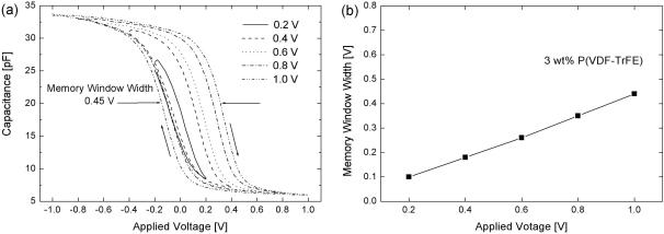
Fig. 1. (a) C-V characteristics for Au/P(VDF-TrFE)/Si diodes with a 3 wt% P(VDF-TrFE) film at 1 MHz and (b) Memory window width calculated from the C-V curves with respect to the applied voltage.
lutions were prepared with concentrations of 3, 7 and 10 wt%. P-type Si(100) wafers were used as substrates. After cleaning by using a standard process (acetone, methanol and de-ionized water), We dipped the substrates in a dilute HF solution to remove surface oxide. The thin films were deposited by using a spin-coating method. The deposited films were annealed on a hotplate at 150 ◦C for one and half hours because the melting and the Curie transition temperature were 150 ◦C and 120 ◦C, respectively. The thicknesses of the deposited films were about 60, 170 and 400 nm for 3, 7 and 10 wt%, respectively. The MFS structure of Au/P(VDF- TrFE)/p-Si was used to measure the ferroelectric properties. The top electrode with a diameter of 200 um was vacuum-evaporated. A topography image was obtained by using a scanning electron microscope (SEM). The capacitance-voltage (C-V) characteristics were measured by using a HP4280A C-V plotter.
III. RESULTS AND DISCUSSION
Figure 1 shows the C-V characteristics of the P(VDFTrFE)/Si structure measured at very low voltage and 1 MHz. The C-V curves were measured at a bias sweep range from ±0.2 V to ±1 V. The C-V plot showed a hysteresis loop, with a clockwise trace as indicated by the arrows in Figure 1. This loop indicated the ferroelectric behavior of the P(VDF-TrFE) film. Figure 1 shows the hysteresis loop was not yet saturated for a bias sweep voltage of ±0.2 V whereas for a bias sweep voltage above ±0.4 V, it was setting into saturation. The memory window width calculated from the C-V curves is summarized in Figure 1(b). The memory window width gradually was increased as the sweep voltage range increased from ±0.2 V to ±1 V. It is worth noting that the typical saturated ferroelectric hysteresis loops were obtained at a sweep voltage range of ±0.4 V. Reece et
al. reported good ferroelectric characteristics at an operating voltage of ±15 V for 170-nm-thick P(VDF-TrFE) (75/25) copolymer thin films fabricated on 100-nm-thick SiO2/Si structures (i.e., MFIS) by using the LangmuirBoldgett method [11]. The reasons for a saturated ferroelectric hysteresis loop at a very low operation voltage in our work as compared with results of Reece et al. can be attributed to our P(VDF-TrFE) (75/25) copolymer thin films being fabricated directly on silicon substrates and to the thickness of the thin films (60 nm) being relatively thin. It was very encouraging result that the hysteresis loop was saturated, and the memory window width was about 0.2 V at a sweep range of ±0.4 V. Thus, a new possibility exists for using this film in low-voltage memory devices operating at 0.4 V. Using the accumulation capacitance value, the relative dielectric constant of P(VDF-TrFE) film was estimated to be about 7.
Figure 2(a) shows the C-V characteristics when the 3 wt% P(VDF-TrFE) film was measured at a relatively high sweep range from ±1 V to ±5 V. The memory window width of the hysteresis loop was estimated to be 1.2 V, which is useful for device applications. At the same time, in order to make certain of the e ect of mobile ionic charges on the hysteresis loop, we changed the scanning speed of the bias voltage from 0.01 to 0.75 V/s in the C-V measurement. However, the memory window width did not change with the scanning speed range investigated. This suggests that the hysteresis characteristics resulted because of ferroelectricity of the P(VDF-TrFE) thin film. In the cases of the 7 and the 10 wt% P(VDFTrFE) films, the C-V characteristics are showed in Figs. 2(b) and (c). As compared with Figure 2(a), the memory window width is far wider than that of the 3 wt%. The variations of the memory window widths for 3, 7 and 10 wt% of the P(VDF-TrFE) are illustrated in Figure 3. The memory window widths were 1.2, 2.7 and 3.6 V for 3, 7 and 10 wt% P(VDF-TrFE) thin films when the sweep range was ±5 V. The memory window width gradually expanded, as the sweep range was increased.

The Ferroelectricity and Electrical Properties of P(VDF-TrFE)· · · – Dong-Won Kim et al. |
-721- |
Fig. 2. C-V characteristics for Au/P(VDF-TrFE)/Si diodes with a (a) 3, (b) 7 and (c) 10 wt% P(VDF-TrFE) thin film measured at 1 MHz as the voltage was swept from ±1 V to ±5 V.
Fig. 3. Memory window width (V) versus the applied voltage (V) for the various wt% solutions.
Figure 4 shows a SEM image of the 3 wt% P(VDFTrFE) thin film. As one can see from this image, surface lamellae were observed, and chain of molecules was ordered in a crystalline lamella. It is assumed that each chain of molecules instantaneously rotated in a crystalline lamella like a trunk of tree.
Fig. 4. The SEM image of the 3 wt% P(VDF-TrFE) thin film annealed at 150 ◦C for one and half hours.
IV. CONCLUSION
We fabricated P(VDF-TrFE) (75/25) thin films on a p-type Si(100) substrates by using a spin-coating method with 3, 7 and 10 wt% solution. The P(VDF-TrFE) films were annealed at 150 ◦C for one and half hours without any additional process, such as a heat-treatment, poling, or mechanical drawing. From the C-V measurements, hysteric curves were observed, implying the ferroelec-
-722- |
Journal of the Korean Physical Society, Vol. 51, No. 2, August 2007 |
tric nature of P(VDF-TrFE). Particularly, the 3 wt% P(VDF-TrFE) film showed a saturated hysteresis loop with a memory window width of 0.2 V at a very low sweep range of ±0.4 V. We conclude from these results that a copolymer of VDF and TrFE is one of the most promising candidates for a ferroelectric organic copolymer. We also found that this structure is a reliable means for achieving a low-cost, high-density, nonvolatile random access memory with a very low operating voltage.
REFERENCES
[1]H. Kawai, J. Appl. Phys. 8, 975 (1969).
[2]J. G. Bergman and J. H. McFee and G. R. Crane, Appl. Phys. Lett. 18, 203 (1971).
[3]K. Matsushige, K. Nagata and T. Takemura, Jpn. J. Appl. Phys. 17, 467 (1978).
[4]K. Kimura and H. Ohigashi, Appl. Phys. Lett. 43, 834 (1983).
[5]K. Koga and H. Ohigashi, J. Appl. Phys. 59, 2142 (1986).
[6]T. Yagi, M. Tatemoto and J. I. Sako, Polym. J. 12, 209 (1980).
[7]T. Furukawa, Phase Transitions 18, 143 (1989).
[8]E. H. Khalil, A. Ribbe, S. Isoda and K. Matsushige, Chem. Engin. Sci. 58, 397 (2003).
[9]B. E. Park and H. Ishiwara, Appl. Phys. Lett. 79, 806 (2001).
[10]B. E. Park, K. Takahashi and H. Ishiwara, J. Korean Phys. Soc. 46, 346 (2005).
[11]T. J. Reece, S. Ducharme, A. V. Sorokin and M. Poulsen, Appl. Phys. Lett. 82, 142 (2003).