

Статьи на перевод PVDF_P(VDF-TrFE) / Facile Preparation of Highly Oriented Poly(vinylidene fluoride)
.pdfArticle
pubs.acs.org/Macromolecules
Facile Preparation of Highly Oriented Poly(vinylidene fluoride) Langmuir−Blodgett Nanofilms Assisted by Amphiphilic Polymer Nanosheets
Huie Zhu, Masaya Mitsuishi,* and Tokuji Miyashita
Institute of Multidisciplinary Research for Advanced Materials (IMRAM), Tohoku University, 2-1-1 Katahira, Aoba-ku, Sendai 980-8577, Japan
*S Supporting Information
ABSTRACT: We describe a facile and novel method for preparing highly dense Langmuir−Blodgett (LB) nanofilms of poly(vinylidene fluoride) (PVDF) with precisely adjustable film thickness from several to hundreds of nanometers, assisted by amphiphilic poly(N-dodecylacrylamide) (pDDA) nanosheets. Even at a molar mixing ratio of PVDF:pDDA up to 50:1, the high collapse surface pressure of 44.4 mN/m obtained using this method is a breakthrough for the preparation of PVDF LB nanofilms, which is devoted to the resulting high-density PVDF nanofilms. As shown by FTIR and XRD measurements, the
mixed LB nanofilms without any postprocessing comprised dominant ferroelectric β phase of 95% and negligible paraelectric α phase. Furthermore, through control of the surface pressure, controllable PVDF crystal morphologies were achieved. Moreover, β phase PVDF dominates in all cases. After applying a dc bias of 5 V through a conductive cantilever, the local polarized pattern on the surface of a nine-layer mixed LB nanofilm observed using Kelvin probe force microscopy indicates that it is possible to induce all dipoles in one direction in the mixed LB nanofilm, which is promising for application in low-voltage nanoelectronics.
■ INTRODUCTION
Poly(vinylidene fluoride) (PVDF) and its copolymers have attracted much attention because of their excellent mechanical and chemical properties, especially their interesting electrical properties such as piezoelectricity discovered by Kawai in 19691 and pyroelectricity found by Bergman in 1971.2 Because they have such special properties, their applications to superhydrophobic materials,3,4 nonvolatile low-voltage memories,5−8 nanogenerators9 and even polymer bulk-heterojunction solar cells10 have been studied extensively.
PVDF and its copolymers are semicrystalline polymers, in which at least five molecular conformations can be found, including an alternating trans−gauche α phase (TGTG′), an all-trans β phase (TTTT), a partially polar γ phase (TTTGTTTG′), a partially polar δ phase (TGTG′), and a nonpolar ε phase (TTTGTTTG′).11−14 Of all the phases, the all-trans polar β phase with the largest spontaneous polarization is responsible for the ferroelectrics, but nonpolar α phase correlates to the paraelectrics, which indicates that it is crucial to enhance the content of β phase crystal as much as possible but suppress the α phase for better ferroelectricity.15 PVDF homopolymer has lower crystallinity of 50−60%,16 which decreases the content of β crystal to a limited degree, whereas β phase PVDF displays the largest dipole moment (≈2.1 D), which still makes PVDF homopolymer an extremely attractive material for piezoelectrics and pyroelectrics (Scheme 1a). To date, several methods have been carried out to produce β phase PVDF thin films or fibers, including mechanical stretching,17
Scheme 1. (a) Chemical Structure of PVDF and 3D Structure of All-Trans PVDF Molecular Conformation (Orange, F; Blue, H; Gray, C); (b) Chemical Structure of pDDA
electrical poling,18,19 thermal annealing,20,21 formation of composites with nanoclays,15,22−25 and crystallization induced by the hydrate salt.26,27 However, to obtain high-performance PVDF devices, the film thickness and roughness as well as the content of β crystals must be optimized.21,28
Received: August 13, 2012
Revised: October 23, 2012
Published: November 8, 2012
© 2012 American Chemical Society |
9076 |
dx.doi.org/10.1021/ma301711g | Macromolecules 2012, 45, 9076−9084 |

Macromolecules |
Article |
The Langmuir−Blodgett (LB) technique29−34 has been used for regular thin films with tunable film thickness and controllable packing structure using amphiphiles as well as nonamphiphilic molecules. The application of LB technique to nonamphiphilic conductive polymers such as regioregular poly(3-hexylthiophene) (P3HT) o ers a unique approach for constructing molecular devices.35 In addition, Ducharme et al. found ferroelectric vinylidene fluoride (VDF)−trifluoroethylene (TrFE) copolymer (p(VDF-TrFE)) can be dispersed onto the water surface to form a stable Langmuir film. Then they transferred such a Langmuir film onto substrates using the horizontal method (or the Langmuir−Schaefer (LS) method); the obtained ultrathin p(VDF-TrFE) LS nanofilms showed high order and enhanced dielectrics on a nanoscale.36−38 Recently, homopolymer PVDF LS nanofilm was prepared using the same horizontal method, for which it was claimed that hydrogen bonding between PVDF molecules and water contributed to formation of the β phase and the dipole orientation.39 The PVDF LS nanofilms were believed to have high content of β crystals. However, the annealing process made it di cult to ascertain whether such an annealing procedure caused the formation of the ferroelectric β crystal or not. Furthermore, the film density and film surface roughness are important factors for applications. These factors were seldom presented in previous works. More importantly, no related report describes real LB nanofilms of such ferroelectric polymers created using the vertical deposition method. In addition, no LB nanofilms of PVDF or its copolymers have been built.
In our previous work, a series of experimental results demonstrated that a nonamphiphilic functional monomer can be introduced into LB nanofilms by copolymerization with N-
dodecylacrylamide (DDA), which has excellent properties to form monolayers at the air−water interface.33,40−43 Moreover,
it has been reported that functional nonamphiphilic poly(3- hexylthiophene) LB nanofilms were fabricated by mixing with poly(N-dodecylacrylamide) (pDDA) (Scheme 1b) using superpurified water as the subphase at a mixing ratio of pDDA:P3HT = 1:4.44 Excellent monolayer stability and transfer properties
are caused by the hydrogen-bonding network between the amide groups in the pDDA molecules.34,44−46 By repeated
deposition, precise control of the thickness and homogeneity of the hybrid nanofilms in the nanoscale was achieved easily. Based on this building block, a variety of functional and novel hybrid nanomaterials were constructed and exploited for di erent applications.
In this work, we first prepare PVDF LB nanofilms using
vertical dipping with the aid of pDDA, obtaining the highest collapse pressure out of the reported values.36,47 The two
polymers can form a stable mixed Langmuir film at the air− water interface with increasing molar mixing ratios from 1:4 to 50:1 (PVDF:pDDA/n:n) at 20 °C, which can be transferred uniformly onto various substrates. Moreover, its transfer ratio reaches 0.90 even at the highest mixing ratio, measured using a quartz crystal microbalance (QCM). Without any posttreatment, the obtained nanofilms with precisely controllable film thickness showed rather high contents of PVDF β crystals demonstrated by Fourier transform infrared and X-ray di raction measurements. Prepared under surface pressure of 30 mN/m, the mixed LB nanofilms were observed with numerous fiber-like structures corresponding to its high density of 1.82 g/cm3. In addition, the local potential pattern
polarized by a conductive cantilever was demonstrated using Kelvin force microscopy (KFM).
■ EXPERIMENTAL SECTION
Materials. PVDF (Mn = 7.1 × 10⁴, Mw = 1.8 × 10⁵) was purchased from Aldrich and was reprecipitated once before use. pDDA (Mn = 3.0 × 10⁴, Mw = 8.9 × 10⁴) was synthesized through free radical polymerization initiated by AIBN referring to the previous method.45,48 The solvents including N-methyl-2-pyrrolidone (NMP) and chloroform were commercially available and used without further purification. Octyltrichlorosilane was purchased from Tokyo Chemical Industry Co. Ltd. for the hydrophobic treatment of the substrate surface.
Procedures of LB Deposition. PVDF and pDDA were dissolved respectively in NMP and chloroform at room temperature with the same solution concentration of ca. 1 mM. The two resultant solutions of pDDA and PVDF were then spread successively onto the water surface to form stable mixed Langmuir film at di erent molar mixing ratios of PVDF:pDDA from 0:1 to 50:1. The water was purified using an ultrapure water system (>17.5 MΩ cm, CPW-101; Advantec Toyo Kaisha Ltd.). Experiments for surface pressure (π)−area (A) isotherms and preparation of the mixed LB nanofilms were carried out using an automatically controlled Langmuir trough (FSD-220&21; U.S.I. Corp.) at a compression rate of 14 cm2/min at 20 °C. During deposition, the substrate holder was lifted at a dipping speed of 10 mm/min in both upstrokes and downstrokes. If not otherwise specified, mixed LB nanofilms with di erent ratios were prepared at a dipping speed of 10 mm/min at 20 °C under surface pressure of 30 mN/m and dried under a nitrogen flow. For the preparation of pure PVDF LS nanofilms, the substrate was fixed onto the holder with the surface horizontal to the Langmuir film on the water surface. One monolayer per cycle was deposited onto the substrate. The deposition condition was 10 mm/min lifting speed at 12 mN/m and 20 °C.
Measurements. The UV−vis absorption spectra were obtained using a UV−vis absorption spectrometer (U-3000; Hitachi Ltd.). The Fourier transform infrared (FTIR) transmission and reflection− absorption spectra (RAS) measurements were carried out at a spectral resolution of 4 cm−1 using FTIR (FTIR 4200; Jasco Corp.) under a nitrogen atmosphere using silicon wafer and gold-coated glass substrates, respectively. The mixed LB nanofilms were investigated using atomic force microscopy (AFM) measurements (SPA-400; Seiko Instruments Inc.) under di erent modes. The dynamic mode (DFM) was used for the surface topography. The contact mode was carried out to polarize the mixed LB nanofilms under a bias voltage using a conductive Pt-coated silicon cantilever (OMCL-AC240TM-B2; Olympus Corp.). Then, the Kelvin mode (KFM) was used to obtain the polarized potential images using the same cantilever. The quartz crystal microbalance (QCM) method was used to evaluate the transfer ability of the mixed Langmuir film onto substrates (CRO5-P; U.S.I. Corp.). The X-ray di raction pattern was measured using a di ractometer (D8 Advance; Bruker AXS K.K.) with a Cu Kα radiation source (λ = 0.154 nm). Quartz, silicon wafers, and glass were used as substrates for di erent measurements. Their hydrophilic treatment was done using a UV-O3 cleaner after being washed thoroughly using chloroform, acetone, and 2-propanol. Hydrophobic substrates were obtained by immersing the aforementioned hydrophilic ones into an octyltrichlorosilane chloroform solution for 3 h. For KFM and IR-RAS measurements, a 100 nm gold layer was thermally deposited onto a glass substrate.
■ RESULTS AND DISCUSSION
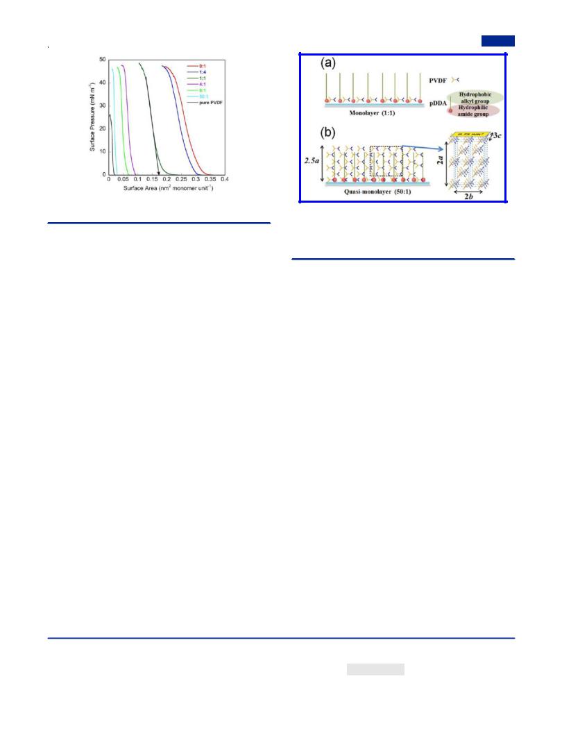
Formation of Mixed Monolayer and Quasi-Mono- layer. Figure 1 shows π−A isotherms of pure PVDF, pDDA, and their mixtures with various mixing ratios at 20 °C, from which a series of sharply rising curves with high collapse surface pressures are visible, indicating that all of them can form stable and compact mixed Langmuir film at the air−water interface. Even at a mixing ratio up to 50:1 (PVDF:pDDA), the collapsed
9077 |
dx.doi.org/10.1021/ma301711g | Macromolecules 2012, 45, 9076−9084 |
Macromolecules |
Article |
|
|
|
|
|
|
|
Figure 1. π−A isotherms of mixed monolayers containing PVDF and pDDA at di erent molar ratios of PVDF:pDDA at 20 °C.
surface pressure reached 44.4 mN/m, which is a breakthrough
in the preparation of PVDF and its copolymer LB nanofilms at high surface pressure.16,36,47,49 For pure PVDF, its collapse
pressure was much lower: about 25 mN/m. In addition, no phase separation occurred during the compression. Because of the strong hydrogen-bonding network between amide groups of pDDA backbone as well as the excellent amphiphilicity of pDDA,44 the stability of PVDF Langmuir film at the air−water interface was enhanced dramatically, making it possible to obtain highly dense PVDF LB nanofilms.
The average limiting surface area (Saver) is attained by extrapolating the linear portion of the condensed state in the
π−A isotherms to zero (Table 1).50 The values are within experimental errors of no more than 5%. The occupied area per DDA repeating unit (SDDA) is assumed as 0.28 nm2. Then the limiting surface area (SVDF) per VDF repeating unit at the air−
water interface was calculated using Saver = SVDFx + SDDA(1 − x), where x denotes the molar content of VDF repeating
units.44 At the lower mixing ratio, PVDF molecules were dispersed into the two-dimensional hydrogen-bonding network of pDDA to form a monolayer at the air−water interface (Figure 2a). However, the Saver decreased suddenly as the mixing ratio of PVDF:pDDA increased to 4:1, as shown in
Table 1, which accounts for the formation of densely packed PVDF orthorhombic β crystal,51,52 as verified by the following
FTIR and AFM measurements. According to the lattice parameters of PVDF β crystals (Figure 2b)6,52 and the
thickness of the mixed LB nanofilm at 50:1 (see below), we deduced that the mixed Langmuir film (50:1) at the air−water interface contains six PVDF molecular layers packed along the vertical direction with the molecular zigzag plane parallel to the water surface. In this case, the stable mixed Langmuir film at the air−water interface is not the real monolayer. Because of its good transfer ability, it is claimed to be the quasi-monolayer (Figure 2b). Furthermore, dividing the cross-sectional area of the crystal unit cell (0.75 nm2) in Figure 2b by the number of the repeated units (ca. 45) below this area in the quasimonolayer, the calculated value of SVDF was obtained as 0.017 nm2, which shows excellent agreement with the experimental
Figure 2. Schematic diagrams: (a) the monolayer (1:1); (b) the quasimonolayer (50:1) at the air−water interface with the PVDF backbones perpendicular to the paper plane and the crystal unit cell of β phase PVDF with a vertical polar b-axis and in-plane a- and c-axes (a = 0.858 nm, b = 0.491 nm, c = 0.256 nm).
value, 0.019 nm2, presented in Table 1. This result reveals that the PVDF molecules do take an in-plane orientation, as deduced.
Deposition Process of the Mixed LB Nanofilm. All the mixed Langmuir films at the air−water interface were transferred onto hydrophobic substrates as well as hydrophilic substrates to form Y-type mixed LB nanofilms at 20 °C. For hydrophobic substrates, film deposition was started from the first downstroke. However, when substrates were hydrophilic, the film adhered onto substrates starting from the upstroke of the first cycle. Dividing the decreased area of the quasimonolayer at the air−water interface for each stroke by the substrate area, the transfer ratio for the sample even at 50:1 was calculated respectively as 0.94 (downstrokes) and 1.0 (upstrokes). All deposition processes were carried out by lifting the holder down and up at a speed of 10 mm/min. However, pure PVDF is not available for preparing the mixed LB nanofilm by the vertical depositing method, irrespective of the Langmuir film forming ability, which suggests that pDDA tremendously improved the transfer properties of PVDF onto the substrates as well.
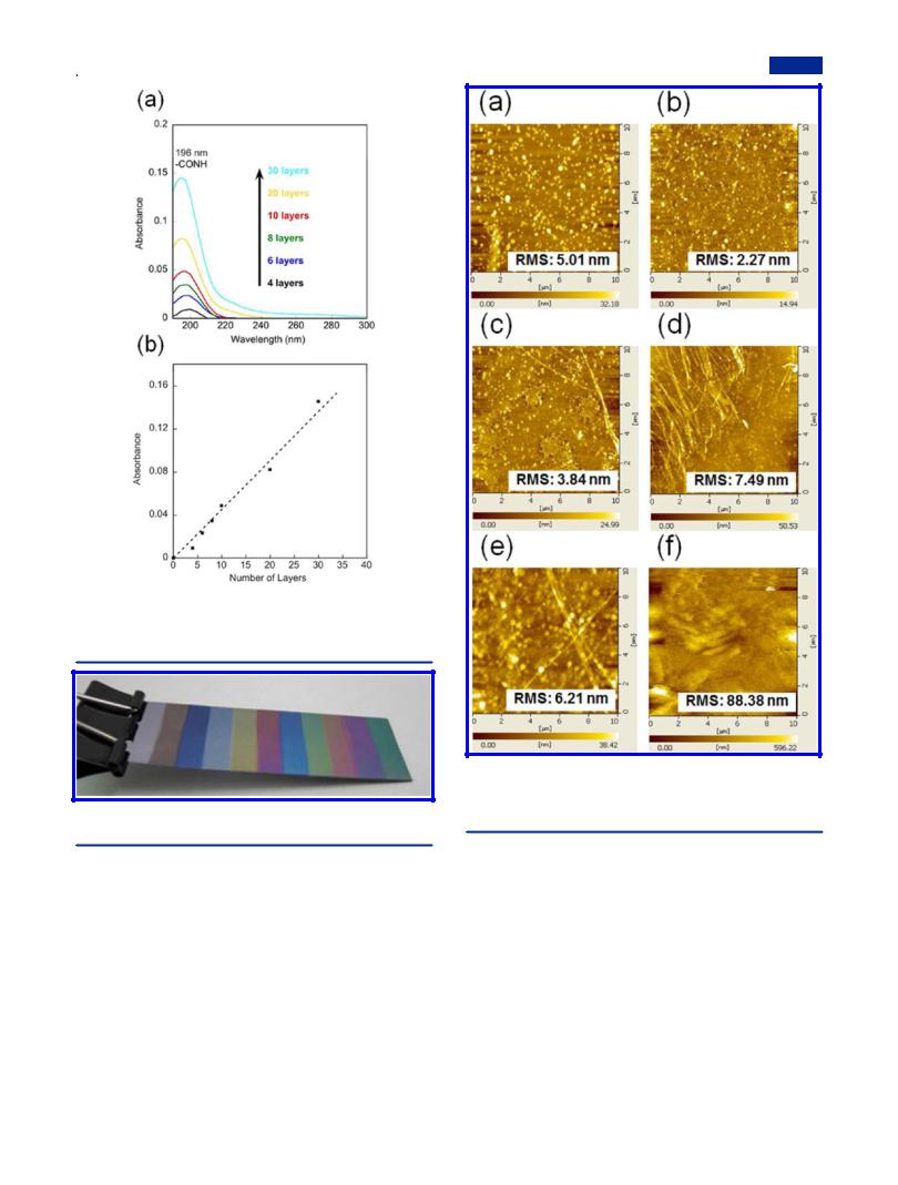
The UV absorption spectra of the mixed LB nanofilm at 50:1 are shown in Figure 3a. The absorption intensity at 196 nm from amide groups in pDDA molecules increases linearly along with the number of deposition layers (Figure 3b), which indicates that regular and uniform deposition was carried out even at a mixing ratio up to 50:1.44 The quasi-monolayer was also deposited on one hydrophobic silicon substrate from 0 layers to 200 layers according to an arithmetic sequence with a common di erence of 20 layers. A related photograph is presented in Figure 4, in which the beautiful interference colors prove the regular layer structure of the mixed LB nanofilms as well as the smooth film surface.33 In contrast, the LS film on the substrate (Figure S1) has a rather rough surface. It is more e ective to attain uniform PVDF nanofilms using the present LB method. Therefore, it is a promising method to fabricate
Table 1. Limiting Surface Area at Di erent Mixing Ratios
PVDF:pDDA |
0:1 |
1:4 |
1:1 |
4:1 |
8:1 |
50:1 |
1:0 |
Saver (nm2) |
0.28 |
0.28 |
0.18 |
0.078 |
0.056 |
0.024 |
0.015 |
SVDF (nm2) |
0 |
0.28 |
0.070 |
0.028 |
0.028 |
0.019 |
0.015 |
9078 |
dx.doi.org/10.1021/ma301711g | Macromolecules 2012, 45, 9076−9084 |
Macromolecules |
Article |
|
|
|
|
|
|
|
Figure 3. (a) UV−vis absorption spectra of the mixed LB nanofilms of PVDF:pDDA = 50:1 with di erent layers on the hydrophobic quartz substrates. (b) Absorbance of amide groups in the pDDA chain at 196 nm as a function of the number of layers.
Figure 4. Mixed LB nanofilms from 0 to 200 layers, starting from the left side.
traditional ferroelectric electronics with high performance and low leakage in the nanoscale, such as nanocapacitors, ferroelectric transistors, and so on.
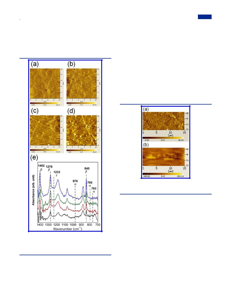
Surface Morphologies. Pure PVDF spread on the water surface can be transferred onto substrates at 12 mN/m using the horizontal deposition method (or LS method) to attain pure PVDF LS nanofilms. The surface morphologies of the mixed LB nanofilms as well as the pure PVDF LS nanofilm were obtained using AFM measurement in the DFM mode (Figure 5). The white spots of PVDF in the multilayer structure uniformly dispersed at a lower mixing ratio. However, when it reached a higher ratio than 4:1, PVDF crystallized to a marked degree, as shown in Figures 5c−e, which corresponds to the sudden decrease of Saver in Table 1. Fiber-like structures were formed spontaneously with increasing heights of 16.0 ± 2.0, 25.0 ± 3.0, and 30.0 ± 2.0 nm, respectively, correlating to the
Figure 5. AFM images of the 20-layer mixed LB nanofilms on hydrophobic silicon substrates. The mixing ratios of PVDF:pDDA are
(a) 1:4, (b) 1:1, (c) 4:1, (d) 8:1, (e) 50:1, and (f) the pure PVDF LS nanofilm.
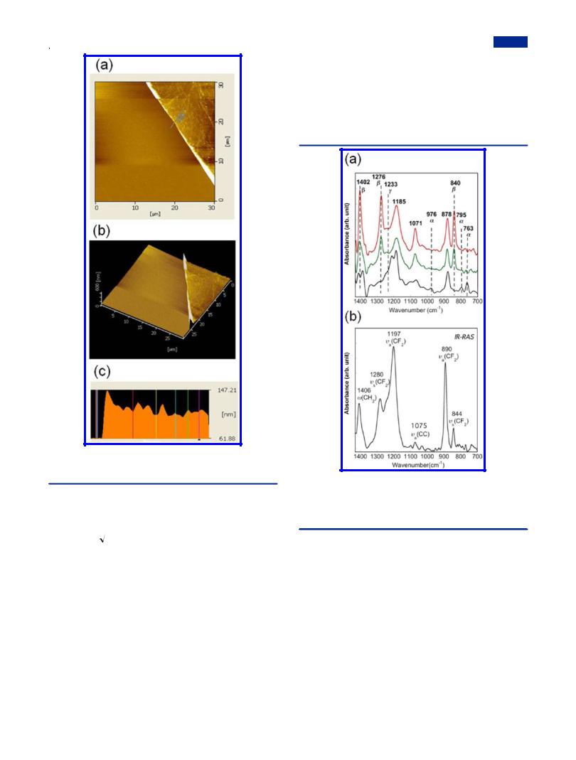
increasing density, which makes the root-mean-square (RMS) roughness of the mixed LB nanofilms exceed that of pDDA (less than 1.0 nm).53 For pure PVDF LS nanofilm (Figure 5f), the much larger roughness than those of mixed LB nanofilms proves that the improved transfer properties of PVDF were built with the aid of pDDA. The film thickness for the mixed LB nanofilms at 50:1 was estimated as 46.2 ± 3.0 nm for 20 layers according to the AFM images of the edge of the scratched area in Figure 6, which elucidates that the film deposition process is regular, with thickness of about 2.31 nm for each layer. In the following discussion, attention will be devoted to the mixed LB nanofilms at the highest mixing ratio (50:1) because we aim primarily at high β phase PVDF with content of pDDA down to a reasonable value if possible.
Transfer Ratio and Film Density. QCM method is an e ective means to measure the film change, in that mass
9079 |
dx.doi.org/10.1021/ma301711g | Macromolecules 2012, 45, 9076−9084 |
Macromolecules |
Article |
nanofilm thickness to be 2.31 nm from AFM images, corresponding to dense PVDF β crystals, which is 1.80 g/ cm3.55 According to the reported method,49 the crystallinity of the mixed LB nanofilms can be estimated as 52%, which is much higher than that of the original PVDF pellet, measured as 21% using di erential scanning calorimetry (DSC) (Figure S2).
Self-Orienting Behaviors of PVDF in the Mixed Nanofilms. Figure 7a shows FTIR spectra of PVDF casting
Figure 6. AFM images of a 20-layer mixed LB nanofilm (50:1) on a hydrophobic silicon substrate: (a) top view, (b) 3D image, (c) cross section.
changes result in frequency changes, as described by the Sauerbrey equation.54
|
2F 2 |
|
||
F = − |
|
0 |
m |
|
A |
μρ |
|||
|
|
|||
Therein, F stands for the change of frequency, F0 denotes the resonant frequency of the quartz resonator (= 9 MHz), A is the active vibrating area, μ signifies the shear modulus of quartz (= 2.947 × 10¹⁰ kg/(m s)), ρ represents the quartz density (= 2648 kg/m3), and m is the mass change. Because the measured average frequency change for depositing one-layer mixed LB nanofilm (50:1) under 30 mN/m is 76.8 Hz and because the electrode surface area of the quartz microbalance is 1.52 × 10⁻⁵ m2, the calculated mass change for one-layer deposition is 419.3 ng/cm2 using the Sauerbrey equation. In addition, the surface density of the quasi-monolayer obtained
from Saver is 466.8 ng/cm2 for the sample at PVDF:pDDA = 50:1. Therefore, the transfer ratio was calculated as 0.90, which
is consistent with the experimental results in the LB deposition process discussed earlier. Furthermore, the density of the mixed LB nanofilm is obtained as 1.82 g/cm3, assuming the one-layer
Figure 7. (a) FTIR spectra of di erent PVDF films: a casting PVDF film from PVDF/NMP solution (black line), 31-layer LS nanofilm of pure PVDF (green line), and 31-layer mixed LB nanofilm (50:1) (red line) on the silicon substrates. (b) IR-RAS spectrum of a 21-layer mixed LB nanofilm (50:1) on the gold-coated glass substrate.
film, pure PVDF LS nanofilm (31 layers), and the mixed LB nanofilm (31 layers) on silicon substrates. Well-known peaks at 763, 795, and 976 cm−1 are assigned to nonpolar α phase, and the β phase is associated with absorptions at 840, 1276, and
1402 cm−1. Then the peak at 1233 cm−1 is characteristic for the γ phase.15,56 In the mixed LB nanofilm and pure PVDF LS
nanofilm, the peaks for β phase at 840, 1276, and 1402 cm−1 are rather sharp. However, these peaks are absent in the FTIR spectrum of the casting film. In contrast, other peaks at 763 and 976 cm−1 for α phase and 1233 cm−1 for γ phase are negligible in the mixed LB nanofilm. We can conclude that the relative content of PVDF β crystals is improved robustly in the mixed LB nanofilm and pure PVDF LS nanofilm in comparison with the casting PVDF film; in contrast, α phase crystals were suppressed extensively. In the PVDF/NMP solution, the dipolar interaction and hydrogen bonding between PVDF and NMP molecules can preferably lead to better oriented
9080 |
dx.doi.org/10.1021/ma301711g | Macromolecules 2012, 45, 9076−9084 |
Macromolecules |
Article |
packing of CH2−CF2 dipoles.26 Although films of all three kinds were prepared from same PVDF solution in NMP, the self-orienting behavior in the LB and LS nanofilms indicates that the hydrogen-bonding interaction between PVDF and water molecules at the air−water interface played a key role in maintaining the oriented state of PVDF in NMP after spreading them onto the water surface.39 It is also noteworthy that the peak at 1402 cm−1 in the mixed LB nanofilm is a singlet, which is representative for β phase PVDF,56 whereas the doublet near 1400 cm−1 in the LS nanofilm is always seen in α phase.23 This finding indicates that the higher surface pressure for the deposition of the mixed LB nanofilm is more e ective for obtaining higher contents of PVDF β crystals.
The absorption band with dipole moments perpendicular to the film surface are expected to be enhanced, whereas the dipole moments nearly parallel to the film surface will be weakened in the IR-RAS spectra in comparison with those in the FTIR spectra.57 Moreover, the CF2 symmetric stretching mode at 1276 and 840 cm−1 (A1, μ//b) as well as the C−C asymmetric stretching mode at 1071 cm−1 and the CH2 wagging mode at 1402 cm−1 (B1, μ//c) in the FTIR spectrum of the mixed LB nanofilm (Figure 7a) become very weak in the IR-RAS spectrum (Figure 7b). In contrast, the absorption
bands of the CF2 asymmetric stretching at 1185 and 878 cm−1 (B2, μ//a) becomes much sharper.58,59 Furthermore, the lower
absorbance ratio of the A1 band to the B1 band, A844/A890 and A1280/A1197, in the present LB nanofilms in comparison with the reported value in ref 59 indicates that the trans-planar zigzag
chains tend to orient parallel to the substrate surface. The a- axes are oriented away from the substrate surface.59 Consequently, it can be concluded that in the mixed LB nanofilms the PVDF molecular zigzag plane (bc) is parallel to the substrate surface and that the a-axis of the PVDF crystals align normal to the substrate surface.
We also investigated the relation between the IR absorption intensity of the mixed LB nanofilms and the number of layers, as shown in Figure 8. The absorption intensity of β crystals at 1276 and 840 cm−1 increases sharply along with the increasing number of layers, which clearly shows the regular deposition of the quasi-monolayer attributable to the high stability and the wide-range regular structure of the quasi-monolayer. From this perspective, β phase PVDF with controllable thickness and area for di erent applications can be prepared easily using LB technique. However, to explore what impact will be brought to the mixed LB nanofilms by the annealing processing, the nanofilms were annealed at 135 °C for 2 h.56 Briefly, assuming that only α and β crystals can be found in the PVDF LB nanofilms, the relative fraction of β crystals can be calculated as follows:60
F(β) = |
Xβ |
= |
|
|
Aβ |
|
|
|
|
||
|
Xα + Xβ |
( |
Kβ |
)Aα + Aβ |
|
|
Kα |
||||
Therein, Xα and Xβ respectively represent the degree of crystallinity of each phase. Aβ and Aα represent the absorbance of α and β crystals at 766 and 840 cm−1. Kα and Kβ are the absorption coe cient at respective wavenumber, which are respectively 6.1 × 10⁴ and 7.7 × 104 cm2/mol. The resulting value of F(β) is up to 94.9% for the as-prepared PVDF mixed LB nanofilms with 40 layers. After annealing the sample, F(β) is still 94.7%. Therefore, the annealing process to enhance β crystals in the PVDF or its copolymer nanofilms reported earlier is unnecessary using the present method.
Figure 8. FTIR spectra of the mixed LB nanofilms (50:1) at di erent layers on the hydrophobic silicon substrates: 10 layers (black line), 20 layers (red line), 30 layers (green line), 40 layers (blue line); (a) before annealing; (b) after annealing at 135 °C for 2 h.
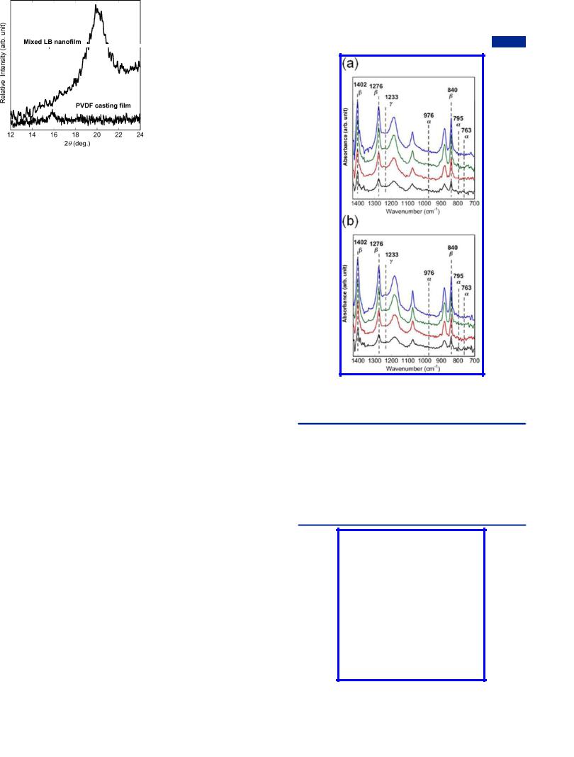
The XRD pattern further confirmed the dominant content of β crystals in the mixed LB nanofilm (50:1) shown in the FTIR spectra. As Figure 9 shows, the casting film of pure PVDF exhibits one peak at 2θ = 17.8°, corresponding to (100) reflection of α phase PVDF.61 In contrast, in the mixed LB nanofilm, only the ferroelectric phase at 2θ = 20.0° exists.62 The Bragg peaks, which usually ascribe to the regular layer
Figure 9. XRD patterns of a 40-layer mixed LB nanofilm (50:1) and a pure PVDF casting film on the hydrophobic silicon substrates.
9081 |
dx.doi.org/10.1021/ma301711g | Macromolecules 2012, 45, 9076−9084 |
Macromolecules |
Article |
structure in the mixed LB nanofilms,50 did not appear because fiber-like structures disrupt such regularity.
Controllable Crystal Morphologies of the Mixed LB Nanofilms. In this section, we explored the e ect of the depositing surface pressure on the film morphologies. The mixed LB nanofilms with 20 layers at a mixing ratio of 50:1 were prepared respectively at 3, 5, 20, and 30 mN/m onto the hydrophobic silicon substrates. Figure 10 shows their AFM
more e ective to eliminate α crystals and obtain dense β phase PVDF LB nanofilms at a higher deposition surface pressure. In addition, the single peak at 1402 cm−1 in the mixed LB nanofilm deposited under 30 mN/m is much sharper than in other cases, which proves further that a higher collapse surface pressure is useful to obtain not only highly dense PVDF nanofilms but also highly oriented PVDF nanofilms. Because of the much-enhanced collapse surface pressure of the PVDF quasi-monolayer, we realized facile adjustment on the crystal morphologies and content of β crystals over a very wide range in this work.
Electrical Properties. A two-step measurement was conducted to confirm the electrical properties of the resulting mixed LB nanofilms. First, a positive/negative bias voltage was applied to the conductive AFM cantilever under ambient conditions, making the sample surface polarized, which is called the prewriting procedure. Then, KFM mode was carried out to obtain images of polarized patterns at a lifting height of 20 nm, which is called the reading procedure.63,64 Figure 11 portrays
Figure 10. AFM images of the 20-layer mixed nanofilms (50:1) on the hydrophobic silicon substrates under di erent deposition surface pressure: (a) 3, (b) 5, (c) 20, and (d) 30 mN/m; (e) FTIR spectra of the four mixed LB nanofilms at 3 (black line), 5 (red line), 20 (green line), and 30 mN/m (blue line).
images and FTIR spectra, from which it is apparent that by controlling the depositing surface pressure, the mixed LB nanofilms with di erent crystal morphologies were obtained. Furthermore, all nanofilms are occupied by dominant β phase PVDF, as shown in Figure 10e. However, the relative higher α crystals content in the mixed LB nanofilms deposited under a lower surface pressure (3 and 5 mN/m) elucidates that it is
Figure 11. KFM images of a nine-layer mixed LB nanofilm (50:1) on the glass substrate coated with gold after charged by a positive bias of 5 V: (a) topographical image; (b) the surface potential image.
the topography and potential images of a nine-layer sample (50:1) on the glass substrate coated with a 100 nm gold layer after being charged by a bias of 5 V. The potential image shows us a pattern with the word “NANO”, which was written using the scan vector in the operation software of SPA-400. The polarized images, including the topography image and the potential image obtained after the prewriting procedure, prove that the dipole moment in the mixed LB nanofilms (ca. 21.6 nm) can be polarized to align in one direction at a voltage of 5 V (polarized electric field of ca. 230 MV/m). The polarized electric field is higher than the reported coercive field of β phase PVDF (75 MV/m).65 This higher field is the result of the special molecular orientation, and of the large interface e ect between the LB nanofilm and the metal electrode just as the case always happening in the PVDF copolymer.59 The introduction of pDDA into the resulting LB nanofilms is another factor contributing to the high coercive field. However, the future structure design is promising to decrease the coercive
field, which must make the PVDF LB nanofilms more e cient in the field of low-voltage polymer memory.28,66
9082 |
dx.doi.org/10.1021/ma301711g | Macromolecules 2012, 45, 9076−9084 |

Macromolecules |
Article |
■ CONCLUSIONS
A more versatile method to prepare dense PVDF LB nanofilms was realized, assisted by pDDA nanosheets, which have an excellent property of monolayer formation. This is the first report of the use of a vertical-dipping LB technique to acquire regular PVDF nanofilms. In the π−A isotherms of the mixed Langmuir films at the air−water interface, the rather high collapse surface pressure of PVDF quasi-monolayer at the mixing ratio of 50:1 is an important breakthrough compared with the reported value, which makes it successful to prepare highly dense PVDF LB nanofilms in this work. In addition, the mixed LB nanofilms obtained without any post-treatment were demonstrated with dominant ferroelectric phase and negligible paraelectric phase by FTIR spectra as well as the XRD patterns. Furthermore, the high transfer properties, controllable β crystal morphologies and film thickness, uniform film surface, and its electrical response ability must endow the mixed LB nanofilms with many applications as nanoelectronics such as highperformance memories, capacitors, transistors, and so on.
■ ASSOCIATED CONTENT
*S Supporting Information
Figures S1 and S2. This material is available free of charge via the Internet at http://pubs.acs.org.
■ AUTHOR INFORMATION
Corresponding Author
*E-mail: masaya@tagen.tohoku.ac.jp.
Notes
The authors declare no competing financial interest.
■ ACKNOWLEDGMENTS
The work was partially supported by a grant-in-aid for Scientific Research (B) (24350112) from the Japan Society for the Promotion of Science (JSPS). The work was also supported by the Nano-Macro Materials, Devices and System Research Alliance (MEXT) and the Research Seeds Quest Program (JST). In addition, we are grateful to Professor Hidetoshi Oikawa, IMRAM, Tohoku University, for the use of an X-ray di ractometer. The authors thank Mr. Yuta Hayasaka, IMRAM, Tohoku University, for assistance in XRD characterizations. The Central Analytical Facility of IMRAM is also acknowledged for providing the AFM instrument.
■REFERENCES
(1)Kawai, H. Jpn. J. Appl. Phys. 1969, 8 (7), 975−976.
(2)Bergman, J. G.; McFee, J. H.; Crane, G. R. Appl. Phys. Lett. 1971, 18 (5), 203−206.
(3)Zheng, Z. R.; Gu, Z. Y.; Huo, R. T.; Luo, Z. S. Appl. Surf. Sci. 2010, 256 (7), 2061−2065.
(4)Zhang, L.; Zha, D. A.; Du, T. T.; Mei, S. L.; Shi, Z. J.; Jin, Z. X. Langmuir 2011, 27 (14), 8943−8949.
(5)Park, Y. J.; Kang, S. J.; Lotz, B.; Brinkmann, M.; Thierry, A.; Kim, K. J.; Park, C. Macromolecules 2008, 41 (22), 8648−8654.
(6)Hu, Z. J.; Tian, M. W.; Nysten, B.; Jonas, A. M. Nat. Mater. 2009, 8 (1), 62−67.
(7)Kang, S. J.; Bae, I.; Shin, Y. J.; Park, Y. J.; Huh, J.; Park, S. M.; Kim, H. C.; Park, C. Nano Lett. 2011, 11 (1), 138−144.
(8)Park, Y. J.; Bae, I. S.; Kang, S. J.; Chang, J.; Park, C. IEEE Trans. Dielectr. Electr. Insul. 2010, 17 (4), 1135−1163.
(9)Chang, C. E.; Tran, V. H.; Wang, J. B.; Fuh, Y. K.; Lin, L. W. Nano Lett. 2010, 10 (2), 726−731.
(10)Yuan, Y. B.; Reece, T. J.; Sharma, P.; Poddar, S.; Ducharme, S.; Gruverman, A.; Yang, Y.; Huang, J. S. Nat. Mater. 2011, 10 (4), 296− 302.
(11)Lovinger, A. J. Macromolecules 1981, 14 (2), 322−325.
(12)Lovinger, A. J. Macromolecules 1982, 15 (1), 40−44.
(13)Lovinger, A. J. Science 1983, 220 (4602), 1115−1121.
(14)Gregorio, R.; Capitao,̃ R. C. J. Mater. Sci. 2000, 35 (2), 299−
306.
(15)Liu, Y. L.; Li, Y.; Xu, J. T.; Fan, Z. Q. ACS Appl. Mater. Interfaces 2010, 2 (6), 1759−1768.
(16)Zhu, L.; Wang, Q. Macromolecules 2012, 45 (7), 2937−2954.
(17)Calvert, P. Nature 1975, 256 (5520), 694−694.
(18)Wegener, M.; Gerhard-Multhaupt, R. IEEE Trans. Ultrason. Ferroelectr. Freq. Control 2003, 50 (7), 921−931.
(19)Arlt, K.; Wegener, M. IEEE Trans. Dielectr. Electr. Insul. 2010, 17
(4), 1178−1184.
(20)El Mohajir, B. E.; Heymans, N. Polymer 2001, 42 (13), 5661−
5667.
(21)Kang, S. J.; Park, Y. J.; Sung, J.; Jo, P. S.; Park, C.; Kim, K. J.; Cho, B. O. Appl. Phys. Lett. 2008, 92 (1), 012921.
(22)Priya, L.; Jog, J. P. J. Appl. Polym. Sci. 2003, 89 (8), 2036−2040.
(23)Buckley, J.; Cebe, P.; Cherdack, D.; Crawford, J.; Ince, B. S.;
Jenkins, M.; Pan, J. J.; Reveley, M.; Washington, N.; Wolchover, N. Polymer 2006, 47 (7), 2411−2422.
(24)Shah, D.; Maiti, P.; Gunn, E.; Schmidt, D. F.; Jiang, D. D.; Batt, C. A.; Giannelis, E. P. Adv. Mater. 2004, 16 (14), 1173−1177.
(25)Ramasundaram, S.; Yoon, S.; Kim, K. J.; Park, C. J. Polym. Sci., Part B: Polym. Phys. 2008, 46 (20), 2173−2187.
(26)He, X. J.; Yao, K. Appl. Phys. Lett. 2006, 89 (11), 112909.
(27)Li, X.; Chen, S. T.; Yao, K.; Tay, F. E. H. J. Polym. Sci., Part B: Polym. Phys. 2009, 47 (23), 2410−2418.
(28)Kang, S. J.; Park, Y. J.; Bae, I.; Kim, K. J.; Kim, H. C.; Bauer, S.; Thomas, E. L.; Park, C. Adv. Funct. Mater. 2009, 19 (17), 2812−2818.
(29)Feng, F.; Miyashita, T.; Okubo, H.; Yamaguchi, M. J. Am. Chem. Soc. 1998, 120 (39), 10166−10170.
(30)Swalen, J. D.; Allara, D. L.; Andrade, J. D.; Chandross, E. A.;
Garoff, S.; Israelachvili, J.; McCarthy, T. J.; Murray, R.; Pease, R. F.; Rabolt, J. F.; Wynne, K. J.; Yu, H. Langmuir 1987, 3 (6), 932−950.
(31)Mitsuishi, M.; Matsui, J.; Miyashita, T. Polym. J. 2006, 38 (9), 877−896.
(32)Zasadzinski, J. A.; Viswanathan, R.; Madsen, L.; Garnaes, J.; Schwartz, D. K. Science 1994, 263 (5154), 1726−1733.
(33)Kado, Y.; Mitsuishi, M.; Miyashita, T. Adv. Mater. 2005, 17 (15), 1857−1861.
(34)Taniguchi, T.; Yokoyama, Y.; Miyashita, T. Macromolecules 1997, 30 (12), 3646−3649.
(35)Xu, G. F.; Bao, Z. A.; Groves, J. T. Langmuir 2000, 16 (4), 1834−1841.
(36)Palto, S.; Blinov, L.; Bune, A.; Dubovik, E.; Fridkin, V.;
Petukhova, N.; Verkhovskaya, K.; Yudin, S. Ferroelectr. Lett. Sect. 1995, 19 (3−4), 65−68.
(37)Blinov, L. M.; Fridkin, V. M.; Palto, S. P.; Sorokin, A. V.; Yudin, S. G. Thin Solid Films 1996, 284−285, 469−473.
(38)Bune, A. V.; Fridkin, V. M.; Ducharme, S.; Blinov, L. M.; Palto,
S. P.; Sorokin, A. V.; Yudin, S. G.; Zlatkin, A. Nature 1998, 391 (6670), 874−877.
(39)Chen, S. T.; Li, X.; Yao, K.; Tay, F. E. H.; Kumar, A.; Zeng, K. Y. Polymer 2012, 53 (6), 1404−1408.
(40)Aminuzzaman, M.; Kado, Y.; Mitsuishi, M.; Miyashita, T. J. Mater. Chem. 2004, 14 (20), 3014−3018.
(41)Kim, Y.; Zhao, F.; Mitsuishi, M.; Watanabe, A.; Miyashita, T. J. Am. Chem. Soc. 2008, 130 (36), 11848−11849.
(42)Matsui, J.; Abe, K.; Mitsuishi, M.; Aoki, A.; Miyashita, T. Langmuir 2009, 25 (18), 11061−11066.
(43)Ishifuji, M.; Mitsuishi, M.; Miyashita, T. J. Am. Chem. Soc. 2009, 131 (12), 4418−4424.
(44)Matsui, J.; Yoshida, S.; Mikayama, T.; Aoki, A.; Miyashita, T. Langmuir 2005, 21 (12), 5343−5348.
(45)Miyashita, T. Prog. Polym. Sci. 1993, 18 (2), 263−294.
9083 |
dx.doi.org/10.1021/ma301711g | Macromolecules 2012, 45, 9076−9084 |

Macromolecules |
Article |
(46)Endo, H.; Kado, Y.; Mitsuishi, M.; Miyashita, T. Macromolecules 2006, 39 (16), 5559−5563.
(47)Ducharme, S.; Reece, T. J.; Othon, C. M.; Rannow, R. K. IEEE Trans. Dev. Mater. Reliab. 2005, 5 (4), 720−735.
(48)Miyashita, T.; Mizuta, Y.; Matsuda, M. Br. Polym. J. 1990, 22 (4), 327−331.
(49)Matsushige, K.; Takemura, T. J. Polym. Sci., Part B: Polym. Phys.
1978, 16 (5), 921−934.
(50)Mitsuishi, M.; Zhao, F.; Kim, Y.; Watanabe, A.; Miyashita, T. Chem. Mater. 2008, 20 (13), 4310−4316.
(51)Hayashi, S. I.; Imamura, A. J. Polym. Sci., Part B: Polym. Phys.
1992, 30 (7), 769−773.
(52)Bellet-Amalric, E.; Legrand, J. F. Eur. Phys. J. B 1998, 3 (2), 225−236.
(53)Endo, H.; Mitsuishi, M.; Miyashita, T. J. Mater. Chem. 2008, 18 (12), 1302−1308.
(54)Hanley, C. M.; Quinn, J. A.; Vanderlick, T. K. Langmuir 1994, 10 (5), 1524−1527.
(55)Hasegawa, R.; Kobayashi, M.; Tadokoro, H. Polym. J. 1972, 3 (5), 591−599.
(56)Shin, Y. J.; Kang, S. J.; Jung, H. J.; Park, Y. J.; Bae, I.; Choi, D. H.; Park, C. ACS Appl. Mater. Interfaces 2011, 3 (2), 582−589.
(57)Chen, H. Z.; Wang, M.; Yang, S. L. Thin Solid Films 1999, 357 (2), 208−213.
(58)Tashiro, K.; Kobayashi, M. Spectrochim. Acta, Part A 1994, 50 (8−9), 1573−1588.
(59)Park, Y. J.; Kang, S. J.; Park, C.; Lotz, B.; Thierry, A.; Kim, K. J.; Huh, J. Macromolecules 2008, 41 (1), 109−119.
(60)Gregorio, R.; Cestari, M. J. Polym. Sci., Part B: Polym. Phys. 1994,
32 (5), 859−870.
(61)Kim, G. H.; Hong, S. M.; Seo, Y. Phys. Chem. Chem. Phys. 2009, 11 (44), 10506−10512.
(62)Choi, J.; Borca, C. N.; Dowben, P. A.; Bune, A. V.; Poulsen, M.; Pebley, S.; Adenwalla, S.; Ducharme, S.; Robertson, L.; Fridkin, V. M.;
Palto, S. P.; Petukhova, N. N.; Yudin, S. G. Phys. Rev. B 2000, 61 (8), 5760−5770.
(63)Palleau, E.; Sangeetha, N. M.; Viau, G.; Marty, J. D.; Ressier, L. ACS Nano 2011, 5 (5), 4228−4235.
(64)Liscio, A.; Palermo, V.; Samorì, P. Acc. Chem. Res. 2010, 43 (4), 541−550.
(65)Ohigashi, H.; Hattori, T. Jpn. J. Appl. Phys. 1989, 28 (9), L1612−L1615.
(66)Nguyen, C. A.; Wang, J. L.; Chen, L.; Mhaisalkar, S. G.; Lee, P. S. Org. Electron. 2009, 10 (1), 145−151.
9084 |
dx.doi.org/10.1021/ma301711g | Macromolecules 2012, 45, 9076−9084 |