

Статьи на перевод PVDF_P(VDF-TrFE) / Control of Thin Ferroelectric Polymer Films
.pdfIEEE Transactions on Dielectrics and Electrical Insulation Vol. 17, No. 4; August 2010 |
1155 |
performance. Ferroelectric polymers contain the intrinsic defects arising from imperfect chain configuration, heterogeneous crystalline-amorphous boundaries, graingrain mismatches and residual solvent and these defects usually make it difficult to reduce film thickness drastically for low voltage operation. For FeFET memories with Si channel layers, thermally grown SiO2 interlayers were widely used. In an early work by Yamauchi, SiO2 layers were inserted at both gate/ferroelectric and semiconducting channel/ ferroelectric layer to reduce the gate leakage [98]. A recent work by Salvatore et al. reported a good top gate FeFET device with a P(VDF-TrFE) layer deposited on a thermally grown SiO2 layer. A FeFET with 40 nm thick P(VDF-TrFE) layer was operated at the voltage as low as 6 V with the good data retention capability up to a few days [107]. The high on/off drain current ratio over 105 was almost maintained after 105 endurance cycles programmed in the order of ms time scale.
Thermally curable PVP thin film has been used in a FeFET based on OTFT mainly due to its frequent usage in OTFT as a dielectric layer. We employed a thin PVP layer between vacuum deposited pentacene layer and a β-PVDF one in a FeFET device to provide a smooth interfacial surface on which the pentacene layer had a large crystalline domain with a proper crystal orientation for better hole mobility [115]. We have also confirmed that a PVP layer is effective for a pentacene FeFET with P(VDF-TrFE) in which the PVP layer was spin coated on the gate electrode in a bottom gate transistor structure. An approximately 100 nm thick PVP layer was also inserted between metal gate electrode and a P(VDFTrFE) layer to reduce the gate leakage current in a FeFET with single crystal TIPS-PEN as an active channel [129]. Our device was well operated at the sweeping voltage of ± 30V with good data retention longer than 15 hours. A PVP layer also allowed us to realize a low voltage operation at the voltage less than 15 V in a single crystal TIPS-PEN FeFET in which PVDF/PMMA blend ferroelectric layer was spin coated on the PVP layer to form bilayered gate insulator. Again good data retention longer than 15 hours was obtained in the device [130]. It is obvious that the polarization of all the ferroelectric layers we investigated were not fully saturated at the voltage applied because a significant amount of the voltage was shared with the dielectric PVP layer. Nevertheless, our devices exhibited the good data retention as well as long term stability over 200 days as explained in the previous section. Lim et al have also employed a PVP interlayer in a FeFET with ZnO active channel to obtain low leakage current between gate and drain electrode. More systematic study needs to be done for further understating the phenomena at the interface of the bilayer [127].
We have recently developed a new polymeric gate dielectric interlayer of a cross-linkable poly(styrene- random-methylmethacrylate) (P(S-r-MMA)) copolymer with a good thermal and chemical resistance in bottom gate
FeFET memory with pentacene active layer and P(VDFTrFE) one [153]. We chose the copolymer interlayer with the following reasons. First of all, good miscibility of PMMA with P(VDF-TrFE) insured the solid and firm interface with surface energy matched with each other. Secondly, a cross-linkable polymer was required because a polymeric interlayer should be chemically and thermally resistive to remain stable upon the spin coating and subsequent thermal annealing of a thin P(VDF-TrFE) layer. A thin uniform P(VDF-TrFE) film was successfully formed with well defined ferroelectric microdmains on an interlayer. Thickness of the interlayer turned out to be one of the most important factors for controlling gate leakage current which is supposed to be minimized for high ON/OFF bistability of a FeFET memory. We carefully controlled the film thickness ranging from 5 to 30 nm with the film roughness maintained. An interlayer inserted between gate electrode and P(VDF-TrFE) layer significantly reduces gate leakage current, leading to source-drain OFF current of approximately 10-11A in particular when its thickness becomes greater than approximately 25 nm as shown in Figure 16. A reliable FeFET device shows a clockwise I-V hysteresis with drain
current bistablility of 103 at ±40 V gate voltage. The types
and properties of interlayers employed in ferroelectric polymer memory elements are described in Table 4.
Figure 16. (a) Transfer characteristic curves (IDS-VG) at VD= -5 V of pentacene FeFETs with 6 different P(S-r-MMA) interlayers. (b) Plots of ON and OFF current as a function of the P(S-r-MMA) interlayer thickness. While ON current remains all similar, OFF current gradually decreases with the interlayer film thickness up to approximately 25 nm [153].

1156 |
Y. J. Park et al.: Control of Thin Ferroelectric Polymer Films for Non-volatile Memory Applications |
Table 4. Characteristics of ferroelectric memory devices with various inter layers.
Inter |
Device |
Thickness |
|
|
|
|
|
|
of PVDF- |
Major role of Interlayer |
Device characteristics |
Refs |
|||||
layers |
structure |
|||||||
TrFE (nm) |
|
|
|
|
|
|||
|
|
|
|
|
|
|
||
Inorganic |
|
|
|
|
|
|
|
|
|
|
|
|
|
|
|
||
SiO2 |
MFIS |
36~450 |
•Reduce leakage current |
• Operation voltage: ±15V at 1KHz |
•Operation voltage:±3V |
[100] |
||
|
|
|
|
• Threshold voltage shift: 2.8V |
|
•Nonferroelectric layer |
[102] |
|
|
|
|
|
Flatband voltage shift at –10 to +6 V |
formation |
[103] |
||
Ta2O5 |
MFIS |
100 |
•Reduce leakage current |
• Operation voltage: ±4V |
|
|
[77] |
|
|
|
|
•Prevent the shift of C-V curve |
• Memory window of 2.9V |
|
|
|
|
HfTaO |
MFIS |
46 |
•Reduce leakage current |
• Operation voltage: ±3V |
|
|
[105] |
|
|
|
(blended |
•Prevent the shift of C-V curve |
• Memory window width: 1.2V |
|
|
|
|
|
|
with PMMA) |
•Increase retention property |
• Data retention: 4hr |
|
|
|
|
|
|
|
|
|
|
|
|
|
Organic |
|
|
|
|
|
|
|
|
|
|
|
|
|
|
|
|
|
PEDOT |
MFIM |
65~210 |
• Low voltage operation |
Operation voltage ±5.2V |
|
|
[75] |
|
:PSS |
|
|
• Reduction of switching time |
Switching time : 103 times faster at 100Hz and 80MV/m than Al |
|
|||
|
|
|
|
electrode |
|
|
|
|
|
|
|
|
|
|
|
|
|
Ppy- |
MFIM |
50 |
• Increase of the crystallinity |
•Coercive voltage: 2.6 V |
|
|
[125] |
|
PSSH |
|
|
• Enhance the crystal dipole orientation |
•Switching time: 30 μs |
|
|
|
|
|
|
|
|
•Fatigue: more than 1x10⁷ cycles |
|
|
||
PEDOT |
MFIM |
50 |
• Low voltage operation |
• Coercive voltage: 2.6V |
|
|
[151] |
|
-PSSH |
|
|
• Enhanced fatigue property |
• 1x10⁷ of switching cycles |
|
|
|
|
SAMs |
MFIM |
30~250 |
• Preferred crystal orientation of a axis |
•Operation voltage: ±20V |
|
|
[140] |
|
|
|
|
perpendicular to CH3-terminated SAMs |
•Coercive voltage: 11.2V |
|
|
|
|
PTFE |
MFIM |
40 |
• Epitaxy with PVDF-TrFE crystals |
•1.7μC/cm2 at ±30V operation |
|
|
[148] |
|
|
|
|
-(010)PVDF-TrFE //(100)PTFE |
•Fatigue cycles of 5x10⁸ with 104Hz at ±20V |
|
|||
|
|
|
• Enhanced thermal hysteric behavior |
|
|
|
|
|
|
|
|
|
|
|
|
||
PVP |
MFIS |
100 |
•Prevent the shift of C-V curve |
• Operation voltage: ±30V |
• Retention: 40hr (25% reduction of |
[152] |
||
|
|
|
|
• Con/Coff ratio: 3.82 |
bistability) |
|
||
|
FeFET |
200~400 |
•Reduce gate leakage current |
• ZnO active layer |
• TIPS-PEN active layer |
[127] |
||
|
|
|
|
-operation voltage: ±40V |
- operation voltage: ±40V |
[129] |
||
|
|
|
|
-Ion/Ioff ratio: 104 |
- Ion/Ioff ratio: 5x10³ |
|
||
|
|
|
|
-gate leakage current 10-10A |
- retention property: 5x10⁴ sec |
|
||
|
|
|
|
|
- environmental stability >40days |
|
||
PVA |
MFIS |
200 |
•Prevent the shift of C-V curve |
• Operation voltage: ±30V |
• Con/Coff ratio: 4.076 |
[152] |
||
P(S- |
FeFET |
350 |
•Reduce gate leakage current |
• Operation voltage: ±40V |
|
|
[153] |
|
rMMA) |
|
|
|
• Enhanced Ion/Ioff ratio 102 times with over 25nm P(S-r-MMA) |
|
|||
3.4 PATTERNING OF FERROELECTRIC
POLYMERS
Micro/nanofabrication processes for ferroelectric polymers have been established not only for potentially realizing high density memory devices but also for understanding the structure-ferroelectric properties relation in the confined geometry. A direct pattern transfer technique was developed to form microstructures in the polymer film by photoetching using X-rays [154]. Upon increasing exposure to X-ray beam generated by synchrotron radiation source, a semimetallic photodegrated product was produced in P(VDF-TrFE) film prepared by LB method. The method was easily employed for micropatterning the ferroelectric film when combined with a nickel wire mesh mask, leading to regular arrays of ferroelectric domains of 16 μm in size. The same group also utilized X-ray source to fabricate micropatterned ferroelectric PVDF polymer vacuum-deposited on a Si substrate [155]. They also found the substantial chemical
modification of the PVDF film by the enhanced conjugation in the degraded polymer chains due to the loss of fluorine atoms. Alternating α and β type patterns were fabricated by laser ablation of a P(VDF-TrFE) film in which the irradiated region of an initial β P(VDF-TrFE) film was transformed into α due to thermally induced conformation change of the polymer [156].
Many attempts have been made to produce micropatterns by non-conventional soft lithographic techniques. Recently Hu et al have fabricated nanometer scale patterns of PVDF using nano-imprinting lithography [157]. The confined crystallization and resulting molecular ordering of α type PVDF crystals was successfully demonstrated in the nanoscopic trenches produced by nano-imprinting. The ordering of the PVDF crystals was attributed to the suppression of heterogeneous nucleation by the confinement as well as by partial chain alignment due to flow during the imprinting. Further understanding of the crystallization of PVDF in the confined geometry was made by Steinhart et al.
IEEE Transactions on Dielectrics and Electrical Insulation Vol. 17, No. 4; August 2010 |
1157 |
in which the confined crystallization of PVDF occurred inside nanopores of an anodized Al oxide membrane [158,159]. They revealed the 2D confinement again suppressed branching as well as spherulite formation and selected specific crystal orientation during growth. We utilized capillary molding technique and reported micron scale pattern formation of PVDF with controlled crystal orientation similar to ones of a PVDF confined in the 1D lines reported previously [160]. The previous works including ours, however, do not provide a practical patterning technique that produces isolated polar ferroelectric micro or nanodomains of PVDF because (1) the crystalline structure dealt with was nonpolar α type and (2) some polymer remained on the imprinted regions, resulting in non-isolated patterned domains.
We have recently demonstrated a micro-patterning technique that produces patterned arrays of isolated ferroelectric γ type domains embedded into non-polar α structure in thin PVDF films [139]. The method is based on using micro-imprinting of a spin cast α type PVDF film. The localized regions pressed by a patterned PDMS mold turn into polar γ type structure under certain temperature and pressure. We also reported that a capacitor fabricated with the pressed PVDF thin film showed reasonably high remanent polarization of approximately 6 μC/cm2, with the coercive voltage of approximately 11 V. The localized polar ferroelectric domains are successfully scaled down to a few hundred nanometers as shown in Figure 17.
(a)
500 nm
(b)
200 nm
Figure 17. (a) A SEM image of PVDF pattern with 2 μm circular holes fabricated by microimprinting process. The pressed regions look flat with ferroelectric γ crystals, while highly stretched α crystalline lamellae were seen in the un-pressed, elevated ones. The inset shows a schematic of the patterned arrays of ferroelectric γ crystals surrounded by the elevated non-polar α crystalline domains. (b) The elastomer with circular posts of 400 nm in diameter produced the isolated and indented ferroelectric PVDF pattern arrays as demonstrated with an AFM image [139].
We have also developed a method to fabricating ferroelectric alternating α and β-type PVDF line patterns on Au substrate based on micro-contact printing [115]. The substrate selective α and β crystal formation of PVDF film on Au substrate allowed us to fabricate micropatterned β crystals when a PVDF thin film was spin coated and subsequently annealed on a chemically patterned Au substrate with SAMs. A 250 nm thick PVDF film prepared on a microcontact printed Au substrate with COOH-terminated SAMs apparently displays a micropattern in which α type crystals were dominantly formed on COOH-treated regions while β crystals were on the bare Au regions.
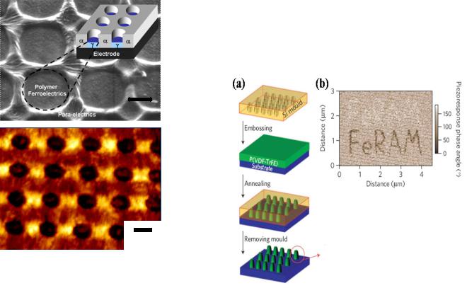
Microimprinting was employed to fabricate patterned arrays of a ferroelectric P(VDF-TrFE) film. Zhang et al presented the optimal microimprinting conditions of P(VDF-TrFE) thin films for high remanent polarization and high poling-induced surface potential [161]. Nanometer scale ferroelectric domains were fabricated of a P(VDFTrFE) film from LB method after annealing in the paraelectric phase. M. Bai et al have confirmed that the nanodomains retain the ferroelectric properties of the bulk material and thus be suitable for use in high density nonvolatile memory [162]. Recent work by Hu et al. has suggested that nanopatterned ferroelectric polymer domains were potentially useful not only for fabricating high integration density of cells larger than 33 Gbit/in2 but also for significantly reducing a coercive field to approximately 10 MV/m, well below previously reported bulk values [163]. Nano-imprinting technique allowed the preferential crystal orientation with very low level of structural defects in the patterned domains, leading to more uniform switching behavior from cell to cell as schematically depicted in Figure 18a.
Figure 18. (a) Schematic diagram of fabrication of high-density arrays of a P(VDF-TrFE) film by nanoimprinting process. (b) PFM piezo response phase of an array of P(VDF-TrFE) nanostructure fabricated by nanoimprinting [163].

1158 |
Y. J. Park et al.: Control of Thin Ferroelectric Polymer Films for Non-volatile Memory Applications |
Table 5. Critical design rules of materials and process components for ferroelectric polymer memory.
Components |
Properties |
Design rules |
Issues to be considered |
|
|
|
|
|
|
|
Degree of crystallinity |
as high as possible for high remanent |
~90% for PVDF-TrFE |
|
|
polarization |
~50% for PVDF |
||
|
|
|||
|
Orientation of crystals |
b axis aligned parallel to the electrode normal |
The orientation of ac plane on the electrode should |
|
|
be optimized. |
|||
|
|
|
||
Ferroelectric polymers |
Size of crystal domains |
as large as possible for good fatigue |
Film roughness should be minimized |
|
|
||||
|
Film thickness |
as thin as possible for low voltage operation |
Degree of crystallinity decreases with decrease of |
|
|
film thickness. |
|||
|
|
|
||
|
Dielectric constant |
as high as possible for low voltage operation |
~10 for both PVDF-TrFE and PVDF |
|
|
|
Nanocomposites with high k materials |
||
|
|
|
||
|
Dielectric constant |
as high as possible for low voltage operation |
High electric breakdown field is required |
|
Interlayers |
Film thickness |
as thick as possible for low leakage current |
Optimization is needed. |
|
|
||||
|
as thin as possible for low voltage operation |
|||
|
|
|
||
|
Conductivity |
as high as possible for low voltage operation |
Only a few Polymer conductors are suitable. |
|
|
and good fatigue |
|||
|
|
|
||
Semiconductors |
Field effect mobility |
as high as possible for high speed operation |
Less than the order of 1 cm2/Vs for most of organic |
|
and polymer semiconductors |
||||
|
|
|
||
|
|
|
|
|
Electrodes |
Source/drain |
work function matching with semiconductor |
Au is suitable for most of organic semiconductors |
|
Gate |
noble metals for high switching and good |
Depolarizing layer by the reaction with ferroelectric |
||
|
||||
|
fatigue |
polymers should not be formed. |
||
|
|
|||
Patterns |
Patterned domains |
as small as possible for high density memory |
Scalability |
|
Material damage during patterning process should |
||||
|
|
|
be minimized. |
Direct writing by surface probe microscope is known as an efficient way to fabricate a nanometer scale pattern surface of PVDF and P(VDF-TrFE) [69,70,164-166]. In particular piezoresponse force microscope (PFM) has been used to manipulate and image polarization of ferroelectric polymer films prepared by either LB method or spin coating and thus to achieve the polarization control with a resolution below 50 nm. For example, a P(VDF-TrFE) film by LB method exhibited a local hysteresis loop with the coercive voltage of approximately 10 V corresponding to macroscopic switching field of approximately 150 MV/m at 10 nm depth below the tip. This nanolithographic method is potential for high-density data storage and retrieval at densities exceeding 250 Gbit/in2. Furthermore, combined with polarization domain patterning, the domain-specific photoreduction reaction, which occurred in a metal ion solution under ultraviolet irradiation, enabled deposition of nanoparticles in complex configurations on the ferroelectric PVDF surface [166]. PFM was successfully employed to visualize the polarization switching of a nanopatterned P(VDF-TrFE) film fabricated by nanoimprinting, allowing the individually addressable patterned arrays as shown in Figure 18b [163].
Lateral modulation friction force microscope (LM-FFM) has been also useful not only for controlling the molecular orientation of P(VDF-TrFE) crystals but also potentially for
nanopatterning the thin films [142, 167]. Localized friction by a surface probe tip at high temperature induced the reorganization of polymer chains along the scanning direction, giving rise to well ordered ferroelectric crystalline edge-on lamellae aligned perpendicular to the tip-scan direction.
4 SUMMARY AND OUTLOOK
In this review article, we mainly focused on various material and process issues of thin ferroelectric polymers for nonvolatile ferroelectric polymer memory. In particular most of the article was devoted to describe the state of art in the development of memory devices based on PVDF and P(VDFTrFE). Followed by the overview of ferroelectric memory architectures, basic characteristics of ferroelectric polymers and various methods for sub micron film fabrication, the recent development of three main memory elements were in details elaborated such as MFM, MFIS, and FeFET with main emphasis on various memory functions including operating voltage, memory margin, fatigue, imprint, thermal budget and retention. In the last part, we discussed the challenging material and process issues for full realization of polymer ferroelectric memory which included (1) the control of polymorphic crystals, crystallization and crystal orientation,
(2) the control of interfaces of ferroelectric polymers with
IEEE Transactions on Dielectrics and Electrical Insulation Vol. 17, No. 4; August 2010 |
1159 |
metal and semiconductor and (3) the fabrication of patterned ferroelectric arrays. We comprehensively summarized the critical design rules for high performance non-volatile ferroelectric polymer memory in Table 5. It is commonly accepted that the device performance of ferroelectric polymer memories are yet to be critically compared with the leading edge memory devices based on inorganic materials. Further effort to establish the clear relationship between ferroelectric polymers and memory properties will be obviously required to advance the polymer memory technology in materials design, preparation, device fabrication and characterization. Nonvolatile memory based on ferroelectric polymers is, however, still promising by virtue of low cost, device flexibility, high performance and environmental compatibility. These unique characteristics make the ferroelectric memories attractive as an alternative or supplementary technology to the current memory technology. Among many other candidate organic and polymer memories based on the mechanisms such as resistive, charge trapping and transfer, and ionic conduction, ferroelectric polymer memory will in particular play a major role in the initial stage of development of this filed and thus find its way for the emerging applications in organic electronics combined with printing technology near future.
ACKNOWLEDGMENT
This work was supported by “SYSTEM2010” project and the 0.1 Terabit Non-volatile Memory Development funded by the Ministry of Commerce, Industry and Energy of the Korean Government, the Korea Science and Engineering Foundation(KOSEF) grant funded by the Korea government(MOST)(No. R11-2007-050-03001-0). We are also thankful for financial support from Samsung Electronics, Co., Ltd.
REFERENCES
[1]M.N. Kozicki, C. Gopalan, M. Balakrishnan, M. Park and M. Mitkova, “Non-Volatile Memory Based on Solid Electrolytes”, Non-Volatile Memory Technology Symposium, pp.10-17, 2004.
[2]S. Ducharme, T. J. Reece, C.M Othon, and R.K. Rannow, “Ferroelectric Polymer Langmuir-Blodgett Films for Nonvolatile Memory Applications”, IEEE Trans. Device and Materials Reliability, Vol. 5, pp. 720 – 735, 2005.
[3]J. C. Scott, and L.D. Bozano, “Nonvolatile Memory Elements Based on Orga0nic Materials”. Adv. Mater. Vol. 19, pp. 1452-1463, 2007.
[4]J. C. Scott, “Is There an Immortal Memory?” Science Vol. 304, pp. 6263, 2004.
[5]R.F. Service, “Organic Device Bids to Make Memory Cheaper”, Science, Vol. 293, pp. 1746, 2001.
[6]Y. Yang, L. Ma, and J. Wu “Organic Thin-Film Memory”, Materials Research Society Bulletin, Vol. 29, pp.833-837, 2004.
[7]A. Stikeman, “Polymer memory: the plastic path to better data storage”, Technol. Rev., Vol. 105, pp. 31, 2002.
[8]Mile long printed logic circuites for RFID tags. http://www.polyic.com/en/press-images.php; 2006
[9]B. Prince, Semiconductor Memories: a Handbook of Design, Manufacture, and Application, New York, Wiley, 1991.
[10]Q. Ling, D.-J. Liaw, E. Y. –H. Teo, C. Zhu, D. S.-H. Chan, E.-T. Kang, and K.-G. Neoh, “Polymer memories: Bistable electrical switching and device performance”, Polymer, Vol. 48, pp.5182-5201, 2007.
[11]Q. D. Ling, Y. Song, S.J.Ding, C.X.Zhu, D.S.H. Chan, D.L. Kwong, E.-T. Kang, and K.-G. Neoh, “Non-volatile polymer memory device based on a novel copolymer of N-vinylcarbazole and eu-complexed vinylbenzoate”, Adv. Mater., Vol. 17, pp.455-459, 2005.
[12]Q.D. Ling, W. Wang, Y. Song, C.X. Zhu, D.S.H. Chan, E.T. Kang, and K.-G. Neoh, “Bistable electrical switching and memory effects in a thin film of copolymer containing electron donor−acceptor moieties and europium complexes”, J. Phys. Chem. B. Vol. 110, pp.23995-24001, 2006.
[13]K. Takimoto, H. Kawade, E. Kishi, K. Yano, K. Sakai, K. Hatanaka, K. Eguchi, and T. Nakagiri, “Switching and memory phenomena in Langmuir–Blodgett films with scanning tunneling microscope”, Appl. Phys. Lett., Vol. 61, pp. 3032-3034, 1992.
[14]K. Yano, M. Kyogaku, R. Kuroda, Y. Shimada, S. Shido, H. Matsuda, Kiyoshi Takimoto, Otto Albrecht, Ken Eguchi, and Takashi Nakagiri, “Nanometer scale conductance change in a Langmuir-Blodgett film with the atomic force microscope” , Appl. Phys. Lett., Vol. 68, pp. 188-190, 1996.
[15]K. Sakai, H. Kawada, O. Takamatsu, H. Matsuda, K. Eguchi, T. Nakagiri, “Electrical memory switching in Langmuir-Blodgett films”, Thin Solid Films, Vol. 179, pp. 137-142, 1989.
[16]E.Y.H. Teo, Q.D.Ling, Y. Song, Y.P.Tan, W. Wang, E.T. Kang, D.S.H. Chan and Chunxiang Zhu, “Non-volatile WORM memory device based on an acrylate polymer with electron donating carbazole pendant groups” , Org. Electron. Vol. 7, pp. 173-180, 2006.
[17]A. Szymanski, D.C. Larson, and M. M. Labes, “A Temperatureindependent conducting state in tetracene thin film”, Appl. Phys. Lett., Vol. 14, pp 88-906, 1969.
[18]A.C. Arias, I.A.Huemmelgen, A. Meneguzzi, and C.A. Ferreira, “A conjugated polymer-based voltage-regulator device”, Adv. Mater., Vol. 9, pp. 972-974, 1997.
[19]T. Furukawa, “Ferroelectric Properties of vinylidene fluoride copolymers”, Phase Transit. Vol. 18, pp. 143-211, 1989.
[20]A. J. Lovinger, “Ferroelectric Polymers”, Science, Vol. 220, pp 11151121, 1983.
[21]Q. D. Ling, S. L. Lim, Y. Song, C. X. Zhu, D. S. H. Chan. E. T. Kang, and K.-G. Neoh, “Nonvolatile Polymer Memory Device Based on Bistable Electrical Switching in a Thin Film of Poly(N-vinylcarbazole) with Covalently Bonded C60”, Langmuir Vol. 23, pp 312-319, 2007.
[22]Y. Song, Q.D. Ling, S.L. Lim, E.Y.H. Teo. Y.P. Tan, L. Li, E. T. Kang, D. S. H. Chan, and C. Zhu, “Electrically Bistable Thin-Film Device Based on PVK and GNPs Polymer Material”, IEEE Electron Device Lett., Vol. 28, pp. 107-110, 2007.
[23]B. Pradhan, S.K. Batabyal, and A. J. Pal, “Electrical Bistability and Memory Phenomenon in Carbon Nanotube-Conjugated Polymer Matrixes”, J. Phys. Chem. B, Vol. 110, pp.8274-8277, 2006.
[24]Q. Ling, D. –J. Liaw, C. Zhu, D.S.H. Chan, E.-T. Kang, and K. –G. Neoh, “Polymer electronic memories: Materials, devices and mechanisms”, Progress in Polymer Sci., Vol. 33, 917-978, 2008.
[25]Y. Yang, J. Ouyang, L.P. Ma, R.J. Tseng and C.W. Chu, “Electrical Switching and Bistability in Organic/Polymeric Thin Films and Memory Devices” , Adv. Funct. Mater., Vol. 16, pp. 1001–1014, 2006.
[26]R. G. Kepler and R. A. Anderson: “Ferroelectric Polymers,” Advanced in Physics, Vol. 41, pp. 1-57, 1992.
[27]T. T. Wang, J. M. Herbert, and A. M. Glass, The Applications of Ferroelectric Polymers Glasgow, Blackie, U.K., 1988.
[28]H.S. Nalwa, Ferroelectric Polymers: Chemistry, Physics and Applications, New York, Marcel Dekker, 1995.
[29]A. F. Devonshire, Theory of ferroelectrics, Adv. Phys., Vol. 3, pp, 85130, 1954.
[30]M.E. Lines and A. M. Glass, Principles and Applications of Ferroelectrics and Related Materials, Oxford, U.K., Clarendon, 1977.
[31]N. Setter, D. Damjanovic, L. Eng, G. Fox, S. Gevorgian, S. Hong, A. Kingon, H. Kohlstedt, N.Y. Park, G. B. Stephenson, I. Stolitchnov, A.K. Taganstev, D.V. Taylor, T. Yamada, and S. Streiffer, “ Ferroelectric Thin Films: Review of Materials, Properties, and Applications”, J. Appl. Phys., Vol. 100, pp. 051606-1-051606-46, 2006.
[32]A. Sheikholeslami, and P.G. Gulak: “A Survey of Circuit Innovations in Ferroelectric Random-Access Memories”, Proc. IEEE, Vol. 88, pp. 667689, 2000.
[33]T. Sumi, N. Moriwaki, G. Nakane, T. Nakakuma, Y. Judai, Y. Uemoto, Y. Nagano, S. Hayashi, M. Azuma, E. Fujii, S.I. Katsu, T. Otsuki, L. McMillan, C. Paz de Araujo, and G. Kano, “A 256 kb
1160 |
Y. J. Park et al.: Control of Thin Ferroelectric Polymer Films for Non-volatile Memory Applications |
Nonvolatile Ferroelectric Memory at 3 V and 100 ns”, Digest of Technological Papers, IEEE Intern. Solid State Circuits Conf., pp. 268269, 1994.
[34]S. S. Eaton, D. B. Butler, M. Parris, D. Wilson, and H. McNeillie, “A Ferroelectric Nonvolatile Memory”, Digest of Technological Papers, IEEE Intern. Solid State Circuits Conf.,Vol. 130, pp. 130-131,1988.
[35]J. Evans and R. Womack, “An Experimental 512-bit Nonvolatile Memory with Ferroelectric Storage Cell”, IEEE J. Solid State Circuits , Vol.23, pp. 1171-1175, 1998.
[36]R. Womack and D. Tolsch, “A 16 kb Ferroelectric Nonvolatile Memory with a Bit Parallel Architecture”, Digest of Technological Papers, IEEE Intern. Solid State Circuits Conf., Vol. 351, pp. 242-243, 1989.
[37]T. Hayashi, Y. Igarashi, D. Inomata, T. Ichimori, T. Mitsuhashi, K. Ashikaga, T. Ito, M. Yoshimaru, M. Nagata, S. Mitarai, H. Godaiin, T. Nagahama, C. Isobe, H. Moriya, M. Shoji, Y. Ito, H. Kuroda, and M. Sasaki “A Novel Stack Capacitor Cell for High Density FeRAM
Compatible with CMOS Logic”, Technology Digest, IEEE Intern. Electron Devices Meet, pp. 543 – 546, 2002.
[38]H. McAdams, R. Acklin, T. Blake, D. Xiao-Hong, J. Eliason, J. Fong, W.F. Kraus, D. Liu, S. Madan, T. Moise, S. Natarajan, Ning Qian, Yunchen Qiu, K.A. Remack, K.A. J. Rodriguez, Roscher, A. Seshadri, and S.R. Summerfelt, “A 64-Mb Embedded FRAM Utilizing a 130-nm 5LM Cu/FSG Logic Process”, IEEE J. Solid State Circuits, Vol. 39, pp. 667 – 677, 2004.
[39]T. S. Moise, S. R. Summerfelt, H. McAdams, S. Aggarwal, K.R. Udayakumar, F.G. Celii, J.S. Martin, G. Xing, L. Hall, K.J. Taylor, T.Hurd, J. Rodriguez, K. Remack, M.D. Khan, K. Boku, G. Stacey, M. Yao, M.G.Albrecht, E. Zielinski, M. Thakre, S. Kuchimanchi, A. Thomas, B. McKee, J. Rickes, A. Wang, J. Grace, J. Fong, D. Lee, C. Pietrzyk, R. Lanham, S.R. Gilbert, D. Taylor, J. Amano, R. Bailey, F. Chu, G. Fox, S. Sun, and T. Davenport, “Demonstration of a 4 Mb, High Density Ferroelectric Memory Embedded within a 130 nm, 5 LM Cu/FSG Logic Process”, Technology Digest, IEEE Intern. Electron Devices Meet, pp. 535-538, 2002.
[40]S. Lee and K. Kim, “Current Development Status and Future Challenges of Ferroelectric Random Access Memory Technologies”, Jap. J. Appl. Phys. 45, pp. 3189-3193, 2006.
[41]K. Sugibuchi, Y. Kurogi, and N. Endo, “Ferroelectric Field-effect
Memory Device Using Bi4Ti3O12 film” , J. Appl. Phys., Vol. 46, pp 2877 – 2881, 1975.
[42]A. Kingon, P. Muralt, N. Setter, and R. Waser, Ceramic Materials for Electronics, edited by R. E. Buchanan, Dekker, New York, USA, pp. 465– 526, 2004.
[43]H. T. Lue, C. J. Wu, and T. Y. Tseng, “Device Modeling of Ferroelectric Memory Field-effect transistor for the Application of Ferroelectric Random Access Memory”, IEEE Trans. Ultrasonics, Ferroelectrics and Frequency Control, Vol. 5, pp. 5-14, 2003.
[44]S. L. Miller and P. J. McWhorter, “Physics of the Ferroelectric Nonvolatile Memory Field Effect Transistor”, J. Appl. Phys., Vol. 72, pp. 5999-6010, 1992.
[45]H. Ishiwara, “Current status and prospects of FET type ferroelectric memories”, J. Semicon. Technol. Sci. Vol. 1, 1-14, 2001.
[46]I. M. Ross, “Semiconductive translating device”, U.S. Patent, No. 2791760, 1957.
[47]J. L. Moll and Y. Tarui, “A New Solid State Memory Resistor”, IEEE Trans. Electron Devices, Vol. 10, pp. 338-339. 1963.
[48]S. Y. Wu, “A New Ferroelectric Memory Device, Metal-Ferroelectric- Semiconductor Transistor”, IEEE Trans. Electron Devices, Vol. 21, pp. 499-504, 1974.
[49]T. P. Ma, and J. Han, “Why is Nonvolatile Ferroelectric Memory Field-Effect Transistor Still Elusive?”, IEEE Electron Device Letters, Vol. 23, pp. 386-388, 2002.
[50]Y. Arimoto and H. Ishiwara, “Current Status of Ferroelectric Random-Access Memory”, Materials Research Society Bulletin, Vol. 29, pp. 823-828, 2004.
[51]H. Ishiwara, “Current Status of Fabrication and Integration of Ferroelectric-Gate FET's”, Material Research Soc. Symp. Proc., Vol. 596, pp. 427, 2000.
[52]K. Takahashi, K. Manabe, A. Morioka, T. Ikarashi, T. Yoshihara, H. Watanabe, and T. Tatsumi, “Abstracts of the International Conference Solid State Devices and Materials, Tokyo, Japan, (unpublished)” No. 1-2, 2004.
[53]H. Kohlstedt and H. Ishiwara, in Nanoelectronics and Information Technology: Advanced Electronic Materrial and Novel Devices, edited by R. Waser (Wiley-VCH, Weinheim), pp. 387, 2002.
[54]Q. M. Zhang, H. Xu, F. Fang, Z.-Y. Cheng, and F. Xia: “Critical Thickness of Crystallization and Discontinuous Change in Ferroelectric Behavior with Thickness in Ferroelectric Polymer Thin Films”, J. Appl. Phys., Vol. 89, pp. 2613-2616, 2001.
[55]F. Xia, H. Xu, F. Fang, B. Razavi, Z.-Y. Cheng, Y. Lu, B. Xu, and Q. M. Zhang, “Thickness Dependence of Ferroelectric Polarization Switching in Poly(vinylidene fluoride–trifluoroethylene) Spin Cast Films”, Appl. Phys. Lett., Vol. 78, pp. 1122-1124, 2001.
[56]Q. Gao and J. I. Scheinbeim: “Dipolar Intermolecular Interactions, Structural Development, and Electromechanical Properties in Ferroelectric Polymer Blends of Nylon-11 and Poly(vinylidene fluoride)”, Vol. 33, pp. 7564-7572, 2000.
[57]Y. Tajitsu, K. Ishida, S. Kanbara, H. Ohigashi, M. Date, and E. Fukada, “Temperature Dependence of Switching Characteristics in Polyurea-5 Thin Films”, Jpn. J. of Appl. Phys., Vol. 37, No. 9B, pp. 53755378, 1998.
[58]G. Scherowsky, Ferroelectric liquid crystal polymers. Nalwa HS editor, In Ferroelectric Polymers: Chemistry, Physics and Applications. New York; Marcel Dekker; pp. 435-538, 1995.
[59]R. G. Kepler and R. A. Anderson, “Ferroelectricity in Polyvinylidene Fluoride”, J. Appl. Phys., Vol. 49, pp. 1232-1235, 1978.
[60]A. J. Lovinger, Poly(vinylidene fluoride)” Developments in Crystalline Polymers-I, D. C. Basset, Ed. London, U.K.: Applied Sciences, pp. 195-273, 1981.
[61]A. J. Lovinger, “Ferroelectric transition in a copolymer of vinylidene fluoride and tetrafluoroethylene”, Macromolecules, Vol. 16, pp. 15291534, 1983.
[62]A. J. Bur, J. D. Barnes, and K. J. Wahlstrand, “A study of thermal depolarization of poly(vinylidene fluoride) using X-ray pole figure observations”, J. Appl. Phys. Vol. 59, pp.2345-2354, 1986.
[63]D. Naegele and D. Y. Yoon, “Orientation of crystalline dipoles in poly(vinylidene fluoride) films under electric field”, Appl. Phys. Lett., Vol. 33, pp.132-134, 1978.
[64] H. Evey-Aharon, T. J. Sluckin, P. L. Taylor, and A. J. Hopfinger, “Kink propagation as a model for poling in poly(vinylidene fluoride)”, Phys. Rev. B, Vol. 21, pp.3700-3707, 1980.
[65]K. Noda, K. Ishida, T. Horiuchi, K. Matsushige, and A. Kubono, “Structures of vinylidene fluoride oligomer thin films on alkali halide substrate”, J. Appl. Phys., Vol. 86, pp. 3688-3693, 1999.
[66]K. Noda, K. Ishida, A. Kubono, T. Horiuchi, H. Yamada, and K. Matsushige, “Structures and ferroelectric natures of epitaxially grown vinylidene fluoride oligomer thin films”, Jpn. J. Appl. Phys., Vol. 39, pp. 6358-6363, 2000.
[67]K. Noda, K. Ishida, A. Kubono, T. Horiuchi, H. Yamada, and K. Matsushige, “Molecular ferroelectricity of vinylidene fluoride oligomer investigated by atomic force microscopy” , Jpn. J. Appl. Phys. Part 1, Vol. 40, pp. 4361-4364, 2001
[68]K. Noda, K. Ishida, A. Kubono, T. Horiuchi, H. Yamada, and K. Matsushige, “Remanent Polarization of Evaporated Films of Vinylidene Fluoride Oligomers”, J. Appl. Phys., Vol. 93, pp. 2866-2870, 2003.
[69]A. Matsumoto, S. Horie, H. Yamada, K. Matsushige, S. Kuwajima, and K. Ishida, “ Ferroand piezoelectric properties of vinylidene fluoride oligomer thin film fabricated on flexible polymer film”, Appl. Phys. Lett., Vol. 90, pp. 202906-202906-3, 2007.
[70]S. Nozaki, K. Ishida, A. Matsumoto, S. Horie, S. Kuwajima, H. Yamada, and K. Matsushige, “Characterization of ferroelectric/metal interface under the repeated polarization switching”, Thin Solid Film, Vol. 516, pp. 2450-2453, 2008.
[71]A.C. Rastogi, and S.B. Desu, “Ferroelectric Poly(vinylidene Fluoride) Thin Film Grown by Low-Pressure Chemical Vapor Polymerization”, Chemical Vapor Deposition, Vol. 12, pp. 742-750, 2006.
[72]A.V. Bune, V.M. Fridkin, S. Ducharme, L.M. Blinov, S.P. Palto, A.V. Sorokin, S.G. Uudin, and A. Zlatkin, “Two-dimensional ferroelectric films”, Nature, Vol. 391, pp. 874-877,1998.
[73]R. C. G. Naber, B. de Boer, P. W. M. Blom, and D. M. de Leeuw, “Low-voltage Polymer Field-effect Transistors for Nonvolatile Memories”, Appl. Phys. Lett., Vol. 87, pp. 203509-1–203509-3, 2005.
[74]H. Xu, J. Zhong, X. Liu, J. Chen, and D. Shen, “Ferroelectric and switching behavior of poly(vinylidene fluoride-trifluoroethylene)
IEEE Transactions on Dielectrics and Electrical Insulation Vol. 17, No. 4; August 2010 |
1161 |
copolymer ultrathin films with polypyrrole interface”, Appl. Phys. Lett., Vol. 90, pp. 092903-1 – 092903-3, 2007.
[75]R. C. G. Naber, P. W. M. Blom, A.W. Marsman, and D. M. de Leeuw, “Low voltage switching of a spin cast ferroelectric polymer”, Appl. Phys. Lett., Vol. 85, pp. 2032-2034, 2004.
[76]F. Xia, B. Razavi, H. Xu, Z. –Y. Cheng, and Q. M. Zhang, “Dependence of Threshold Thickness of Crystallization and Film Morphology on Film Processing Conditions in Poly(vinylidene fluoridetrifluoroethylene) Copolymer Thin Films”, J. Appl. Phys., Vol. 92, pp. 3111-3115, 2002.
[77]S. Fujisaki, H. Ishiwara, and Y. Fujisaki, “Low-voltage operation of ferroelectric poly(vinylidene fluoride-trifluoroethylene) copolymer capacitors and metal-ferroelectric- insulator-semiconductor diodes”, Appl. Phys. Lett., Vol. 90, pp. 162902-1 – 162902-3, 2007.
[78]Y. J. Park, S. J. Kang, C. Park, K. J. Kim, H. S. Lee, M. S. Lee, U. Chung, and I. J. Park, “Irreversible extinction of ferroelectric polarization in P(VDF-TrFE) thin films upon melting and recrystallization“, Appl. Phys. Lett., Vol. 88, pp. 242908-1 – 242908-3, 2006.
[79]N. Tsutsumi, S. Yoda, and W. Sakai, “Infrared Spectra and Ferroelectricity of Ultra-thin Films of Vinylidene fluoride and trifluoroethylene Coploymer”, Polym. Int., Vol. 56, pp. 1254-1260, 2007.
[80]H. Xu, S. Ni, and C. Yang, “High Polarization Levels in Poly(vintlidene fluoride-trifluoroethylene) Ferroelectric Thin Films Doped with Diethyl Phthalate”, J. Appl. Polym. Sci., Vol. 88, pp. 1416-1419, 2003.
[81]S. Sakai, M. Date, and T. Furukawa, “Development of polarization Distribution in Fatigued Films of Ferroelectric Vinylidene Fluoride/Trifluoroethylene Copolymer”, Jpn. J. Appl. Phys., Vol. 41, pp. 3822-3828, 2002.
[82]G. Zhu, Z. Zeng, L. Zhang, and X. Yan, “Polarization fatigue in ferroelectric vinylidene fluoride and trifluoroethylene copolymer films”, Appl. Phys. Lett., Vol. 89, pp. 102905-1 – 10292905-3, 2006.
[83]F. Fang, W. Yang, and M. Z. Zhang, “Electric Fatigue in Poly(Vinylidene fluoride-trifluoroethylene) 68/32 Copolymer Films under Cyclic Electric Field”, J. Appl. Phys., Vol. 101, p. pp. 044902-1 – 044902- 5, 2007.
[84]G. Zhu, Z. Zeng, Q. Zhang, X. Yan, and R. Liu, “ Observation of asymmetric ferroelectric switching in fatigued ferroelectric vinylidene fluoride and trifluoroethylene copolymer films”, J. Appl. Phys. Vol. 103, pp. 084125-1-084125-6, 2008.
[85]G. Zhu, J. Zhang, X. Luo, and X. Yan, “Microscopic characterization of Polarization Fatigue in Ferroelectric vinylidene fluoride and trifluoroethylene Copolymer Films”, Org. Electron., In Press, 2009.
[86]T. Furukawa, T. Nakajima, and Y. Takahashi, “Factors Governing Ferroelectric Switching Characteristics of Thin VDF/TrFE Copolymer Films”, IEEE Transactions on Dielectrics and Electrical Insulation, Vol. 13, pp.1120-1131, 2006.
[87]Y. Tajitsu, “Effects of Thickness on Ferroelectricity in Vinylidene Fluoride and Trifluoroethylene Copolymers”, Jpn. J. Appl. Phys., Vol. 34, pp. 5418-5423, 1995.
[88]T. Furukawa, M. Date, M. Ohuchi, A. Chiba, “Ferroelectric Switching Characteristics in a Coplymer of Vinylidene Fluoride and Trifluoroethylene”, J. Appl. Phys., Vol. 56, pp. 1481-1486, 1984.
[89]S. Ducharme, V. M. Fridkin, A. V. Bune, S. P. Palto, L. M. Blinov, N. N. Petukhova, and S. G. Yudin, “Intrinsic Ferroelectric Coercive Field”, Phys. Rev. Lett, Vol. 84, pp. 175-178, 2000.
[90]A. M. Bratkovsky, and A. P. Levanyuk, “Comment on: “Intrinsic Ferroelectric Coercive Field”, Phys. Rev. Lett, Vol. 87, p. 019701-1, 2001.
[91]R. L. Moreira, “Comment on Intrinsic Ferroelectric Coercive Field”, Phys. Rev. Lett, Vol. 88, No. 17, p. 179701-1, 2002.
[92]R. C. Naber, P. W. M. Blom, D. M. de Leeuw, “Comment on ‘Extrinsic Versus Intrinsic Ferroelectric Switching: Experimental Investigations using Ultra-Thin PVDF Langmuir-Blodgett Films’”, J. Phys. D: Appl. Phys., Vol. 39, pp. 1984-1986, 2006.
[93]T. Nakajima, Y. Takahashi, and T. Furukawa, “Pulse Train Measurement of Ferroelectric Switching in Thin Films of Vinylidene fluoride/Trifluoroethylene Copolymer”, Appl. Phys. A, Vol. 91, pp. 33-39, 2008.
[94]F. Xia, and Q. M. Zhang, “Schottky emission at the metal polymer interface and its effect on the polarization switching of ferroelectric poly(vinylidene fluoride-trifluoroethylene) copolymer thin films“, Appl. Phys. Lett., Vol. 85, pp. 1719-1721, 2004.
[95]B. S. Kang, J.-G. Yoon, D. J. Kim, T. W. Noh, T. K. Song, Y. K. Lee, J. K. Lee, and Y. S. Park, “Mechanisms for retention loss in ferroelectric
Pt/Pb(Zr0.4Ti0.6)O3/Pt capacitors”, Appl. Phys. Lett., Vol. 82, pp.2124-2126 ,2003.
[96]B. S. Kang, D. J. Kim, J. Y. Jo, and T. W. Noh, J.-G. Yoon, T. K. Song, Y. K. Lee, J. K. Lee, S. Shin, and Y. S. Park, “Polarization retention
in Pb(Zr0.4Ti0.6)O3 capacitors with IrO2 top electrodes”, Appl. Phys. Lett., Vol. 84, pp. 3127-3129, 2004.
[97]Y. J. Park, J. Chang, S. J. Kang, and C. Park, “Polarization Retention of Thin Ferroelectric Poly(vinylidene fluoride-co-trifluoroethylene) Film capacitors”, Appl. Phys. Lett., Vol. 95, pp. 102902-1-102902-3, 2009.
[98]N. Yamauchi, “A Metal-Insulator-Semiconductor (MIS) Device Using a Ferroelectric Polymer Thin Film in the Gate Insulator”, Jpn. J. Appl. Phys., Vol. 25, pp. 590-594, 1986.
[99]N. Yamauchi, K. Kato, T. Wada, “Observation of Ferroelectricity in Very Thin Vinylidene Fluoride Trifluoroethylene Copolymer[P(VDF-
TrFE)] Films by High Frequency C-V Measurement of Al-SiO2-P(VDF- TrFE)-SiO2-Si Capacitors”, Jpn. J. Appl. Phys., Vol. 23, pp. L671-L673, 1984.
[100]T. J. Reece, S. Ducharme, A. V. Sorokin, M. Poulsen, “Nonvolatile memory element based on a ferroelectric polymer Langmuir–Blodgett film “, Appl. Phys. Lett., Vol. 82, pp. 142-144, 2003.
[101]A. Gerber, H. Kohlstedt, M. Fitsilis, R. Waser, T. J. Reece, S. Ducharme, and E. Rijie, “Low-voltage Operation of Metal-Ferroelectric- Insulator-Semiconductor Diodes Incorporating a Ferroelectric Polyvinylidene fluoride Copolymer Langmuir-Blodgett Film”, J. Appl. Phys. Vol. 100, pp. 024110-1 - 024110-5, 2006.
[102]S. H. Lim, A. C. Rastogi, and S. B. Desu, “Electrical Properties of Metal-Ferroelectric-Insulator-Semiconductor Structures Based on Ferroelectric Polyvinylidene Fluoride Copolymer Film Gate for Nonvolatile Random Access Memory Application”, J. Appl. Phys., Vol. 96, pp. 5673-5682, 2004.
[103]K. Henkel, I. Lazareva, D. Mandal, I. Paloumpa, K. Muller, Y.
Koval, P. Muller, and D. Schmei β er, “Electrical Investigations on
Metal/Ferroelectic/Insulator/Semiconductor Structures using Poly(vinylidene fluoride trifluoroethylene) as Ferroelectric Layer for Organic nonvolatile Memory Applications”, J. Vac. Sci. Technol. B., Vol. 27, pp. 504-507, 2009.
[104]S. Fujisaki, H. Ishiwara, Y. Fujisaki, “Organic Ferroelectic Diodes with Long Retention Characteristics Suitable for Non-Volatile Memory Applications”, Appl. Phys. Express, Vol. 1, pp.081801-1 - 081801-3, 2008.
[105]X. Lu, J. Yoon, and H. Ishiwara, “Low-voltage Operation and Excellent Data Retention Characteristics of Metal-Ferroelectric-Insulator- Si Devices based on Organic Ferroelectric Films”, J. Appl. Phys., Vol. 105, pp. 084101-1- 084101-4, 2009.
[106]T. Furukawa, S. Kanai, A. Okada, Y. Takahashi, and R. Yamamoto, “Ferroelectric switching dynamics in VDF-TrFE copolymer thin films spin coated on Si substrate” J. Appl. Phys., Vol. 105, pp. 061636-1-061636-7, 2009.
[107]G. A. Salvatore, D. Bouvet, I. Stolitchnov, N. Setter, and A. M. Ionescu, “Low voltage ferroelectric FET with sub-100 nm copolymer P(VDF-TrFE) gate dielectric for non-volatile 1T memory”, Solid State Device Research Conf., ESSDER, 38th European, pp. 162-165, 2008.
[108]R. Schroeder, L. A. Majewski, M. Grell, “ All-Organic Permanent Memory Transistor Using an Amorphous, Spin-Cast Ferroelecric-like Gate Insulator”, Adv. Mater., Vol. 16, pp. 633 – 636, 2004.
[109]K. N. N. Unni, R. de Bettignies, S. Dabos-Seignon, and J. Nunzi, “A nonvolatile memory element based on an organic field-effect transistor”, Appl. Phys. Lett., Vol. 85, pp. 1823-1825, 2004.
[110]Y. Matsuo, T. Ijicji, H. Yamada, J. Hatori, and S. Ikehata, “Electrical properties and memory effect in the field effect transistor based on organic ferroelectric insulator and pentacene”, Central Eurpean J. Phys., Vol. 2, pp. 357 – 366, 2004.
[111]C. A. Nguyen, P. S. Lee, and S. G. Mhaisalkar, “Investigation of Turn-on Voltage Shift in Organic Ferroelectric Transistor with High Polarity Gate Dielectric”, Org. Electron., Vol. 8, pp. 415-422, 2007.
[112]C. A. Nguyen, S. G. Mhaisalkar, and P. S. Lee, “Enhanced Organic Ferroelectric Field Effect Transistor Characteristics with Strained Poly(vinylidene fluoride-trifluoroethylene) Dielectric”, Org. Electron., Vol. 9, pp. 1087-1092, 2008.

1162 |
Y. J. Park et al.: Control of Thin Ferroelectric Polymer Films for Non-volatile Memory Applications |
[113]C. A. Nguyen, J. Wang, L. Chen, S. G. Mhaisalkar, and P. S. Lee, “Low-Voltage Organic Ferroelectric Field Effect Transistors using Langmuir-Schaefer Films of Poly(vinylidene fluoride-trifluoroethylene)”, Org. Electron., Vol. 10, pp. 145-151, 2009.
[114]K. H. Lee, G. Lee, K. Lee, M. S. Oh, and S. Lim, “Flexible Low Voltage Nonvolatile Memory Transistors with Pentacene Channel and Ferroelectric Polymer”, Appl. Phys. Lett., Vol. 94, p. 093304-1 – 093304- 3, 2009.
[115]S. J. Kang, Y. J. Park, J. Sung, P. S. Jo, C. Park, K. J. Kim, and B. O. Cho,”Spin cast ferroelecric beta poly(vinylidene fluoride) thin films via rapid thermal annealing”, Appl. Phys. Lett., Vol. 92, pp. 012921-1 – 012921-3, 2008.
[116]B. Singh, N. Marjanovic, G. J. Matt, S. Gunes, N. S. Sariciftci, R. Schwodiauer, and S. Bauer, “Nonvolatile Organic Field-effect Transistor Memory Element with a Polymeric Gate Electret”, Appl. Phys. Lett., Vol. 85, pp. 5409-5411, 2004.
[117]T. B. Singh, N. Marjanovic, P. Stadler, M. Auinger, G. J. Matt, S. Gunes, N. S. Sariciftci, R. Schwodiauer, and S. Bauer, “Fabrication and Characterization of Soluble-processed Methanofullerene-based Organic Field-effect Transistors”, J. Appl. Phys., Vol. 97, pp. 083714-1 - 083714- 5, 2005.
[118]B. Singh, N. Marjanovic, N. S. Sariciftci, R. Schwodiauer, and S. Bauer, “Electrical Characteristics of Metal-insulator-semiconductor Diodes and Transistors with Space Charge Electret Insulators: Towards Nonvolatile Organic Memories”, IEEE Trans. Dielectrics Electr. Insul., Vol. 13, pp. 1082-1085, 2006.
[119]K. Baeg, Y. Noh, J. Ghim, S. Kang, H. Lee, and D. Kim, “Organic Non-Volatile Memory Based on Pentacene Field-Effect Transistors Using a Polymeric Gate Electret”, Adv. Mater., Vol. 18, pp. 3179-3183, 2006.
[120]G. Gu, M. G. Kane, J. E. Doty, and A. H. Firester, “Electron Traps and Hysteresis in Pentacene-based Organic Thin-film Transistors”, Appl. Phys. Lett., Vol. 87, pp. 243512-1- 243512-3, 2005.
[121]R. C. G. Naber, C. Tanase, P. W. M. Blom, G. H. Gelinck, A. W. Marsman, F. J. Touwslager, S. Setayesh, and D. M. de Leeuw, “HighPerformance solution-processed polymer ferroelectric field-effect transistor”, Nat. Mater., Vol. 4, pp.243248, 2005.
[122]R. C. G. Naber, P. W. M. Blom, G. H. Gelinck, A. W. Marsman, and D. M. de Leeuw, “An Organic Field-effect Transistor with Programmable Polarity”, Adv. Mater., Vol. 17, pp. 2692-2695, 2005.
[123]R. C. G. Naber, M. Mulder, B. de Boer, P. W. M. Blom, and D. M. de Leeuw, “High Charge Density and Mobility in Poly(3-hexylthiophene) using a Polarizable Gate Dielectric”, Org. Electron., Vol. 7, pp. 132-136, 2006.
[124]F. A. Yildirim, C. Ucurum, R. R. Schliewe, R. M. Meixner, H. Goebel, and W. Krautschneider, “Spin-cast composite gate insulation for low driving voltages and memory effect in organic field-effect transistors”, Appl. Phys. Lett., Vol. 90, pp. 083501-1 – 083501-3, 2007.
[125]G. H. Gelinck, A. W. Marsman, F. J. Touwslager, S. Setayesh, D. M. de Leeuw, R. C. G. Naber, and P. W. M. Blom, “All-polymer Ferroelectric Transistors”, Appl. Phys. Lett., Vol. 87, p. 092903-1 – 092903-3, 2005.
[126]R. C. G. Naber, J. Massolt, M. Spijkman, K. Asadi, P. W. M. Blom, and D. M. de Leeuw, “Origin of the Drain Current Bistability in Polymer Ferroelectric Field-effect Transistors”, Appl. Phys. Lett., Vol. 90, p. 113509-1 – 113509-3, 2007.
[127]S. H. Noh, W. Choi, M. S. Oh, D. K. Hwang, K. Lee, S. Im, S. Jang, and E. Kim, “ZnO-based nonvolatile memory thin-film transistors with polymer dielectric/ferroelectric double gate insulators”, Appl. Phys. Lett., Vol. 90, pp. 253504-1 – 253504-3, 2007.
[128]Y. Zheng, G. Ni, C. Toh, M. Zeng, S. Chen, K. Yao, and B. Ozyilmaz, “Gate-controlled Nonvolatile Graphene-Ferroelectric Memory”, Appl. Phys. Lett., Vol. 94, pp. 163505-1 – 163505-3, 2009.
[129]S. J. Kang, I. Bae, Y. J. Park, T. H. Park, J. Sung, S. C. Yoon, K. H. Kim, D. H. Choi, and C. Park, “Non-volatile Ferroelectric Poly(vinylidene fluoride-co-trifluoroethylene) Memory Based on a Single-Crystalline Triisoporpylsilylethynyl Pentacene Field-Effect Transistor”, Adv. Funct. Mater., Vol. 19, pp. 1609-1616, 2009.
[130]S. J. Kang, Y. J. Park, I. Bae, K. J. Kim, H. Kim, S. Bauer, E. L. Thomas, and C. Park, “Printable Ferroelectric PVDF/PMMA Blend Films with Ultralow Roughness for Low Voltage Non-Volatile Polymer Memory”, Adv. Funct. Mater., In Press, 2009.
[131]P. S. Jo, J. Sung, C. Park, E. Kim, D. Y. Ryu, S. Pyo, H-C. Kim, J. M. Hong, “Controlled Topology of Block Copolymer Gate Insulators by
Selective Etching of Cylindrical Microdomains in Pentacene Organic Thin Film Transistors”, Adv. Funct. Mater. Vol. 18, pp. 1202-1211, 2008.
[132]B. Stadlober, M. Zirkl, M. Beutl, G. Leising, S. Bauer-Gogonea, and S. Bauer, “ High-mobility pentacene organic field-effect transistors with a high-dielectric-constant fluorinated polymer film gate dielectric”, Appl. Phys. Lett. Vol. 86, pp. 242902-1 – 242902-3, 2005.
[133]J. F. Scott, “Applications of Modern Ferroelectrics”, Science, Vol. 315, pp. 954 - 959, 2007.
[134]A. J. Lovinger, “Crystallization of the β phase of poly(vinylidene fluoride) from the melt”, Polymer, Vol. 22 pp. 412–413, 1981.
[135]D. Yang, and E. L. Thomas, “Effect of PMMA on the morphology
andα → β phase transition of oriented PVF2/PMMA blends”, J. Mater. Sci. Lett., Vol. 6, pp. 593-603, 1987.
[136]C. Leonard, J. L. Halary, and L. Monnerie, “Crystallization of poly(vinylidene fluoride)-poly(methyl methacrylate) blends: analysis of the molecular parameters controlling the nature of poly(vinylidene fluoride) crystalline phase”, Macromolecules, Vol. 21, pp. 2988-2994, 1988.
[137]Wang, J. Li, H. Liu, J. Duan, Y. Jiang, and S. Yan, “On the α β Transition of Carbon-Coated Highly Oriented PVDF Ultrathin Film Induced by Melt Recrystallization”, J. Amer. Chem. Soc., Vol. 125, pp.1496-1497, 2003.
[138]S. Ramasundaram, S. Yoon, K. J. Kim, J. S. Lee, and C. Park, “Crystalline Structure and Ferroelectric Response of Poly(vinylidene fluoride)/Organically Modified Silicate Thin Films Prepared by Heat Controlled Spin Coating”, Macromol. Chem. Phys. Vol. 210, pp. 951-960, 2009.
[139]S. J. Kang, Y. J. Park, J. Hwang, H. J. Jeong, J. S. Lee, K. J. Kim, H. Kim, J. Huh, and C. Park, “Localized Pressure-Induced Ferroelectric Pattern Arrays of Semicrystalline Poly(vinylidene fluoride) by Microimprinting”, Adv. Mater., Vol. 19, pp. 581-586, 2007.
[140]Y. J. Park, S. J. Kang, C. Park, B. Lotz, A. Thierry, K. J. Kim, and J. Huh, “Molecular and Crystalline Microstructure of Ferroelectric Poly(vinylidene fluoride-co-trifluoroethylene) Ultrathin Films on Bare and Self-Assembled Monolayer-Modified Au Substrates”, Macromolecules, Vol. 41, pp. 109-119, 2008.
[141]J. K Krüger, B.Heydt, C. Fischer, J. Baller, R. Jiménez, K.-P. Bohn, B. Servet, P. Galtier, M. Pavel, B. Ploss, M. Beghi, and C. Bottani, “Surface-induced organization of linear molecules on nanostructured polytetrafluoroethylene: Crystalline state of poly[vinylidenefluoridetrifluoroethylene]”, Phys. Rev. B, Vol. 55, pp. 3497-3506, 1997.
[142]K. Kimura, K. Kobayashi, H. Yamada, and K. Matsushige, “Investigation of Molecular Chain Orientation Change of Polymer Crystals in Phase Transitions by Friction Anisotropy Measurement”, Langmuir, Vol. 23, pp. 4740-4745, 2007.
[143]D. C. Yang, and E. L. Thomas, “On the α→β transition by deformation of highly oriented poly(vinylidene fluoride)”, J. Mater. Sci. Vol. 3, pp. 929-936, 1984.
[144]W. Kaufmann, J. Petermann, N. Reynolds, E. L. Thomas, S. L. Hsu, “Morphological and infra-red studies on highly oriented poly(vinylidene fluoride)/poly(methyl methacrylate) blends”, Polymer, Vol. 30, pp. 21472152, 1989.
[145]P. S. Anderson, S. Guerin, B. E. Hayden, M. A. Khan, A. J. Bell, Y. Han, M. Pasha, K. R. Whittle, and I. M. Reaney, “Synthesis of the
ferroelectric solid solution, Pb(Zr1−xTix)O3 on a single substrate using a modified molecular beam epitaxy technique”, Appl. Phys. Lett., Vol. 90, pp. 202907-1 – 202907-3, 2007.
[146]Y. Lin, B. R. Zhao, H. B. Peng, Z. Hao, B. Xu, Z.X. Zhao, J. S.
Chen, “Asymmetry in the hysteresis loop of Pb(Zr0.53Ti0.47)O3/SiO2/Si structures”, J. Appl. Phys., Vol. 86, pp.44674472, 1999.
[147]J. C. Wittmann, P. Smith, “Highly oriented thin films of poly(tetrafluoroethylene) as a substrate for oriented growth of materials”, Nature, Vol. 352, pp. 414-417, 1991.
[148]Y. J. Park. S. J. Kang, B. Lotz, M. Brinkmann, A. Thierry, K. J. Kim, and C. Park “Ordered Ferroelectric P(VDF-TrFE) Thin Films by High Throughput Epitaxy for Nonvolatile Polymer Memory”, Macromolecules, Vol. 41, pp. 86488654, 2008.
[149]H. J. Jeong J. Chang, Y. J. Park, S. J. Kang, B. Lotz, J. Huh, and C. Park, “Shear-Induced Ordering of Ferroelectric Crystals in Spin-Coated Thin Poly(vinylidene fluoride-co-trifluoroethylene) Films”, Macromolecules, Vol. 42, pp. 4148-4154, 2009.
[150]Y. J. Park, S. J. Kang, C. Park, E. Woo, K. Shin, and K. J. Kim, “Recovery of remanent polarization of poly(vinylidene fluoride-

IEEE Transactions on Dielectrics and Electrical Insulation Vol. 17, No. 4; August 2010 |
1163 |
trifluoroethylene) thin film after high temperature annealing using topographically nanostructured aluminium bottom electrode”, Appl. Phys. Lett., Vol. 90, pp. 222903-1 - 222903-3, 2007.
[151]H. Xu, X. Liu, X. Fang, H. Xie, G. Li, X. Meng, J. Sun, and J. Chu, “Domain Stabilization Effect of Interlayer on Ferroelectric Poly(vinylidene fluoride-trifluoroethylene) Copolymer Ultrathin Film”, J. Appl. Phys., Vol. 105, pp. 034107-1- 034107-6, 2009.
[152]C. W. Choi, A. A. Prabu, Y. M. Kim, S. Yoon, K. J. Kim, and C. Park, “Comparative Electrical Bistable characteristics of Ferroelectric Poly(vinylidene fluoride-trifluoroethylene) Copolymer based Nonvolatile Memory Device Architectures”, Appl. Phys. Lett., Vol. 93, pp. 182902-1- 182902-3, 2008.
[153]J. Chang, C. H. Shin, Y. J. Park, S. J. Kang, H. J. Jeong, K. J. Kim, C. J. Hawker, T. P. Russell, D.Y. Ryu, and C. Park, “Polymeric Gate Dielectric Interlayer of Cross-linkable Poly(styrene-r-methylmethacrylate) Copolymer for Ferroelectric P(VDF-TrFE) Field Effect Transistor Memory”, Org. Electron., Vol. 10, pp. 849-856, 2009.
[154]E. Morikawa, J. Choi, H. M. Manohara, H. Ishii, K. Seki, K. K. Okudaira, and N. Ueno, “Photoemission study of direct photomicromachining in poly.vinylidene fluoride.,” J. Appl. Phys., Vol. 87, pp. 4010-4016, 2000.
[155]J. Choi, H. M. Manohara, E. Morikawa, P. T. Sprunger, P. A. Dowben, and S. P. Palto, “Thin crystalline functional group copolymer poly(vinylidenefluoride– trifluoroethylene) film patterning using synchrotron radiation,” Appl. Phys. Lett., Vol. 76, pp. 381-383, 2000.
[156]M. Wegener, “Patterned ferro-, pyroand piezoelectricity in poly(vinylidene fluoride) by means of a laser-induced irreversible βÆα phase transformation,” J. Appl. Phys., Vol. 91, pp. 3193-3196, 2002.
[157]Z. Hu, G. Baralia, V. Bayot, J.-F. Gohy, amd A. M. Jonas, “Nanoscale Control of Polymer Crystallization by Nanoimprint Lithography”, Nano Lett., Vol. 5, pp. 17381743, 2005.
[158]S. Steinhart, S. Senz, R. B Wehrspohn, U. Gösele, and J. J. Wendorff, “Curvature-Directed crystallization of poly(vinylidene fluoride) in nanotube walls”, Macromolecules Vol. 36, pp. 3646-3651, 2003.
[159]M. Steinhart, P. Goring, H. Dernaika, M. Prabhukaran, and U. Gösele, “Coherent Kinetic Control over Crystal Orientation in Macroscopic Ensembles of Polymer Nanorods and Nanotubes,” Phys. Rev. Lett., Vol. 97, pp. 027801-, 2006.
[160]Y. J. Park, Y. S. Kang, and C. Park, “Micropatterning of semicrystalline poly(vinylidene fluoride) (PVDF) solutions”, Eur. Polym. J., Vol. 41, pp. 1002 – 1012, 2005.
[161]L. Zhang, S. Ducharme, and J. Li, “Microimprinting and ferroelectric properties of poly(vinylidene fluoride-trifluoroethylene) copolymer films”, Appl. Phys. Lett., Vol. 91, pp. 172906-1 – 172906-3, 2007.
[162]M. Bai, and S. Ducharme, “Ferroelectric Nanomesa Formation from Polymer Langmuir-Blodgett Films”, Appl. Phys. Lett., Vol. 85, pp. 3528-3530, 2004.
[163]Z. Hu, M. Tian, B. Nysten, and A. M. Jonas, “Regular arrays of highly ordered ferroelectric polymer nanostructures for non-volatile low-voltage memories”, Nat. Mater., Vol. 8, pp. 62-67, 2008.
[164]V. S. Bystrov, I. K. Bdikin, D. A. Kiselev, S. Yudin, V. M. Fridkin, and A. L. Kholkin, “Nanoscale polarization patterning of ferroelectric Langmuir–Blodgett P(VDF-TrFE) films”, J. Phys. D: Appl. Phys., Vol. 40, pp. 4571-4577, 2007.
[165]B. J. Rodriguez, S. Jesse, S. V. Kalinin, J. Kim, S. Ducharme, and V. M. Fridkin, “Nanoscale polarization manipulation and imaging of ferroelectric Langmuir-Blodgett polymer films”, Appl. Phys. Lett., Vol. 90, pp. 122904-1 - 122904-3 , 2007.
[166]C. Rankin, C. Chou, D. Conklin, and D. A. Bonnell, “Polarization and Local Reactivity on Organic Ferroelectric Surfaces: Ferroelectric Nanolithography Using Poly(vinylidene fluoride)”, ACS Nano, Vol. 1, No. 3, pp. 234-238, 2007.
[167]K. Kimura, K. Kobayashi, H. Yamada, T. Horiuchi, K. Ishida, and K. Matsushige, “Orientation Control of Ferroelectric Polymer Molecules using Contact-mode AFM”, Eur. Polym. J., Vol. 40, pp. 933-938, 2004.
Cheolmin Park is an Associate Professor of the Department of Materials Science and Engineering at Yonsei University. He was born in Pusan, Republic of Korea, in 1970. He received the B.S. degree in textile engineering in 1992 and the M.S. degree in polymer and fiber science in 1995 from the Seoul National University. He received the Ph.D. degree in materials science and engineering
from Massachusetts Institute of Technology (with E.L. Thomas) in 2001. From 2001 and 2002, he was a post-doctoral fellow in chemistry and chemical biology of Harvard University. He joined the Department of Metallurgical System Engineering of Yonsei University in 2002. His research interests include polymer physics, self assembled block copolymers, ferroelectric materials, microand nanofabrication, and polymeric opto-electronic devices such as memories and transistors.
Youn Jung Park was born in Taegu, South Korea and received the B.S. and M.S. degrees in metallurgical engineering from Yonsei University, Seoul, Korea. She is currently pursuing the Ph.D. degree in materials science and engineering in Yonsei University. She is presently involved with ongoing research on control of semicrystalline polymer structure in ferroelectric thin film for the nonvolatile memory applications, under the guidance of Prof. Cheolmin Park.
Insung Bae was born in Suwon, South Korea and received the B.S. degree in metallurgical system engineering from Yonsei University, South Korea in 2008. He is currently pursuing the M.S. degree in material science and engineering in Yonsei University with Prof. Cheolmin Park. His current research interests have been concentrated on the ferroelectric polymers, semiconductor/dielectric interface control
for high performance memory applications.
Seok Ju Kang received the B.S. degree in metallurigical engineering in 2005 and currently pursuing the Ph.D. degree in material science and engineering at Yonsei University with Prof. Cheolmin Park, Seoul, Korea. His current research interests are centered on the control of polymer crystal, ferroelectric thin film transistor and crystal nanoconfinement of PVDF and P(VDF-TrFE) materials.
Jiyoun Chang was born in Incheon, South Korea and received the B.S. degree in metallurgical engineering from Yonsei University, Seoul, Korea in 2007. She is currently working on the M.S. degree in materials science and engineering in the same institution and has joined Nanopolymer Laboratory. Recently, under Prof. Cheolmin Park’s guidance, she researches on controlling orientation of molecular and microstructure
of crystalline polymer, especially ferroelectric polymer as well as its application as ferroelectric field effect transistor (FeFET).