

Статьи на перевод PVDF_P(VDF-TrFE) / Control of Thin Ferroelectric Polymer Films
.pdfIEEE Transactions on Dielectrics and Electrical Insulation Vol. 17, No. 4; August 2010 |
1135 |
Control of Thin Ferroelectric Polymer Films
for Non-volatile Memory Applications
Youn Jung Park, In-sung Bae, Seok Ju Kang, Jiyoun Chang and Cheolmin Park
Department of Materials Science and Engineering
Yonsei University, Seoul, Korea
ABSTRACT
The article presents the recent research development in controlling molecular and microstructures of thin ferroelectric polymer films for the application of non-volatile memory. A brief overview is given of the history of ferroelectric memory and device architectures based on ferroelectric polymers particularly emphasizing on the device elements such as metal/ferroelectric/metal type capacitor, metal-ferroelectric-insulator- semiconductor (MFIS) diodes and ferroelectric field effect transistor (FeFET) with ferroelectric poly(vinylidene fluoride) (PVDF) and its copolymers with trifluoroethylene (TrFE). Key material and process issues for optimizing the memory performance in each device architecture and thus realizing non-volatile ferroelectric polymer memory are in details discussed, including the control of crystal polymorphs, film thickness, various hetero-material interfaces between ferroelectric polymer and either metal or semiconductor, crystallization and crystal orientation. The current effort of micro and nanopatterning techniques is also addressed for high density and flexible memory arrays.
Index Terms — Ferroelectric polymers, non-volatile memory, MFM capacitor,
MFIS diodes, FeFET, crystal polymorphs, orientation, patterning.
I. INTRODUCTION
THERE has been a recent unprecedented development of portable computing, information management, and communications grows in the demand for technologies enabling the rapid manipulation, caching, and storage of large amounts of data. Many of these applications require convenience, speed, energy efficiency, affordability, and reliability. There are several current technologies providing some form of nonvolatile random-access-memory (NV-RAM) data storage to meet these needs [1]. Currently, the most widely used nonvolatile memory is Flash, a charge-storage technology that can achieve relatively high density at low cost because it is based on standard silicon integrated-circuit technology. The main drawbacks of Flash memories are low speed, cycle energy usage, and limited cycle life. Other candidate NV-RAM technologies currently under consideration include magnetic (MRAM), phase change (OUM), resistive (RRAM), and ferroelectric (FRAM) [2]. The new memory technologies are based on electrical bistability of materials resulting from changes in certain intrinsic properties such as magnetism, phase, conformation, conductivity and polarity in response to the applied electric field.
Manuscript received on 26 July 2009, in final form 20 October 2009.
We also have opportunities at the low end of the market in devices including wireless identification tags, smart cards, and personal data depositories. For memory elements suitable for these applications, the prime importance lies in how they are cost-effective but still with minimum performance requirements relating to switching time, data retention time and endurance [3]. Organic and polymeric materials are promising candidates for future memories not only satisfying the requirements aforementioned but also potentially operating at molecular scales in size. Their attractive features include good processibility, simplicity in device structure, low-cost potential, and 3D stacking capability [4-6]. In particular, polymeric materials possess further beneficial material properties such as good mechanical strength, flexibility and most important of all, ease of device fabrication based on solution processes. In fact, thin and uniform polymer films can be formed on various soft and hard substrates by vacuum freesolution processes such as spin coating, spray coating, dip coating, roller coating and so on. Thin peculiar characteristic of polymers enabled us to further utilize a variety of emerging printing technologies including ink jet printing, transfer printing and micro-imprinting, and contact printing for miniaturizing the memory cells and thus fabricating their arrays [7]. The recent demonstration of the mile-long flexible printed polymer logic circuits is a good example for radio frequency identification (RFID) tags by PolyIC company [8].
1070-9878/10/$25.00 © 2010 IEEE
1136 |
Y. J. Park et al.: Control of Thin Ferroelectric Polymer Films for Non-volatile Memory Applications |
Although several functional polymers and/or polymer composites with active organic/inorganic dopants can be utilized for storing information with shape memory, molecular chirality, photorefraction, electro and photochromism and other physical effects, they are not typically categorized as polymer memories since they usually require mechanical equipment to convert optical, magnetic or other signals to electrical signals for central processing system to recognize [9]. In general, the polymer memory, more frequently called polymer electronic memories refer to memory components in which electronic memory effects controlled directly by a central processing unit without additional mechanical drivers are realized by polymers or composites with at least one component being a polymer [10]. Polymer electronic memories which have been reported are based on diverse mechanisms for bistable data read/write including charge trapping-detrapping [11, 12], charge transfer [13-15], conformation [16-18], dipole alignment [2, 19, 20], and reduction-oxidation [21-23]. For those polymer memories, a number of representative polymers have been extensively explored for electronic memory effect and applications, including non-conjugated polymers with carbazole group as the electron donor and europium complex as the electron acceptor for charge trapping-detrapping [11,12], polyimides with appropriate electron donor and acceptor groups for charge transfer [13], non-conjugated polymers with or without a flexible spacer unit for the pendant electroactive groups for the conformation-induced memory [16], polymer composites with fullerene, carbon nanotube and gold nanoparticles for redox memory [21, 22] and ferroelectric polymers for bistable dipole alignment [19].
In terms of device architectures, the polymer memories can be also classified by 3 main categories such as capacitor, transistor and resistor [24]. In addition, analogous to transistor type polymer memory, the simpler architecture, metal/electronic memory polymer/semiconductor, has been extensively investigated to understand the characteristic nonvolatile capacitance change as with gate voltage sweep. There are already a number of feature articles and topical reviews on organic and polymer memory devices which cover mainly resistive type memories based on various bistability mechanisms [3, 10, 24, 25]. The recent emerging interest in ferroelectric polymers for non-volatile memory application is obvious and consequently the significant advance has been made on development of ferroelectric polymer memory elements for the last 10 years [2]. In particular, the profound understanding of ferroelectric polymers which has been accomplished since 1980’s such as molecular and microstructures of the polymers and the origin of their ferroelectricity [19, 26-28] enables the researchers to accelerate the realization of non-volatile memory devices.
In this contribution, we try to review the recent development of non-volatile ferroelectric polymer memories in particular with emphasis on the relationship between molecular and microstructures of ferroelectric polymers and memory performance depending upon memory device architectures. Unique semi-crystalline natures of the ferroelectric polymers are correlated with their polarization behavior. Furthermore,
numerous approaches are presented to control both types and orientation of polymer crystals in thin films and thus to enhance the memory performance. The article is mainly focused on the development of various thin film ferroelectric memory elements potentially operating at relatively low voltage with the thickness of a few hundred nanometers or less. We will provide a comprehensive overview of the important memory elements such as ferroelectric polymer capacitor, metal/ferroelectric polymer/insulator/semiconductor (MFIS) diodes and ferroelectric polymer field effect transistor (FeFET). The article will include various attempts for patterning the ferroelectric polymers for high density arrays of memory elements.
1.1 FERROELECTRIC SWITCHING
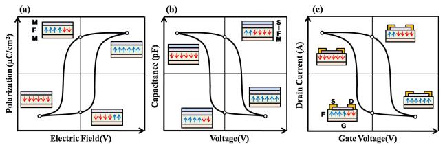
Ferroelectricity is a spontaneous electric polarization of a material that can be reversed by the application of an external electric field. A ferroelectric crystal thus exhibits a polarization–electric-field-hysteresis loop, analogous to the magnetization–magnetic-field-hysteresis loop exhibited by ferromagnetic materials [29, 30]. In addition, like magnetic materials, ferroelectric crystals can form domains, each with a unique polarization axis. The intercept of a hysteresis loop with polarization axis corresponds to the magnitude of the zero-field remanent polarization, Pr after saturation with a large electric field which typically determines the bistability margin of a memory device as shown in Figure 2a. The intercept with the applied electric field axis is called the coercive field Ec, the minimum value of the electric field necessary to reverse, or switch, the polarization state which is closely related to the operating voltage of the memory.
1.2 FERROELECTRIC MEMORY STRUCTURES
Early work for non-volatile memory based on ferroelectrics was done with thin films of ferroelectric perovskite oxides, which display bistable polarization at zero bias, designated as 0 and 1 states [31, 2]. Memory devices based on ferroelectric materials can be categorized into destructive and nondestructive mode. The destructive devices in ferroelectric memories include a basic memory element, ferroelectric capacitor device structure. Memory function in a capacitor is performed by electrically switching between the two states. In the destructive mode, loss of written data at one polarization state in a readout operation requires restoration by a rewriting cycle, which typically needs long access time and large memory cell area to accommodate the additional circuitry and at the same time limits operational life [32, 33]. On the other hand, the non-destructive devices are in the form of transistor types in which a ferroelectric thin layer is utilized as a gate insulator.
The initial ferroelectric memory test chip integrated with silicon CMOS consisted of only 256 bits; each bit contained two PbZr0.5Ti0.5O3 (PZT) capacitors that formed a nonvolatile shadow RAM for the accompanying six-transistor static random access memory cell (6T SRAM) [34]. Mass production of FRAM devices was realized in 1992 with the
IEEE Transactions on Dielectrics and Electrical Insulation Vol. 17, No. 4; August 2010 |
1137 |
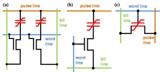
successful development of a 4 kbyte memory that utilized a high reliability two transistor, two-capacitor (2T2C) cell that was more area efficient than the early shadow RAM cells [35,36]. Since then, an exponential growth in FRAM capacity has been evidenced to a current maximum of 64 Mbytes with an exponential decrease in the integrated CMOS transistor gate length to 0.13 μm. Many other alternatives to PZT have been also extensively investigated including SrBi2Ta2O9 (SBT), (BiLa)4Ti3O12(BLT), (Bi,Nd)4Ti3O12(BNT), BaMgF4, Bi4 Ti3O12, and Pb5Ge3O11. The main motivation was to find an alternative ferroelectric material that could overcome the film degradation of the repeated ferroelectric polarization switching due to the chemical instability in the films and at the interfaces. The SBT-based products are currently limited to low memory capacity (less than 16 kbytes) for smartcard applications, although test chips with capacity as high as 4 Mbytes have been demonstrated [37]. In 2T2C devices as shown in Figure 1a, the ferroelectric capacitors are formed on top of a field oxide such that the capacitors are next to the accompanying transistors and each component of the cell occupies a uniquely defined area. This architecture is referred to as the capacitor-over-field-oxide (COFO) architecture, resulting in a relatively large 60F2 (F is the minimum feature size-the line-width and spacing of the electrodes) cell size.
When a switching charge pulse is detected from the capacitor in the device architecture of the one-transistor, one capacitor (1T1C) cell, the 1 state is stored in the cell capacitor as depicted in Figure 1b. On the other hand, when no switching charge is detected, the cell capacitor is in the 0 state. Due to the similarity of the device architecture of ferroelectric 1T1C cell to the current DRAM unit, several manufacturers have elaborately developed the arrays of 1T1C memories by scaling down their size in order to achieve both higher capacity and density. As part of the scaling effort to reduce cell size, the 1T1C FRAM cell has undergone an additional change in architecture where the ferroelectric capacitor was built on top of a plug that contacts an underlying access transistor. For the capacitor-on-plug (COP) architecture, a cell size of 18F2 was achieved [38, 39]. Three-dimensional ferroelectric capacitor which is essential for 6-8 F2 cell 1T1C FRAM, have been recently developed by introducing a new atomic layer deposition method for 3-D electrode and a novel MOCVD PZT deposition for 3D PZT[40].
A nondestructive readout of the nonvolatile ferroelectric capacitor polarization state has been proposed as an alternative way for overcoming the intrinsic limitations of 2T2C and 1T1C type memories to read/write endurance and memory unit cell size. In a destructive readout (DRO) scheme where the polarization state of the memory bit had to be switched in order to sense the stored memory state, the memory state was rewritten into the ferroelectric capacitor by resetting the polarization in reading process usually resulting in the reduced read and write switching endurance. Since many memory applications require more read accesses than writes, a nondestructive readout (NDRO) of the ferroelectric capacitor would necessarily increase endurance.
Figure 1. Ferroelectric memory cell structures (a)2T/2C (b)1T/1C (c)1T.
1.3 FERROELECTRIC FIELD EFFECT
TRANSISTOR MEMORY
Nonvolatile memory with a nondestructive readout capability and a smaller cell size has been extensively investigated in a memory structure based on one field-effect transistor (FET) (1T type memory) without additional capacitors as shown in Figure 1c[41, 42]. Ferroelectric thin films are required as gate dielectric to form a Ferroelectric Field-Effect Transistor (FeFET) device structure. The polarization state of the ferroelectric gate insulator set by the polarity of the writing gate voltage modulates the electrical conductance of the semi-conductor channel and thus distinguishes two logic states, the ON or OFF states of the channel current for memory function [43, 44]. Because spontaneous polarization directly controls channel conductance, there is neither the ferroelectric cell capacitance nor a high polarization required in the device operation, potentially leading to memory devices with high density as well as low-power consumption. In early demonstration of the 1T type FeFET memory, the inorganic ferroelectric films were integrated directly over the FET channel of a Si metal-oxide- semiconductor field-effect transistor (MOSFET) device [45]. The maximum voltage width of the hysteresis is defined as the memory window, one of the most important parameters of a FeFET. There are also various properties determining memory performance such as ON/OFF current ratio, switching time, and retention of the ON and OFF conductance of the channel and endurance.
Prior to full fabrication of a FeFET memory, the memory functions are usually examined in the simpler device structure of metal-ferroelectric-semiconductor (MFS) where capacitance of the device is controlled by the metal gate, giving rise to a capacitance memory hysteresis with read-write voltage margin. For the better memory performance, an insulating layer is frequently inserted between the ferroelectric layer and semi-conducting one to form a so-called MFIS memory unit. A prominent feature in a C-V curve of a MFIS memory unit is shown in Figure 2b. The measurement should be cautious to make sure that a hysteresis in a C-V curve arises unambiguously from ferroelectricity because uncompensated traps at the insulator/ semiconductor interface can also lead to hysteretic C-V curves. The hysteresis of the C-V curve reappears in the source-drain current versus gate voltage curve in a FeFET, as shown in Figure 2c.
1138 |
Y. J. Park et al.: Control of Thin Ferroelectric Polymer Films for Non-volatile Memory Applications |
Figure 2. Schematic plots of ferroelectric memory elements: (a) Polarization-voltage hysteresis of a MFM capacitor, (b) Capacitance-voltage hysteresis of a MFIS capacitor (c) Source-drain current vs. gate voltage hysteresis of a FeFET device.
1.3.1 INORGANIC FEFETS
The idea of the FeFET, presented in a patent in 1957 [46], was first realized by Moll and Tarui in 1963 [47], with triglycine sulphate (TGS) on a CdS substrate and implemented on silicon by Wu in 1974 [48]. A number of perovskite ferroelectric oxides, such as SrBi2Ta2O5 and Pb(Zr,Ti)O3, have been studied in the past. In an ideal FeFET the ferroelectric is in direct contact with the drain-source channel of the transistor. The ferroelectric is an active part of the transistor and the FeFET is a single device. The performance of the FeFET is therefore inextricably connected to its interface physics and the electronic properties of this interface. The interface is one of the most serious problems for the FeFET. The transistor properties such as threshold voltage, saturation voltage, or the C-V curve of the gate stack are strongly influenced by localized states (e.g., dangling bonds) and impurities at the interface. Interdiffusion between the ferroelectric and Si is another bottleneck for the FeFET.
Essential challenges for the FeFET are the improvement of the retention time and the suppression of serious parasitic effects such as the charge traps at the Si-ferroelectric interface. The problem of short retention times in FeFETs is believed to arise from the fact that the finite depolarization field due to the noncomplete charge compensation at the semiconductor side of the ferroelectric may lead to the formation of 180° domains or to current injection, both of which reduce the polarization in the ferroelectric film and consequently lead to information loss [49]. One possible solution in the case of a FeFET is to incorporate one insulating buffer layer between the Si and the ferroelectric [50, 51]. Several buffer layers, for example, SiO2, CeOx, and Si3N4, have been investigated. The recent works by using alternative gate oxides such as HfO2 or HfAlO show encouraging results. The retention time for the gate layer sequence Pt/SBT/HfO2 /Si was 30 days [50, 52]. Beside a low density of interface states the band offset between Si and the ferroelectric or the buffer needs to be sufficiently large to avoid electron injection during programming. The consequence is again a low retention time. Even more complex gate sequences have been investigated in the form of metal-ferroelectric-metal-insulator-silicon (MFMIS) structures [53]. The technological advantage here is that in this case
optimized MFM fabrication from FRAMs is used. To control the source-drain current of a field effect transistor a simulation showed that materials with a low Pr (~2 μC/cm2) are optimal. Since typical complex oxide ferroelectrics often exhibit more than ten times higher Pr, subloops are used to obtain sufficiently low Pr values and in addition to avoid electric breakdown of the buffer. Polymer ferroelectrics in general with relatively low Pr and high bandgap are, therefore, attractive for FeFET type non-volatile memory as shown next.
1.3.2 POLYMER FEFETS
Organic ferroelectric polymers are worth exploring as an alternative to perovskite ceramics. Polymers are chemically inert to Si and could be easily processed as thin films at relatively lower temperatures (< 200 °C) by solution-based techniques, which to a large extent addresses present concerns about stability of the Si-ferroelectric gate interface. Extensive studies of the crystalline structure and ferroelectric properties of the thin films of a number of polymers, polyvinylidene fluoride (PVDF) [54, 55], nylon-11 [56], and polyurea [57], ferroelectric liquid-crystalline [58] have been reported, which show considerable promise in this direction. Compared to most ferroelectric ceramic oxides, low dielectric constant (~13.8εo) of PVDF copolymer permits the use of SiO2 as a buffer layer (εSi =3.9 εo) without encountering large depolarization fields. Further, unlike ceramic ferroelectric structures, the integrity of ferroelectric polymer/SiO2 /Si interfaces is no longer an issue. In addition, the polymer ferroelectrics are conveniently combined with organic semiconductors such as pentacene, poly(3-hexylthiopene) (P3HT) and so on in the case of FeFET devices.
1.4 FERROELECTRIC POLYMERS
Many polymers show long-lived but transient polarization hysteresis arising from either charge injection or induced polarization. Either of the mechanisms provides polymer electrets defined as a kind of dielectric material exhibiting a quasi-permanent electrical charge. The consequent metastable piezoelectric and pyroelectric effects can last for hours, days or even years. Ferroelectric polymers on the other hand are
IEEE Transactions on Dielectrics and Electrical Insulation Vol. 17, No. 4; August 2010 |
1139 |
defined as polymers where the unit cell of the crystal is polar and the direction of polarization can be changed by the application of an electric field [26]. In the early 1970s it was discovered that poly(vinylidene fluoride) (PVDF) is ferroelectric which has a simple chemical structure with a repeat unit of –CH2-CF2-. Piezoelectric transducers made by solvent casting were soon commercially available, though it took a decade to establish that ferroelectricity was the origin of these effects in PVDF. PVDF is the most widely used ferroelectric polymer and is manufactured in large quantities for a wide variety of applications, ranging from protective coatings to ultrasound transducers.
Although PVDF shows clear repeatable polarization hysteresis, the origin of the hysteresis was also initially doubtful of whether it came from ferroelectric switching or electrets one. Direct evidence of ferroelectricity was first provided by X-ray diffraction studies [59] and further evidence that hysteresis was due to switching between opposing but equivalent polarization states was achieved by the synthesis and systematic study of the copolymers with trifluoroethylene (TrFE) [60] and tetrafluoroethylene (TeFE) [61]. The substitution of either TrFE or TeFE suppresses the ferroelectric–paraelectric phase-transition temperature below the melting point and thus allows a direct connection between the switching charge and the appearance of spontaneous polarization. Synthesis of PVDF and its copolymers has been standardized and is thoroughly described in the texts edited by Wang et al. [27] and Nalwa [28], and in several review articles [19,26–28].
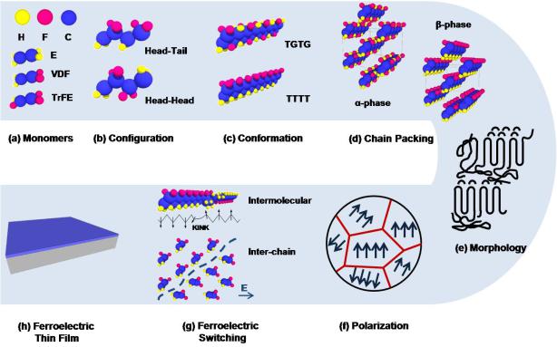
There are in general a number of structural requirements which meet to produce useful ferroelectric polymers including polar monomeric unit, head-to-tail configuration, all-trans conformation, polar chain packing, crystalline morphology, macroscopic polarity of the crystalline grains and reversible polar reorientation as shown in the schematic of Figure 3. The comprehensive description of PVDF and its copolymers with TrFE and TeFE is also given in the recent review based on the previous review articles [24,26-28]. We briefly summarize the characteristic molecular and microstructural features of the ferroelectric fluorocarbon polymers below.
In the monomeric unit of PVDF, the fluorine atoms with a van der Waals radius of 1.35 Å, similar to that of hydrogen (1.2 Å) form very polar bonds with carbon, giving rise to a
high dipole moment of 6.4×10− 30 Cm. The linear addition of
the repeating monomeric units leads to highly flexible main chain structure of PVDF with some stereochemical constraints [20]. In general, the PVDF chains have predominantly head- to-tail configuration, but other monomeric additions such as head-to-head and tail-to-tail defects can also occur to some extent (Figure 3b). These defects can subsequently affect the structural order and reduce the average dipole moment of the chain per repeat unit.
Three characteristic stereochemical conformations of PVDF chains have been known such as alternating trans (T) and gauche (G) (TGTG’), all-trans (TTTT), and TTTG as shown in Figure 3c. The packing of these polymer chains in the unit cell leads mainly to three polymorphic crystals corresponding
to α, β and γ, respectively. The non-polar α phase with the conformation of TGTG has been transformed into the other polar phases by various material processes such as thermal annealing, poling, compression, epitaxy and film stretching [60]. The optimal alignment of all the C-F dipoles is achieved by the chain conformation of consecutive all-trans conformation and thus the polar β phase with TTTT conformation is the most interesting polymorph for ferroelectric applications.
Alternatively in order to enhance the all-trans conformation, VDF is usually copolymerized with TrFE, which has three fluorine atoms per monomer. More steric hindrance by introducing TrFE units into the VDF chain which increases the unit cell size of the ferroelectric phase readily allows the formation of ferroelectric crystals with all-trans conformation. Replacement of the TrFE co-monomer by another type of monomer, such as vinylfluoride (VF) or tetrafluoroethylene (TeFE) in Figure 3a, also modifies the phase transition behavior markedly [28]. Copolymerization was also beneficial for improving the degree of crystallinity of a ferroelectric film. Over 90% crystallinity and 80% polarization with copolymers containing approximately 50-80% of VDF are easily obtained after simple thermal annealing even in the semi-crystalline polymer films containing both amorphous and crystalline microstructures schematically illustrated in Figure 3e while a PVDF film typically exhibits about 50% crystallinity and about 25% polarization at most requiring additional processes such as electrical poling and mechanical stretching for enhancing the crystallinity. Polarization switching is accomplished by applying a large electric field opposing the polarization (Figure 3f). The polarization reversal through successive 60º rotation of the dipoles under electric field has been proven by both experimental observations [62,63] and theoretical investigation [64] at the molecular level as schematically shown in Figure 3g.
1.5 THIN FILM FABRICATION OF
FERROELECTRIC POLYMERS
The electrical switching of ferroelectric polymers in general requires a relatively large coercive field of approximately the tens of MV/m. The low voltage operation of a memory device, therefore, critically requires the films as thin as one can. Although a variety of film preparation processes are potentially available with the ferroelectric polymers, there are mainly three techniques for thin film fabrication reported which include spin coating, vapor deposition and monolayer coating based on Langmuir Blodgett method. One of the major advantages of the ferroelectric polymers is their solution compatibility with common organic solvents and thus memory unit capacitors or transistors are easily fabricated by a simple spin-casting process. The ferroelectric polymer is first dissolved in an organic solvent at concentrations of a few weight percent. A variety of organic solvents have been used to dissolve PVDF and its copolymers for spin coating including dimethylformamide(DMF), acetone, methylethylketone(MEK), cyclohexanone and dimethyl sulfoxide (DMSO) and so on.
1140 |
Y. J. Park et al.: Control of Thin Ferroelectric Polymer Films for Non-volatile Memory Applications |
Figure 3. Hierarchical molecular and microstructures of thin films of ferroelectric PVDF and its copolymers with TrFE. (a) Monomeric units of VDF and TrFE, (b) Molecular configuration of the ferroelectric chains, (c) Various conformations of the ferroelectric polymer chains including TGTG, and TTTT, (d) Both non-polar and polar type crystalline structures, (e) Semi-crystalline nature of thin ferroelectric polymer films with crystalline lamellae and amorphous regions, (f) Polarization in multiple domains (g) Polarization switching of H-F dipoles in a ferroelectric polymer film based on 60° rotation model in which characteristic conformational kink initiates the dipole rotation, and (h) Ferroelectric film prepared by thin film fabrication techniques [24].
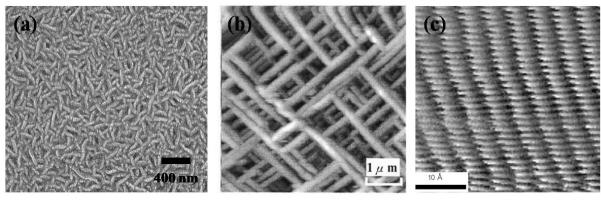
The solution is then formed into sheets or films by casting or spinning and the solvent evaporated, leaving a pliable solid sample that is typically polymorphous-an inhomogeneous mixture of amorphous and crystalline domains. Different from the semi-crystalline spherulitic morphology of PVDF and its copolymers with TrFE in 100 micron thick bulk samples, a thin film of in particular P(VDF-TrFE) with several hundred nanometers in thickness exhibits the characteristic needle-like crystalline domains. For instance, the ferroelectric domains which have typically 400 and 40 nm in length and width, respectively are well developed in a P(VDF-TrFE) film thermally annealed at a temperature below its melting point (~157 ºC) as shown in Figure 4a. It should be noted that the thin film preparation of the ferroelectric polymers sometimes needs special caution because they are very sensitive to water vapor as well as impurities in atmosphere.
Another notable innovation by a group at Kyoto University is the growth by epitaxial vapor deposition of crystalline VDF oligomers consisting of short iodine-terminated chains of VDF with the chemical formula CF3−[CH2 − CF2]17−I [65, 66]. The oligomer films are likely ferroelectric as they exhibit reversible switching. The oligomer films are promising alternatives to PVDF or its copolymers, but relatively little is known about their behavior. The oligomers are appealing for several reasons.
1)They have the same basic conformational structure as PVDF.
2)They are easily deposited by evaporation. 3) As monodispersed molecules, they crystallize more readily and should have fewer chain-folding defects and lamellar structures
than those that are prevalent in PVDF and its copolymers. In fact, the molecules grow epitaxially, influenced by single crystalline KCl surface [65-67]. The phase transformation from α phase to β phase was made by raising the substrate temperature from 50 to 80 ºC. A typical epitaxial morphology is shown of a vapor deposited VDF film on KCl surface in Figure 4b. The ferroelectric properties have been extensively investigated of the vacuum evaporated VDF thin films such as remanent polarization, coercive field and repeated polarization switching [68-70]. Thin PVDF films were also fabricated by a low-pressure chemical vapor polymerization process which involves polymerization of an isotropic vinylidene fluoride monomer condensate layer by cleavage of C double bonds using :CF2 initiators derived from hot-filament, thermochemical decomposition of the hexafluoropropylene oxide C3F6O. The method is beneficial because of its compatibility with submicrometer semiconductor device fabrication [71].
Two dimensional polymer ferroelectric films were successfully fabricated by horizontal (Schaefer) LangmuirBlodgett deposition which allowed more precise control of the film thickness by the number of the sequential layer deposition [2, 72]. The films show excellent crystalline and orientational order with the first order ferroelectric-paraelectric transition. All trans polymer conformational order was achieved in a quasi-hexagonal close packing with orthorhombic mm2 structure by the method as shown in Figure 4c and in turn attributed to the excellent ferroelectric properties even in a 1 nm thick film [72].
IEEE Transactions on Dielectrics and Electrical Insulation Vol. 17, No. 4; August 2010 |
1141 |
Figure 4. Microstructures of thin ferroelectric polymer film prepared by (a) spin coating and subsequent annealing at 135 ºC, (b) vacuum deposition of VDF oligomer on KCl substrate at 50 ºC [65], and (c) Langmuir-Blodgett deposition [72].
2 RECENT DEVELOPMENT IN POLYMER
FERROELECTRIC MEMORIES
2.1 METAL/FERROELECTRIC POLYMER/METAL
CAPACITOR
2.1.1 OPERATING VOLTAGE AND REMANENT
POLARIZATION
The recent studies have extensively focused on understanding the fundamental memory properties of metal/ferroelectric thin polymer film/metal (MFM) capacitors for the potential application of non-volatile 1T1C memory cells. The issues involved are operating voltage, remnant polarization, fatigue, thermal budget, imprint of a hysteresis curve, switching speed and data retention. The low operating voltage is one of the most important factors and thus makes our attention to the capacitors with the ferroelectric PVDF and its copolymers with TrFE films at least less than 200 nm in thickness due to their relatively high coercive field (Ec) of approximately 50 MV/m. A capacitor is operated at the lower voltage when the ferroelectric film becomes thinner and thinner. A MFM capacitor prepared with cyclohexanone solvent exhibited a fully saturated polarization hysteresis curve with the sweep voltage of ± 15 V due to the near defect-free film arising from the solvent [73]. The low voltage operating MFM capacitor with a P(VDF-TrFE) film at ±12 V was achieved by employing thin polypyrrole-poly(styrene sulfonate) acid film as interface layers between both bottom and top metal electrodes [74]. A recent work by Naber et al has also demonstrated a MFM capacitor with a P(VDF-TrFE) layer operating at 10 V when a PEDOT;PSS layer is inserted between bottom electrode and the ferroelectric polymer [75]. In spite of the concern of the rapid reduction of the degree of crystallinity at a film thinner than approximately 100 nm [76], the recent work by Ishiwara et al [77] has demonstrated a MFM capacitor with a 60 nm thick P(VDF-TrFE) film of approximately operating at the voltage as low as 5 V.
The remnant polarization value closely related to the degree of crystallinity of a film is mainly affected by thermal annealing in which degree of crystallinity tends to increase with the annealing temperature below the melting temperature of the film. Many experiments show that Pr of a P(VDF-TrFE) film becomes saturated by thermal annealing approximately at 120 °C, which guides a proper annealing temperature between its Curie and melting temperature. The absolute values of Pr obtained from MFM capacitors with the ferroelectric polymers range from 4 to 10 μC/cm2 [78,79]. VDF oligomer film evaporated on Pt surface gave rise to high Pr of 13±0.3 μC/cm2 due to extremely high crystallinity of the film [68]. The coercive field observed was, however, larger than those of P(VDFTrFE) which might be attributed to the steric hindrance arising from the presence of iodine atoms at the oligomer [68]. The mechanical bending resistance has been examined of a MFM capacitor containing a vacuum evaporated VDF film [69]. The work revealed that polarization hysteresis properties were not affected by one-dimensional bending with a radius of curvature down to 10 mm. The improvement of Pr was also reported in a MFM capacitor with a P(VDF-TrFE) film when a nucleating agent of diethyl phthalate was added due to the enhanced crystallinity of the film [80].
2.1.2 FATIGUE
The multiple polarization switching capability, i.e. fatigue of a ferroelectric polymer film has been extensively investigated in MFM capacitors in most cases with P(VDF-TrFE) films. An early work by Furukawa et al. observed the reduction of Pr as a sinusoidal electric field of amplitude decreased [81]. They employed the laser-induced current measurement technique and revealed that fatigue originated in the pinning of negative polarization charge to the electrodes on both interfaces probably due to annihilation of nucleation sites for polarization reversal. An interesting
1142 |
Y. J. Park et al.: Control of Thin Ferroelectric Polymer Films for Non-volatile Memory Applications |
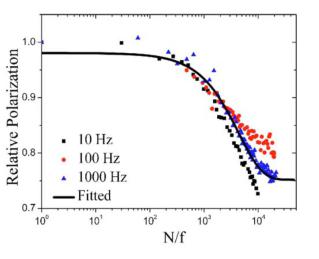
result is the frequency dependence of a metal/P(VDFTrFE)/metal capacitor in which the driving voltages with lower frequency and higher amplitude correspond to higher fatigue rates. Zhu et al have proposed a universal scaling behavior with N/f, where N is the number of switching cycles and f is the frequency in the fatigue behavior originating from the trapped charges, injected from electrodes into polymer films as shown in Figure 5 [82]. They also investigated the applied field dependent fatigue properties of the ferroelectric capacitors and showed that poor fatigue characteristics are observed for the higher electric field. The fatigue properties of a vacuum evaporated VDF thin film was also examined in which an oxide layer formed during the repeated polarization switching between the VDF film and Al electrode was strongly related to the properties of polarization reversal [70].
Fatigue properties of P(VDF-TrFE) films have been examined, depending upon the film preparation methods such as solution coating and mechanical stretching [83]. A solution cast sample exhibited the increase of the coercive field while a stretched sample displayed the decrease of the coercive field as the field cycles. The different fatigue behavior in two samples was understood by the change of the crystallinity, the orientation degree of the polymer chains, and electric dipoles as well as the interfacial layer effect. Fatigue properties of a MFM capacitor containing a P(VDFTrFE) layer was examined in particular with asymmetric electrodes [84]. A fatigued film with asymmetric top Au and bottom Al electrodes exhibited the occurrence of switching dual peaks and the jump of remanent polarization. To further understand electric fatigue of a P(VDF-TrFE) film with coexistence of crystalline phase and amorphous phase, Zhu et al [84] have recently employed a scanning probe microscope technique in which microscopic fatigue is determined by the attenuation of voltage-excited local vibration amplitudes at the crystalline inside and the boundaries between crystalline domains. They observed that the attenuation rate of vibration amplitude on crystalline domains is much slower than that at boundaries which indicates that the boundaries play a major role for fatigue decay of polarization due to the preferential trapping of space charges at the boundary regions.
An interlayer between electrode and P(VDF-TrFE) film turned out very effective to improve the fatigue resistance in MFM capacitors. Either a poly(3,4-ethylene dioxythiophene)- poly(styrene sulfonic) acid thin film [76] or a polypyrrolepoly(styrene sulfonate) acid film [75] inserted between metal and ferroelectric polymer not only prevents the reactions between P(VDF-TrFE) layer and Ti electrode during metallization process but also supplies the amount of charges needed for compensation of the ferroelectric dipoles to stabilize the domain during switching process, resulting in the improvement of fatigue property.
Figure 5. Normalized Pr as a function of logarithm of N/f, where f is the frequency of fatigue voltage. Fatigue was carried out by a bipolar triangular voltage with amplitude of 120 V and frequency of 10, 100, and 1000 Hz, respectively [82].
2.1.3 SWITCHING
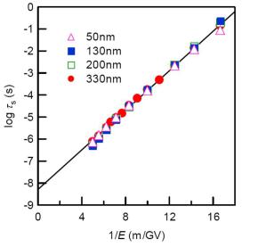
The switching characteristics of P(VDF-TrFE) films inserted top and bottom electrodes have been extensively investigated by Furukawa et al in which they observed that the switching time is independent of film thickness down to approximately 50 nm [86, 87]. Utilization of Au electrodes instead of Al ones turned out a key factor to improve the switching properties. The dependence of the switching time on the electric field was described by the exponential law of τs = τs∞ eEa/E where τs is switching time, τs∞ is a limited switching time, and Ea corresponds to an activation energy field [86]. The experimental results clearly exhibit the linear relationship between log τs and 1/E as shown in Figure 6. A limited switching time can be obtained from the extrapolation of the curve and is as low as 5 ns. For instance, with a 300 nm thick P(VDF-TrFE) film, as electric field increases, the switching time decreases from 100 ms at 60 MV/m to 500 ns at 200 MV/m with the reversed polarization remaining constant at approximately 8.5 μC/cm2.
The switching phenomena in ferroelectric polymers are assumed to be divided into three processes which include the interbond process, intermolecular expansion of chain rotations and interlamella expansion of polarization reversal [88]. The first interbond process involves 180 degree rotation of a single chain molecule which is again accomplished by the propagation of a kink along the chain direction [67]. In the next intermolecular expansion process, the chain rotation is associated with the ab plane of a crystalline lamella, based on the conventional nucleation and growth model characterized by the exponential increase of the switching rate with temperature and electric field. In the last process, the polarization reversal is propagated into interlamella regions of an aggregate of crystalline lamellae.
IEEE Transactions on Dielectrics and Electrical Insulation Vol. 17, No. 4; August 2010 |
1143 |
Figure 6. A plot of log τ s vs 1/E for thin PVDF/TrFE film obeying exponential law [86].
Since a kink of rotation is known to propagate along a 10 nm PVDF chains in a picosecond order which is much shorter than the switching time observed, now it is widely believed that the total switching process is controlled by the last two processes.
External switching involving the process of domain nucleation and growth has been identified as the dominant switching mechanism in ferroelectric thin polymer films. In the external switching the characteristic activation energy barrier of nucleation allows polarization switching at arbitrarily small fields and thus the switching does not have an intrinsic threshold coercive field. In addition, the apparent coercive field is a function of pulse duration or ac frequency in the typical AC measurement. As explained previously, thin films of PVDF and its copolymers show the coercive field up to approximately 50 MV/m while the coercive fields of most of ferroelectric materials, typically measured at 50-60 Hz, is in the range of 0.01-10 MV/m.
Intrinsic switching of ferroelectric P(VDF-TrFE) films prepared by Langmuir-Blodgett technique was first observed which involved the spontaneous and homogenous polarization reversal over the sample without the domain nucleation and growth [89]. Very high coercive field of approximately 500 MV/m remained constant with the film thickness ranging from 1 to 15 nm. In these thin films, extrinsic switching is suppressed due to the inhibition of nucleation arising from the limited nucleation volume. The intrinsic switching reported by Ducharme et al has been faced with some doubts about the misinterpretation of the experimental results produced in MFM capacitors with mainly Al electrodes. Several new and important data support the extrinsic switching mechanism and argue against intrinsic switching [90-92]. The thickness dependence of the LB films is not attributed to the intrinsic switching but due to the influence of electrode interfaces. Further investigation has been recently done to elucidate the switching behavior of a P(VDF-TrFE) capacitor by pulse train
measurement that involves the application of a train of unipolar on-off electric field pulses. The study found that polarization reversal was considerably delayed as pulse width became shorter than the conventional switching time, but it eventually completed even if pulse width was reduced to 0.2 μs [93]
2.1.4 IMPRINT
The asymmetric polarization switching frequently observed in a capacitor arises from the work function difference of the metal electrodes and the degree of asymmetry increases with the increasing work function difference. In addition, it is found that the polarization switching becomes much faster for a sample with high work function metals such as Ni [94]. The difference in the work functions of two electrodes produces an electric field in the ferroelectric polymer film and subsequently modifies the switching characteristics of the films. Asymmetric switching time was obtained for example by the potential difference between Al and Au electrode. Obviously the positive electric field yields the faster switching than the negative electric field as the consequence of the biasing electric field induced by the potential difference.
2.1.5 THERMAL BUDGET
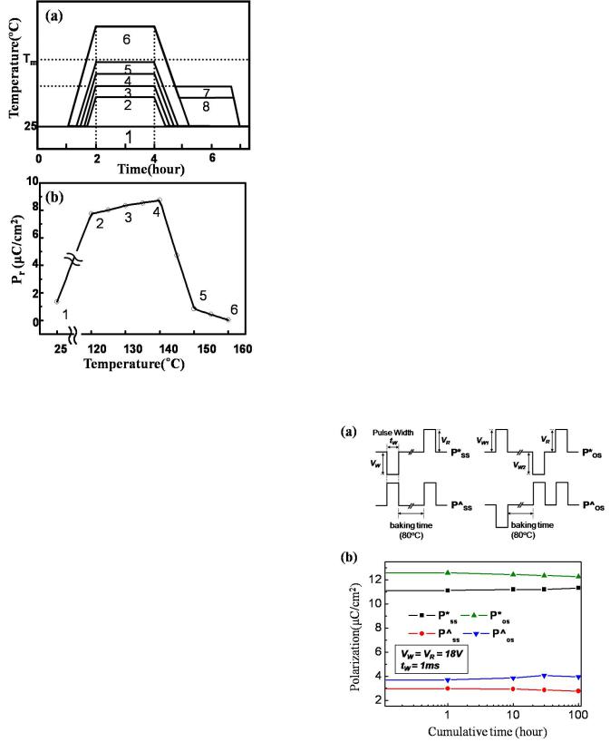
The proper adaptation of the polymer ferroelectrics into the current integrated process requires high temperature stability of the ferroelectric polymers well above their melting temperatures (Tm). In particular it is a critical issue for the fabrication and operation of a device whether or not the ferroelectric properties of a MFM capacitor are fully recovered from para to ferroelectric transition and vice and versa. For example, a capacitor should have the remanent polarization after the complete data erase similar to the value before thermal reset. Although PVDF and its copolymers with TrFE in general have fairly good thermal resistance up to approximately 250 °C due to their high degradation temperatures, the thermal hysteresis of ferroelectric properties turned out to strongly depend upon their melting and recrystallization. We have recently investigated the effect of thermal treatment of thin P(VDF-TrFE) films on ferroelectric properties [78]. The improved remanent polarization observed in the samples annealed at temperatures between Tc and Tm completely disappears when the samples are heated above Tm and re-crystallized through various pathways as shown in Figure 7 (the details of various pathways of 1~8 is explained in ref. [78]). Extinction of the remanent polarization of the melt-recrystallized samples arises from the modification of the molecular chain orientation upon recrystallization presumably due to the preferential crystal face interaction to the electrode surface. The molecular chain c-axis and polar b-axis are preferentially oriented perpendicular and parallel to the electrode surface, respectively, causing the effective electric field to the ferroelectric microdomains to be almost zero [78]. Our results suggest that a special treatment should be made to control the crystal orientation upon melting and recrystallization of the ferroelectric polymers.
1144 |
Y. J. Park et al.: Control of Thin Ferroelectric Polymer Films for Non-volatile Memory Applications |
Figure 7. (a) Thermal history routes for annealing treatments as a function of time. (b) Remanent polarization measured at room temperature from MFM capacitors thermally annealed at various temperatures indicated [78].
2.1.6 RETENTION
Data retention, defined by the ability to store the written state for certain period of time, is essential for successful realization of ferroelectric polymer memory devices. Considering that a number of studies have been done of the retention characteristics in inorganic ferroelectric thin film capacitor structure including mechanisms for retention loss [95], comparative polarization retention in metal oxide electrodes etc [96], studies were seldom performed to characterize polarization retention loss in P(VDF-TrFE) thin film capacitors. We have monitored the retention loss of Al/ferroelectric P(VDF-TrFE)/Al capacitors with four kinds of pulse trains shown in the schematic of Figure 8a in order to characterize both switched and non-switched polarization for each same and opposite state mode. After a period during which the sample was held at the state preset by an initial writing pulse, the second pulse switches the sample to the other state and measures the switched polarization (P*). When the second pulse was applied with the same direction of a preset written pulse, we can measure the nonswitched polarization (P^). Each P* and P^ is characterized by two different test modes: same and opposite state. There are, therefore, four different sequences of the programmed pulses to characterize the retention properties. Left two pulses were used to measure the same-state retention and the other ones were relevant to the opposite-state retention in Figure 8a. The same-state
retention tests evaluate the retaining ability of a previously given logic state. The reading pulse applied at room temperature measures either switched (P*ss) or nonswitched (P^ss) retained polarization, dependent upon the initial writing voltage for the same state retention test as illustrated by the pulse trains in the left two schemes of Figure 8a. On the other hand, the opposite-state retention test measures how much a given amount of polarization is maintained after an additional writing voltage is given, opposite to a previous input stored for a long time. A device with an input voltage VW1 which determines a written state at the beginning is baked for a certain time before which the second writing pulses of VW2 is delivered to induce the logic state opposite to VW1. Final reading pulses (VR) were subsequently applied to measure the switched (P*os) and non-switched (P^os) polarization. Almost complete retention of the initial remanent polarization in the same and opposite mode at 80 °C over 100 h was observed at ±18 V and 1 ms in writing pulse amplitude and time width, respectively as evidenced in Figure 8b. The retention was significantly deteriorated when both writing pulse amplitude and time width decrease. Non-switching retention in the opposite state mode turned out one of the most important properties for realizing a non-volatile ferroelectric polymer memory capacitor [97]. The detailed characteristics of MFM elements recently reported with thin ferroelectric polymer films are summarized in Table 1.
Figure 8. (a) Four sequences of programmed test pulses for the characterization of retention properties, switched (P*) and nonswitched (P^) polarization of the same- (SS) and the opposite-state (OS) retention. (b) The time dependent variations of switching polarization values (P*ss and P*os) and nonswitching ones (P^ss and P^os) in Au/P(VDF-TrFE)(150nm)/Al capacitors, with the pulse
width and amplitude of 1 ms, ±18V, respectively [97].