

172 Radio Engineering for Wireless Communication and Sensor Applications
of the semiconductor devices over the electron tubes are their small size, low weight, low supply voltage, and long lifetime.
Circuits based on semiconductor devices may be either active or passive. A circuit is said to be active if it generates RF power from dc power (oscillator) or it amplifies an RF signal (amplifier). In a broader sense, we can consider some other circuits as active: A mixer, frequency multiplier, detector, modulator, and demodulator are all active because they convert power from one frequency to another. However, not all circuits containing semiconductor devices, that is, diodes and transistors, are active. They are also used to realize switches, attenuators, phase shifters, and loads needed in impedance matching (e.g., active matching in MMICs). Figure 8.1 presents standardized drawing symbols of some circuits based on semiconductor components.
8.2 Important Semiconductor Devices
Semiconductor technology has advanced rapidly during the last decades. Several types of diodes and transistors are available for RF and microwave applications. The fastest transistors are usable at frequencies over 200 GHz and the fastest diodes at frequencies over 3 THz. The structures and operation principles of the most important diodes and transistors are treated in this section. A more detailed analysis of their physics can be found in the literature [1–3].
8.2.1 Diodes
The simplest semiconductor diode is the p-n diode shown in Figure 8.2(a). It is based on the interface of p- and n -type semiconductors. The semiconductor is most often silicon (Si), germanium (Ge), or gallium arsenide (GaAs).
Figure 8.1 Drawing symbols for circuits based on semiconductor devices.
|
|
|
|
|
Circuits Based on Semiconductor Devices |
173 |
||||||||||||||
|
|
|
|
|
|
|
|
|
|
|
|
|
|
|
|
|
|
|
|
|
|
|
|
|
|
|
|
|
|
|
|
|
|
|
|
|
|
|
|
|
|
|
|
|
|
|
|
|
|
|
|
|
|
|
|
|
|
|
|
|
|
|
|
|
|
|
|
|
|
|
|
|
|
|
|
|
|
|
|
|
|
|
|
|
|
|
|
|
|
|
|
|
|
|
|
|
|
|
|
|
|
|
|
|
|
|
|
|
|
|
|
|
|
|
|
|
|
|
|
|
|
|
|
|
|
|
|
|
|
|
|
|
|
|
|
|
|
|
|
|
|
|
|
|
|
|
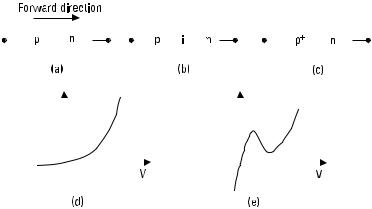
Figure 8.2 (a) p-n diode; (b) p-i-n diode; (c) tunnel diode; (d) I–V characteristic of a p-n diode; and (e) I–V characteristic of a tunnel diode.
In a p-n junction, current is carried by minority carriers, that is, by holes injected into the n -side and by electrons injected into the p -side. In the forward direction the current increases exponentially as the applied voltage increases as shown in Figure 8.2(d). In the reverse direction only a small saturation current flows. Because of the large diffusion capacitance due to the minority carriers, the use of the p-n diode is limited to low frequencies, a few hundred MHz at maximum. The p-n diode is used in rectifiers and detectors.
A reverse-biased p-n diode is used as a varactor, that is, as a voltagedependent capacitor. It is used as an electrically controlled tuning element, but also in modulators, switches, frequency multipliers, and parametric amplifiers.
When an intrinsic (undoped) semiconductor layer is added in between the p - and n -regions, a p-i-n diode, shown in Figure 8.2(b), is formed. The intrinsic semiconductor layer decreases considerably the junction capacitance, and therefore the p-i-n diode is well suited to many microwave circuits. It is used in rectifiers, modulators, attenuators, switches, phase shifters, and limiters.
A tunnel diode is a p-n junction with both sides very heavily doped, as shown in Figure 8.2(c). The depletion region becomes very narrow and therefore allows a remarkable tunneling current at a low forward bias. Its I–V curve has a negative differential resistance region, as shown in Figure 8.2(e). The tunnel diode is well suited to oscillators and detectors.
In a forward-biased p-i-n diode, carriers are accumulated in the i -region and therefore the diffusion capacitance is high. However, this accumulated
174 Radio Engineering for Wireless Communication and Sensor Applications
charge is suddenly released when the bias is reversed: A short reverse current pulse is generated. This extremely nonlinear behavior is utilized in the steprecovery diode, which is used in frequency multipliers and comb generators for producing frequencies of high harmonic number [4].
The most important diode suitable for microwave detectors, mixers, and frequency multipliers is the Schottky diode. It is an interface between an n -type semiconductor (Si or GaAs) and a metal (Au, Pt, or Ti). Minority carriers (holes) play a negligible role, and therefore a Schottky diode is very fast, that is, it can switch from a conducting state to a nonconducting state very quickly. GaAs-Schottky diodes are used up to 3 THz.
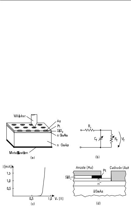
A Schottky diode can be contacted and packaged in many ways. In Figure 8.3(a) an unpackaged, whisker-contacted Schottky diode is shown. There are many small anodes on the surface of the GaAs chip; one of them is contacted to the embedding circuit with a sharp wire, a whisker. The planar Schottky diode shown in Figure 8.3(d) can be used as a flip-chip component on a microstrip circuit, it can be encapsulated as a beam-lead diode, or it can be integrated monolithically.
Figure 8.3(b) shows an equivalent circuit of a Schottky diode. It consists of a voltage-dependent junction resistance R j , a voltage-dependent junction
Figure 8.3 Schottky diode: (a) GaAs diode chip; (b) equivalent circuit; (c) I–V characteristic; and (d) planar diode.
Circuits Based on Semiconductor Devices |
175 |
capacitance Cj , and a series resistance R s . When the Schottky diode is connected to a circuit, it always has a series inductance as well and may have an extra fringing capacitance which both decrease its performance.
The I–V characteristic shown in Figure 8.3(c) is exponential as
I (Vj ) = Is (e aVj − 1) |
(8.1) |
|||||
a = |
q |
= |
1 |
|
(8.2) |
|
hkT |
V 0 |
|||||
|
|
|
||||
where Is is the saturation current, q is the magnitude of the electron charge, h is the ideality factor, k is Boltzmann’s constant, and T is the absolute temperature. The ideality factor of a good diode at room temperature is slightly above unity. The junction differential resistance is obtained from the I–V characteristic as
R j = |
|
dI |
−1 |
= |
1 |
≈ |
V 0 |
(8.3) |
||
|
|
|
|
|
|
|||||
SdVj |
D |
a (I + Is ) |
I |
|||||||
|
|
|
|
|||||||
The junction capacitance is also voltage dependent and behaves as
Cj (Vj ) = |
|
Cj 0 |
(8.4) |
|
− Vj /fi )g |
||
(1 |
|
||
where Cj 0 is the junction capacitance at zero voltage, fi is the contact potential, and g is a constant depending on the doping profile of the epitaxial layer. For a GaAs–Pt junction fi is about 1 V. If the doping profile is abrupt, we have g = 0.5.
When a Schottky diode is used as a detector or mixer, its figure of merit is the cutoff frequency:
f c = |
1 |
(8.5) |
|
||
|
2pR s Cj |
|
The series resistance R s is mainly due to the low mobility of electrons in the undepleted epitaxial layer; it is also called the spreading resistance. At the cutoff frequency, one half of the voltage applied over the diode is over the series resistance. The cutoff frequency should be much higher than
176 Radio Engineering for Wireless Communication and Sensor Applications
the operating frequency ( f c ≥ 10f ). A Schottky varactor has basically the same structure and equivalent circuit as the mixer diode; its behavior is based on the voltage-dependent capacitance, and it is used in frequency multipliers.
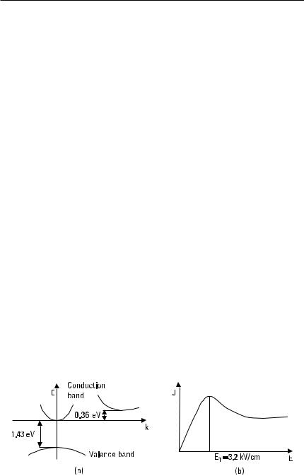
In oscillators a device with negative resistance is needed. Besides the tunnel diode, a Gunn diode and an impact ionization avalanche transit time
(IMPATT) diode have a negative resistance region in their I–V characteristics. The Gunn diode, named for its inventor but also called a transferred electron device (TED), is not a rectifying diode but rather a piece of n -type bulk semiconductor. Its negative resistance is based on the properties of the energy band structure of the III–V semiconductors, such as GaAs or indium phosphide (InP). In these semiconductors, electrons with sufficiently high energy transfer from the main valley of the conduction band to a satellite valley, where their effective mass is higher and their mobility lower than in the main valley. Therefore, above a given electric field E = ET the average drift velocity of electrons decreases while E increases; in other words, the differential resistance of the semiconductor is negative. Figure 8.4 illustrates the energy band structure and current density versus electric field in n -type
GaAs.
Figure 8.5(a) presents different structures of the IMPATT diode. When a sufficiently high reverse voltage is applied over the diode, an avalanche breakdown (electron-hole pairs are rapidly and increasingly created) occurs in the p-n interface, where the electric field is highest. For example, in a p +-n-n + structure the holes go directly to the p +-region but the electrons drift through the n -region (so-called drift region) to the n +-contact. When an alternating voltage is applied over the diode in addition to the dc bias, the phase of the generated electron pulse is 90° behind the voltage phase. With a proper thickness of the n -layer, an additional phase shift of 90° occurs, due to the drift time. Then the current and voltage of the diode are
Figure 8.4 (a) Energy band structure and (b) current density versus electric field in n -type GaAs.