

78 Radio Engineering for Wireless Communication and Sensor Applications
radius of which is equal to the absolute value of the load reflection coefficient. If the movement is toward the load, the direction on the Smith chart is counterclockwise. If the movement is away from the load, that is, toward the generator, the direction is clockwise. The impedance of the load, z L = 0.5 + j 0.5, seen through a line of 0.1lg long, is obtained by moving from point A clockwise 360°/5 = 72° to point B, where the impedance is z B = 1.42 + j 1.11.
One of the great features of the Smith chart is that the admittance y L corresponding to the impedance z L is obtained as the mirror image A′ of point A. When z L = 0.5 + j 0.5, we can read from the Smith chart that y L = 1.0 − j 1.0. This can be easily checked using the definition of admittance
1 |
= |
Z 0 |
= g + jb |
|
|
y (−l ) = |
|
|
(4.25) |
||
z (−l ) |
Z in (−l ) |
||||
4.3 Matching Methods
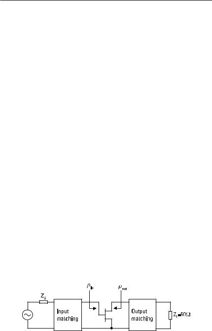
The purpose of matching is to eliminate the wave reflected from a load. From the matching point of view, a load may be not only a circuit or device into which the power is absorbed from the line, but also a generator feeding the line. This is why we have to consider cautiously the directions ‘‘toward generator—clockwise’’ and ‘‘toward load—counterclockwise’’ on the Smith chart. In most cases we measure the reflection coefficient of the ‘‘load’’ first. In the measurement we use an auxiliary generator, and accordingly we can always use the direction ‘‘clockwise—toward generator’’ when designing a matching circuit. Figure 4.6 illustrates this in the case of an amplifier with both an input and output matching circuit in order to maximize gain. When designing the input matching circuit, we measure first the transistor reflection coefficient, r in , from the input side, but when designing the output matching circuit we measure the reflection coefficient, rout , from the output side.
Figure 4.6 A transistor amplifier with both input and output matching, illustrating the direction of measurement of the reflection coefficients.
Impedance Matching |
79 |
Note that impedance tuners are needed in place of matching circuits to optimize the transistor performance before and during measurement. In the case of a bilateral transistor, r in depends on the output load impedance and rout depends on the input load impedance. Therefore, some iteration is needed to find the reflection coefficients providing the maximum gain. After these measurements, in both cases, we use the Smith chart in a clockwise manner when designing the matching circuits.
Usually the load is matched to the line with a matching circuit in front of the load. The matching circuit contains reactive elements such as inductors (coils), capacitors, transformers, tuning stubs, or special elements such as a tuning screw or an iris in a metal waveguide. The reactive elements represent discontinuities that cause reflections, which cancel the reflection from the load, so that ideally all power is absorbed into the load although there are multiple reflections between the load and the matching circuit (see Section 4.3.3). In case of a quarter-wave transformer these discontinuities are the abrupt changes in the characteristic impedance of the line. In some cases the load is matched resistively, but then the reflected wave is absorbed into the matching circuit and therefore lost.
Furthermore, in some cases the load impedance can be tuned actively. For example, the impedance of a diode detector depends on the diode bias current. By introducing a proper bias current, the matching of the detector can be optimized.
In Section 4.3 we assume that the load impedance will be matched to the real impedance of the line feeding the load. Generally, matching is realized between circuits having complex impedances—for example, between a source with an output impedance Z S and a load with an input impedance Z in . Then conjugate matching
Z in = Z S* |
(4.26) |
results in maximum power transfer to the load for a fixed source impedance. In fact, in the following we realize the same because the matching circuit transforms the real line impedance to the complex conjugate of the load impedance.
4.3.1 Matching with Lumped Reactive Elements
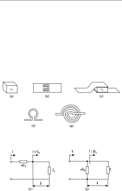
In the megahertz range, a coil may perform as an ideal inductance and a capacitor as an ideal capacitance. In the microwave region, coils and capacitors may still be useful elements for realizing reactive matching circuits, but care
80 Radio Engineering for Wireless Communication and Sensor Applications
must be taken with the size of these elements. The size of the lumped element must be much smaller than a wavelength. In hybrid integrated circuits, chip capacitors or interdigital gap capacitors and wire coils are successfully used at least to several gigahertz, and in monolithic integrated circuits metal– insulator–metal (MIM) capacitors as well as loop and spiral inductors are used successfully at millimeter wavelengths. However, parasitic elements of such capacitors and inductors must also be taken into account in the circuit design, meaning that a careful modeling of these elements is necessary. Figure 4.7 illustrates some lumped elements used in integrated circuits.
Matching with a lumped reactive element is realized by placing a single element at a proper distance from the load in series or in parallel as shown in Figure 4.8. It is possible to move from any load impedance z L toward the generator such a distance l 1 < l g /2, so that the load is seen as an impedance 1 + jx 0 . If we add at this point a series reactance of −x 0 , the
Figure 4.7 Reactive lumped elements for integrated circuits: (a) chip capacitor; (b) interdigital gap capacitor; (c) metal–insulator–metal capacitor; (d) loop inductor; and (e) spiral inductor (with an airbridge).
Figure 4.8 Matching with a single reactive element placed at a proper distance from the load: (a) with a series element; and (b) with a shunt element.
Impedance Matching |
81 |
input impedance is 1 + jx 0 − jx 0 = 1, and the load is matched to the line; see Figure 4.8(a). On the other hand, from any load admittance it is possible to move toward the generator a distance l 2 < l g /2, so that the load admittance is seen as 1 + jb 0 . By adding in this point a shunt susceptance −b 0 , we get a match, as in Figure 4.8(b).
Example 4.1
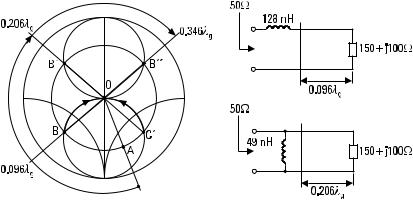
Match a load impedance of Z L = R L + jX L = (150 + j 100)V to Z 0 = 50V at 100 MHz according to Figure 4.8.
Solution
Let us first place the normalized load impedance z L = Z L /Z 0 = 3 + j 2 on the Smith chart in Figure 4.9; we are at point A. If we then move along a circle (radius OA) clockwise on the Smith chart (corresponding to moving along a lossless 50-V line away from the load), we first come to the unity circle after 0.096lg at point B, where the impedance is 1 − j 1.62. By adding a series inductance with a normalized reactance of x = +1.62 (L = xZ 0 /v = 128 nH) in this point, we match the load. Another possibility is to move further away (a distance of 0.206l g from load) to point B′, which is on the mirror image circle of circle r = 1. The corresponding admittance at point C′ is 1 + j 1.62. By adding a shunt inductance with susceptance of b = −1.62 (L = −Z 0 /(v b ) = 49 nH) at this point we also match the load. A further possibility is to move to point B″ (distance from load 0.346l g ) and add a shunt capacitance with susceptance of b = +1.62 (C = b /(vZ 0 )
Figure 4.9 Matching the load impedance of Z L = R L + jX L = (150 + j 100)V to Z 0 = 50V using a single lumped reactive element.
82 Radio Engineering for Wireless Communication and Sensor Applications
= 52 pF). However, the widest matching bandwidth is obtained when the reactive (susceptive) element is placed as close to the load as possible.
Another possibility in realizing a reactive match is to use an LC (or LL or CC ) circuit in front of the load, as shown in Figure 4.10. The series or shunt element next to the load now replaces the line section needed above, and the matching circuit is more compact.
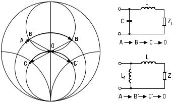
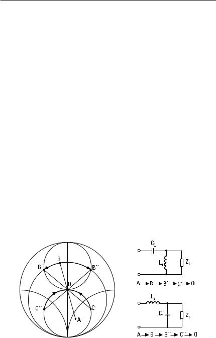
If z L = r L + jx L is inside the 1 + jx circle, there are two distinct possibilities to match the load with two reactive elements: first either a capacitor or an inductor in parallel to the load and then in series an inductor or a capacitor, respectively, toward the line. If z L = r L + jx L is inside the mirror image circle of the 1 + jx circle, there are again two distinct possibilities: first either an inductor or a capacitor in series with the load and then a
Figure 4.10 Matching with two reactive elements: Depending on the value of the load impedance z L = r L + jx L , the Smith chart is divided into four regions, each of which leads to different possibilities in matching with two reactive elements.
Impedance Matching |
83 |
shunting capacitor or inductor, respectively, toward the line. If the load impedance is outside of both of the regions, in the vertically or horizontally shaded area of the Smith chart in Figure 4.10, there are more matching possibilities. If the load impedance z L = r L + jx L is in the vertically shaded area, that is, if z L is capacitive, there are four distinct possibilities to construct the matching circuit with two reactive elements, but we must start with an inductor next to the load. This inductor may be either in series or in parallel; the other component (respectively in parallel or in series) may be an inductor or a capacitor. Similarly, when z L is in the horizontally shaded region— when the load impedance is inductive—there are again four different possibilities, but now we must start with a capacitor next to the load. Again, this capacitor may be either in series or in parallel; the other component (respectively in parallel or in series) may be an inductor or a capacitor. Let us study these in more detail through some examples, which also serve the reader for getting more confidence in using the Smith chart.
Example 4.2
Match a load impedance of Z L = R L + jX L = (20 − j 30)V to Z 0 = 50V at 100 MHz starting with a series inductor next to the load.
Solution
Let us first mark the normalized impedance z L = Z L /Z 0 = 0.4 − j 0.6 on the Smith chart as shown in Figure 4.11; we are at point A. If we add at this point a series reactance of x = 1.09, we get to the mirror image circle of the circle r = 1 to point B, where the impedance is 0.4 + j 0.49. The
Figure 4.11 Matching of a load Z L = R L + jX L = (20 − j 30)V to Z 0 = 50V using lumped reactive elements.
84 Radio Engineering for Wireless Communication and Sensor Applications
corresponding admittance is 1.0 − j 1.22 (point C), so that by adding a parallel susceptance of b = 1.22, we match the load. The inductance corresponding to the normalized series reactance x is L = xZ 0 /v, and the capacitance corresponding to the normalized parallel susceptance is C = b /(v Z 0 ). The component values at 100 MHz are L = 87 nH and C = 39 pF. Another possibility is first to add a small series reactance of x = 0.11 to get to point B′ where the impedance is 0.4 − j 0.49. Then the corresponding admittance is 1.0 + j 1.22 (point C′). After adding a parallel susceptance of b = −1.22, we also have obtained a match. Now both of the reactive components are inductances; the series component is L 1 = Z 0 x /v = 8.8 nH and the parallel component is L 2 = −Z 0 /(bv ) = 65 nH. (Note: This load impedance can also be matched starting with a shunt inductance next to the load; in order to realize this, start from the load admittance.)
Example 4.3
Match a load impedance of Z L = R L + jX L = (150 + j 100)V to Z 0 = 50V at 100 MHz with two reactive elements.
Solution
Let us first mark the normalized impedance z L = Z L /Z 0 = 3 + j 2 on the Smith chart as shown in Figure 4.12; we are at point A. We first transform to the corresponding admittance, y L = 0.23 − j 0.15. From there we move along circle g = 0.23 to the mirror image circle of g = 1 either to point B′ or point B″. Moving to B′ corresponds to adding a shunt susceptance of b = −0.26 (i.e., L 1 = −Z 0 /(bv) = 306 nH), and moving to B″ corresponds
Figure 4.12 Matching of a load Z L = R L + jX L = (150 + j 100)V to Z 0 = 50V using lumped reactive elements.
Impedance Matching |
85 |
to adding a shunt susceptance of b = 0.56 (i.e., C1 = b /(vZ 0 ) = 18 pF). Then we transform back to the impedance and get to either point C′ or C″, respectively. In order to get to the center of the Smith chart, we now have to add a series component. In the case of point C′ we add a series capacitor with a reactance of x = −1.8 (C2 = −1/(Z 0 xv ) = 18 pF), and in the case of point C″ we add a series inductor with a reactance of 1.8 (L 2 = xZ 0 /v = 143 nH).
Example 4.4
Match a load impedance of Z L = R L + jX L = (15 − j 15)V to Z 0 = 50V at 100 MHz with two lumped reactive elements.
Solution
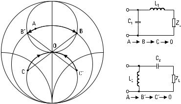
Let us first mark the normalized impedance z L = Z L /Z 0 = 0.3 − j 0.3 on the Smith chart as shown in Figure 4.13; we are at point A. If we now add a series reactance of x = 0.758, we move along the circle r = 0.3 and get to the mirror image circle of the circle r = 1 to point B, where the impedance is 0.3 + j 0.458. The corresponding admittance is 1.0 − j 1.528 (point C), so that by adding a parallel susceptance of b = 1.528 we match the load. The inductance corresponding to the normalized series reactance x is L 1 = xZ 0 /v = 60 nH, and the capacitance corresponding to the normalized parallel susceptance is C1 = b /(v Z 0 ) = 49 pF at 100 MHz. Another possibility is to add first a series reactance of x = −0.158 to get to point B′ where the impedance is 0.3 − j 0.458. Then the corresponding admittance
Figure 4.13 Matching of a load Z L = R L + jX L = (15 − j 15)V to Z 0 = 50V using lumped reactive elements.

86 Radio Engineering for Wireless Communication and Sensor Applications
is 1.0 + j 1.528 (point C′). After adding a parallel susceptance of −1.528, we have obtained a match. Now the component values are for the series capacitance C2 = −1/(Z 0 xv) = 201 pF and for the parallel inductance L 2 = −Z 0 /(bv) = 52 nH.
4.3.2 Matching with Tuning Stubs (with Short Sections of Line)
In the microwave region, the inductors and capacitors do not represent ideal inductances and capacitances but often behave as resonant circuits. At such high frequencies the desired reactance may often be more easily realizable by using a tuning stub, which is a short section of a line terminated with either a short circuit or an open circuit. As we can easily calculate using (4.12), a short-circuited tuning stub is inductive when its length is from 0 to lg /4 and capacitive when its length is from l g /4 to l g /2. An opencircuited tuning stub is capacitive when its length is from 0 to lg /4 and inductive when its length is from lg /4 to l g /2. Depending on the line type used, there may be only one choice: In a metal waveguide only a shortcircuited stub is possible because an open end acts as an antenna. On the other hand, in microstrip circuits a short circuit is difficult to realize and therefore open-circuited stubs are used.
Matching with one tuning stub is realized according to Figure 4.8. In theory, we can use either a series stub or a parallel stub. In practice the choice is more limited. For example, in a microstrip circuit only a parallel stub is possible.
If the characteristic impedance of the tuning stub is the same as that of the line to which the load is to be matched, the length of a short-circuited stub is obtained from the following [see also (4.12)]
j tan bl = −jx 0 = |
1 |
|
(4.27) |
|
−jb 0 |
||||
|
|
|||
Accordingly, the length of an open-circuited stub is obtained from
1 |
= −jx 0 = |
1 |
|
(4.28) |
|
j tan bl |
−jb 0 |
||||
|
|
||||
The characteristic impedance of the stub may also differ from that of the line; then the proper length is calculated using (4.12). Since the impedance
Impedance Matching |
87 |
of a stub is periodic with a period of l g /2, the stub length can also be l + nlg /2, but a short stub is preferred because it provides a wider matching bandwidth.
Example 4.5
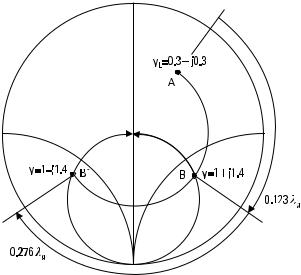
Match the normalized admittance of y L = 0.3 + j 0.3 to a 50-V line using a short-circuited tuning stub.
Solution
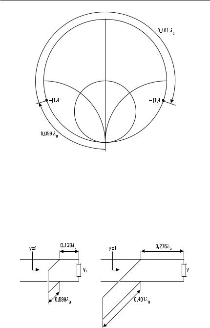
Figures 4.14 and 4.15 show how this problem is solved on the Smith chart. First we place the normalized admittance on the Smith chart, point A. Then we move along a circle (along a 50-V line) a distance of 0.123lg and come to the unity circle g = 1 to point B, where the admittance is 1 + j 1.4. If we now add at this point a parallel susceptance of −1.4, we obtain a match. Another possibility is to move along the 50-V line to point B′, where the admittance is 1 − j 1.4, and add at this point a parallel susceptance of +j 1.4 in order to get a match. The required length of the parallel stub is either obtained from (4.27) or by using the Smith chart. Figure 4.15 shows how the length of a short-circuited stub with a normalized admittance of −j 1.4 is obtained. We start from y = ∞ and move along the outer circle of the
Figure 4.14 Matching of a load with a shunt susceptance according to Figure 4.8(b) presented on the Smith chart.
88 Radio Engineering for Wireless Communication and Sensor Applications
Figure 4.15 Using the Smith chart to obtain the lengths of short-circuited tuning stubs corresponding to normalized admittances of −j 1.4 and +j 1.4.
Smith chart to the point where the normalized admittance is −j 1.4: The length l = 0.099l g can be read from the Smith chart. Accordingly, the admittance +j 1.4 can be realized with a short-circuited stub of length l = 0.401l g , as also shown in Figure 4.15. The obtained matching circuits are presented in Figure 4.16.
Figure 4.16 Tuning-stub matching of a load with a normalized admittance of y L = 0.3 + j 0.3.
Impedance Matching |
89 |
The above matching with a single tuning stub is simple but requires placing the stub in a new position when the frequency is changed, even if the stub length is adjustable. The tuning stubs can be placed in a fixed position when two or three stubs are used [3]. The remaining task is to find correct lengths of the stubs. Two tuning stubs allow matching of almost all possible load impedances. In practice, a limiting factor is the attenuation in the line; it limits the range of the obtainable stub susceptances. A wide matching bandwidth also requires that the distance between the stubs be close to either 0 or lg /2. In practice the tuning stubs are placed at a distance of l g /8 or 3lg /8 from each other. For measurement setups, tuners are available with three adjustable stubs. Such a tuner can match any load impedance to the line.
4.3.3 Quarter-Wave Transformer
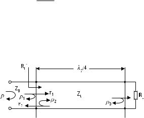
Let us consider the situation presented in Figure 4.17. A real load impedance R L must be matched into a line with a characteristic impedance of Z 0 . Matching is realized by using a line section of length lg /4 and characteristic impedance Z t . Because tan ( bl g /4) = ∞, we obtain from (4.12) that the impedance loading the original line is
RL′ = |
Z t2 |
|
|
(4.29) |
|
|
||
|
R L |
|
If we choose Z t = √Z 0 R L , the load is matched to the line. The quarter- wavelength-long line section acts as a transformer, with a number-of-turns ratio equal to √Z 0 /R L . If the load impedance is not real, we use a line section with a proper length and characteristic impedance between the load and the transformer so that the load impedance seen through this section is real.
Figure 4.17 Quarter-wave transformer.
90 Radio Engineering for Wireless Communication and Sensor Applications
Example 4.6
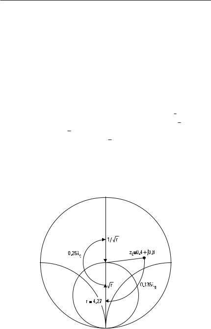
Match a load impedance of Z L = (20 + j 40)V to a line with Z 0 = 50V using a quarter-wave transformer.
Solution
Figure 4.18 shows, on the Smith chart, how the problem is solved. First we need to make the load impedance real: We place a line section having a
characteristic impedance of Z 0 between the load and the transformer. The load impedance normalized to Z 0 is z L = 0.4 + j 0.8. We need a line section of 0.135lg to make the load impedance real. When we move from z L = 0.4 + j 0.8 toward the generator a distance of 0.135lg , we come to a real impedance (normalized) of r = 4.27, that is, R = rZ 0 = 214V. According to (4.29) the required transformer impedance is √Z 0 R = √rZ 0 = 103V. Then we normalize the impedance R to Z t and obtain R /Z t = √r . We move on the Smith chart to √r = 2.07, and then move a distance of lg /4 toward the generator and get impedance 1/√r . When we normalize this back to Z 0 , we get an impedance of Z t / X√rZ 0 C = 1; in other words, the load is matched.
Let us now consider what actually happens in the quarter-wave transformer of Figure 4.17 to the wave approaching the load. The wave is reflected
Figure 4.18 Matching of a load Z L = (20 + j 40)V to a 50-V line using a quarter-wave transformer, presented on the Smith chart.
Impedance Matching |
91 |
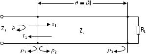
and transmitted multiple times at the two boundaries, as shown in Figure 4.19. Let us first define the reflection and transmission coefficients as follows:
r = total reflection coefficient of the incident wave on the l/4 trans-
|
former |
|
|
r1 |
= reflection coefficient of a wave incident on a load Z t |
from a Z 0 |
|
|
line |
|
|
r2 |
= reflection coefficient of a wave incident on a load Z 0 from a Z t |
||
|
line |
|
|
r3 |
= reflection coefficient of a wave incident on a load R L |
from a Z t |
|
|
line |
|
|
t 1 |
= transmission coefficient of a wave from a Z 0 line into a Z t |
line |
|
t 2 |
= transmission coefficient of a wave from a Z t line into a Z 0 |
line. |
|
According to (4.5) and (4.6), these coefficients can be expressed as
r1 = (Z t − Z 0 )/(Z t + Z 0 )
r2 |
= (Z 0 − Z t )/(Z 0 + Z t ) = −r1 |
r3 |
= (R L − Z t )/(R L + Z t ) |
t 1 = 2Z t /(Z t + Z 0 ) t 2 = 2Z 0 /(Z t + Z 0 )
The total reflection coefficient is obtained as an infinite series of individual reflections and, taking into account that there is a phase shift of e −2ju for each round-trip in the transformer, can be expressed as
Figure 4.19 Multiple-reflection analysis of the l /4 transformer.
92 Radio Engineering for Wireless Communication and Sensor Applications
r = r1 + t1 t 2 r3 e −2ju + t1 t2 r 2 r23 e −4ju + t1 t2 r22 r33 e −6ju + . . .
|
|
|
∞ |
X r 2 r3 e −2ju Cn |
||
= r1 + t1 t 2 r3 e −2ju ∑ |
||||||
|
|
|
n =0 |
|
||
= r1 |
+ |
t 1 t2 r 3 e −2ju |
|
(4.30) |
||
1 |
− r2 r 3 e −2ju |
|||||
|
|
|
||||
The last result is obtained using the sum rule of an infinite geometric series, since | r 2 | < 1 and | r 3 | < 1. If we furthermore take into account that r2 = −r 1 , and t 1 = 1 + r 1 and t2 = 1 − r 1 , we get
|
|
r = |
r1 |
+ r 3 e −2ju |
(4.31) |
|
|
1 + r1 r 3 e −2ju |
|||
|
|
|
|
||
From this we see, because the transformer characteristic impedance |
|||||
is Z t = √ |
Z 0 R L |
and therefore r 1 |
= r3 , and at the center frequency |
||
e −2ju = −1, that the total reflected wave fully disappears at the center fre- |
|||||
quency. If the discontinuities between the impedances Z 0 and Z t as well as
between Z t and R L are small, then | r 1 r3 | << 1, and we can approximate r ≈ r1 + r3 e −2ju.
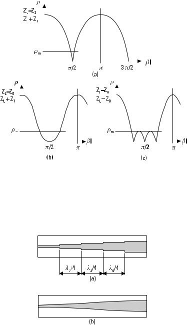
The problem with the quarter-wave transformer is its narrow matching bandwidth. The transformer offers a match only at the frequency where the transformer length is exactly l g /4 (or lg /4 + nlg /2). The bandwidth, over which the reflection coefficient is small, is narrow. Sometimes this is sufficient, but in many applications we need a wider bandwidth.
A wider bandwidth can be obtained by using several consecutive transformer sections, the characteristic impedances of which change with small steps between R L and Z 0 . Depending on how the impedance steps are chosen, different frequency responses of the reflection coefficient are obtained. A binomial transformer provides a maximally flat response. A Chebyshev transformer provides a frequency response where the reflection coefficient fluctuates between certain limits over the matching bandwidth. Figure 4.20 shows the frequency response of a single l /4 transformer, a two-section binomial transformer, and a three-section Chebyshev transformer. The design procedures of the binomial and Chebyshev transformers can be found in many books [3, 4].
Often a l /4 transformer is used to match two lines with different characteristic impedances. Figure 4.21(a) shows how a lowand high-imped-
|
|
|
|
|
|
|
|
|
|
|
|
Impedance Matching |
93 |
||||||||||||||
|
|
|
|
|
|
|
|
|
|
|
|
|
|
|
|
|
|
|
|
|
|
|
|
|
|
|
|
|
|
|
|
|
|
|
|
|
|
|
|
|
|
|
|
|
|
|
|
|
|
|
|
|
|
|
|
|
|
|
|
|
|
|
|
|
|
|
|
|
|
|
|
|
|
|
|
|
|
|
|
|
|
|
|
|
|
|
|
|
|
|
|
|
|
|
|
|
|
|
|
|
|
|
|
|
|
|
|
|
|
|
|
|
|
|
|
|
|
|
|
|
|
|
|
|
|
|
|
|
|
|
|
|
|
|
|
|
|
|
|
|
|
|
|
|
|
|
|
|
|
|
|
|
|
|
|
|
|
|
|
|
|
|
|
|
|
|
|
|
|
|
|
|
|
|
|
|
|
|
|
|
|
|
|
|
|
|
|
|
|
|
|
|
|
|
|
|
|
|
|
|
|
|
|
|
|
|
|
|
|
|
|
|
|
|
|
|
|
|
|
|
|
|
|
Figure 4.20 Reflection coefficient of matching transformers as a function of the transformer section electrical length b l = 2p l /l g : (a) a single l /4 transformer;
(b) a two-section binomial transformer; and (c) a three-section Chebyshev transformer.
Figure 4.21 Matching of a lowand high-impedance coaxial line using (a) a multisection l /4 transformer and (b) a tapered section.