

CHAPTER 15
To Have and to Hold
Several midand high-range PIC devices feature a small EEPROM scratchpad memory that can be controlled and accessed indirectly via SpecialPurpose Registers (SPRs) in the same manner as other peripheral devices. An integral non-volatile scratchpad enables the programmer to read and modify static data, such as the odometer tally in a car, which needs to be retained in the absence of a power supply – see Example 12.3 on page 351. Although this facility can be implemented using an external EEPROM memory, such as the 24LC01 of Fig. 12.22 on page 352, where only a modest amount of non-volatile data needs to be stored, integral EEPROM storage increases reliability and reduces cost, size and power requirements.
Our objective here is to examine the non-volatile storage facilities available to members of the mid-range PIC family. After reading this chapter you will:
•Be familiar with the characteristics of the EEPROM Data memory.
•Know how to both read and write data to the EEPROM module.
•Understand how the main flash EEPROM Program memory can be used in some devices to store and retrieve non-volatile data.
•Be able to contrast the EEPROM Data module and flash Program memory as a location for non-volatile data.
The PIC16C83/4 introduced in 1994, was the first PIC device to use EEPROM technology for its main Program store. As we gave seen in Fig. 2.12 on page 27, Electrically Erasable PROM is similar to EPROM but does not require UV radiation to erase data. Although EEPROM technology is more expensive than EPROM, its use in implementing the Program store is convenient in prototyping and educational/hobbyist applications. Along with this innovation, an EEPROM peripheral module was featured which enabled the programmer to store up to 64 bytes of nonvolatile data independently of the normal file register memory.
The PIC16C83/4 and its analogous flash EEPROM memory successor, the PIC16F83/4, remained the only EEPROM family member until the introduction of the PIC16F87X in 1998. As of 2000, Microchip were committed to introduce flash EEPROM versions of most of their standard midand high-range devices. Thus, for example, the PIC16F74 will shadow the PIC16C74 processor.

 Interrupt on Write complete
 10101010


434 The Quintessential PIC Microcontroller
EECON1 register
7 |
6 |
5 |
4 |
3 |
2 |
1 |
0 |
|
|
|
|
|
|
|
|
|
|
|
|
|
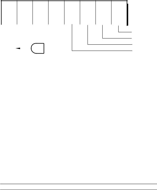
EEIF |
WRERR WREN |
WR |
RD |
|
EECON1 |
||
|
|
|
|
|
|
|
|
|
|
|
|
|
(R/W 0) |
(R/W X) (R/W 0) |
(R/S 0) |
(R/S X) |
File 88h |
|||
|
|
|
|
|
|
|
|
|
|
|
|
|
|
|||||||
|
|
|
|
|
|
|
|
|
|
|
|
|
|
|
|
|
|
|
|
ReaD control |
|
|
|
|
|
|
|
|
|
|
|
|
|
|
|
|
|
|
|
|
|
|
|
|
|
|
|
|
|
|
|
|
|
|
|
|
|
|
|
|
|
WRite control |
Interrupt |
|
|
|
|
|
|
|
|
|
WRite ENable |
||||||||||
|
|
|
|
|
|
|
|
|
|
|||||||||||
|
to CPU |
|
|
|
|
|
|
|
WRite ERRor |
|||||||||||
|
|
|
|
|
|
|
||||||||||||||
|
|
|
|
|
|
|
|
|
|
|
|
|
|
|
|
|
|
|
|
|
|
|
|
|
|
|
|
|
|
|
|
|
|
|
|
|
|
|
R |
= Read |
|
|
|
|
|
|
|
|
|
|
|
|
|
|
6 |
|
INTCON |
|
W = Write |
|||
|
|
|
|
|
|
S |
= Settable |
|||||||||||||
|
|
|
|
|
|
|
|
|
|
|
|
|
EEIE |
|
|
|
||||
|
|
|
|
|
|
|
|
|
|
|
|
|
|
|
|
File 0B h |
|
( ) |
= Reset condition |
|
|
|
|
|
|
|
|
|
|
|
|
|
|
|
|
|
|
||||
Fig. 15.2 The PIC16F8X EECON1 register.
EEPROM CONtrol register 2 EECON2
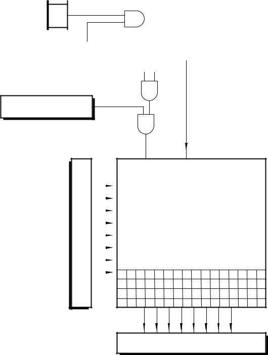
This register located at File 89h is not physically implemented – it always reads as zero. Rather the action of writing the successive code pattern 01010101 → 10101010 with no interruption is used to unlock the Write cycle. This arcane incantation is deliberately designed to convolute the process as security against unintended alterations in the data.
In order to read a specified datum from the EEPROM module we have to implement software to execute the task list:
1.Copy the target cell’s address to EEADR.
2.Set RD to 1 to initiate the Read cycle.
3.RD is automatically cleared immediately and the target 8-bit datum can be read from EEDATA any time from the next instruction cycle as convenient.
Program 15.1 Retrieving a byte from the EEPROM Data module.
; ************************************************************
; * |
FUNCTION: |
Gets one byte from the EEPROM Data module |
* |
|||
; |
* |
ENTRY |
: |
Address in |
EEADR |
* |
; |
* |
EXIT |
: |
Datum in W |
and in EEDATA. System in Bank0 |
* |
; ************************************************************
EE_GET bsf |
STATUS,RP0 |
; Change to Bank1 |
movlw |
b’00000001’ |
; Set RD for Read cycle |
movwf |
EECON1 |
; Read datum into EEDATA |
bcf |
STATUS,RP0 |
; Back to Bank0 |
movf |
EEDATA,w |
; Copy into W |
return |
|
; for return |
|
|
|
15. To Have and to Hold 435
Subroutine EE_GET in Program 15.1 directly implements this process and illustrates the return of the datum from the EEPROM cell to the Working register. The datum will remain in EEDATA until the register is reused.
Writing data to the EEPROM Data module is deliberately made more Byzantine to reduce the chance of a spurious Write corrupting the data due to a software bug or processor malfunction because of, say, a power glitch. The task list to write a datum to a specified cell is:
1.Copy the target cell address to EEADR.
2.Set WREN in EECON1[2] to enable the Write process.
3.Disable all interrupts.
4.Send 55hto EECON2.
5.Send AAhto EECON2.
6.Set WR to initiate the Write cycle.
7.Clear WREN.
8.Enable interrupts.
9.Wait until WR returns to zero, signalling the completion of the Write cycle, and exit.
The Write cycle will not initiate if the interlock sequence items 4 – 6 is not exactly followed without interference. For example; in an interruptdriven system an interruption during the interlock sequence will abort the Write cycle. Thus in this situation interrupts should be disabled by clearing GIE until the Write cycle has been initiated, otherwise this step can be omitted.
If desired the completion of the Write cycle can be used to interrupt the processor. This is enabled by setting the EEIE mask bit in INTCON[6]. When the interrupt flag EEIF, located in EECON1[4], is set in the normal way then the interrupt is generated. It should be cleared in the ISR.
It is possible that the processor is reset, for example by a Watchdog overflow, before the Write cycle is complete. In this situation, the EEPROM datum may be corrupt. The WRERR flag in EECON1[3] will be set if the Write operation has been prematurely terminated with a Reset action. If this is not the case, when the cycle is complete the datum may be read back and verified to give extra security. The WREN bit may be cleared at this point to help prevent an accidental Write. Doing this before the Write is complete will not a ect the operation.
Program 15.2 implements this task list. Both EEDATA and EEADR are set up by the caller program with the byte data and address. The subroutine is not pulled out until the Write cycle has completed; typically 4 ms. This ensures that these SPRs will not be altered during the cycle which may possibly give an erroneous outcome.
In order to illustrate these concepts we will repeat Example 12.3 on page 351 replacing the external serial EEPROM with the internal module. We will assume that the odometer count is located at EEPROM cells 10
– 12h.

436 The Quintessential PIC Microcontroller
Program 15.2 Putting a byte into the EEPROM Data module.
; ************************************************************
; * |
FUNCTION: |
Writes one byte into the EEPROM Data module |
* |
||
; * |
ENTRY |
: |
Datum byte in EEDATA, module address in EEADR |
* |
|
; |
* |
EXIT |
: |
Interrupts disabled for 9 instructions |
* |
; |
* |
EXIT |
: |
System in Bank0 |
* |
; ************************************************************
EE_PUT |
bsf |
STATUS,RP0 |
; |
Change to Bank1 |
|
bsf |
EECON1,WREN |
; |
Enable for Write cycle |
EE_LOOP |
bcf |
INTCON,GIE |
; |
Disable all interrupts |
|
btfsc |
INTCON,GIE |
; |
Check, did it clear? |
|
goto |
EE_LOOP |
; |
IF not THEN do again |
|
movlw |
55h |
; |
Now do the interlock |
|
movwf |
EECON2 |
|
|
|
movlw |
0AAh |
|
|
|
movwf |
EECON2 |
|
|
|
bsf |
EECON1,WR |
; |
Initiate the Write cycle |
|
bcf |
EECON1,WREN |
; |
Optionally disable any other Writes |
|
bsf |
INTCON,GIE |
; |
Re-enable interrupts |
EE_EXIT |
btfsc |
EECON1,WR |
; |
Check, has the Write completed? |
|
goto |
EE_EXIT |
; |
IF not THEN retry |
|
bcf |
STATUS,RP0 |
; |
Go back to Bank0 |
|
return |
|
; |
and return when cycle has finished |
|
|
|
|
|
The coding shown in Program 15.3 makes use of the two subroutines EE_GET and EE_PUT to read and subsequently write the three odometer bytes from the EEPROM Data module. The address of the first (highest) byte is copied into EEADR at the beginning of the subroutine and is subsequently incremented and decremented in situ to point to the appropriate datum.
Once the 3-byte odometer state has been fetched and copied into memory it is incremented in exactly the same manner as in Program 12.15 on page 354. The augmented array is then written back into EEPROM in the opposite sense as it was read, with EEADR being decremented. The EE_PUT subroutine checks that the Write cycle has been completed before returning and thus timing need not be checked by the calling program.
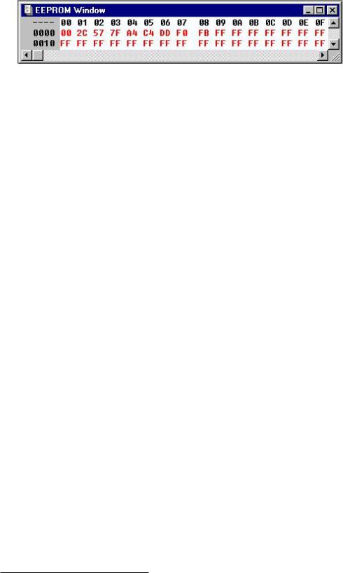
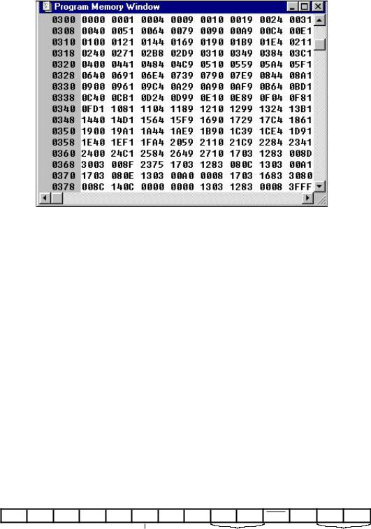
As well as altering data under program control it is possible to initialize the state of the EEPROM Data module when the executable program is being externally blasted into the Program memory; as illustrated in Fig. 10.5(a) on page 261. The area of Program memory beyond the user Program store belongs to the special test/configuration memory space 2000h– 30FFh and can be accessed only during external programming. In Fig. 10.5(b) we observed that the Configuration fuse word is located at 2007h. The EEPROM module also lies in this space located at 2100h– 21FFh. For example, to store the value of sine every 10◦ between 0◦ and 90◦ as part of the program source code we have:
|
|
15. To Have and to Hold 437 |
|
|
|
org |
2100h |
; The EEPROM Data module |
SINE de |
0, 2Ch, 57h, 7Fh, 0A4h, 0C4h, 0DDh, 0F0h, 0FBh, 0FFh |
|
|
|
|
where the assembler directive de (Data EEPROM) specifies the comma delimited list of data. Once the PIC has been programmed, the contents of the EEPROM Data module will look like Fig. 15.3.
Program 15.3 Incrementing the non-volatile odometer count in Data EEPROM.
;************************************************************
;FUNCTION: Adds one onto the triple-precision odometer total*
; RESOURCE: |
Subroutines |
EE_GET and |
EE_PUT |
* |
|||
; ENTRY |
: |
Current total in EEPROM module at 10:11:12h |
* |
||||
; |
EXIT |
: |
Incremented |
total |
back |
in EEPROM module |
* |
; |
EXIT |
: |
also available in |
RAM at LSB:NSB:MSB |
* |
||
; ************************************************************
EXTRA_MILE movlw movwf call movwf incf call movwf incf call movwf
; Now increment 3-byte array
incf |
LSB,f |
; Add one |
btfss |
STATUS,Z |
; Is it now zero |
goto |
PUT_BACK |
; IF not THEN continue |
incfsz |
NSB,f |
; Increment middle byte |
goto |
PUT_BACK |
; IF not zero THEN continue |
incf |
MSB,f |
|
; Put the augmented odometer count back in Data EEPROM
PUT_BACK movf |
LSB,w |
; Get new odometer low byte |
movwf |
EEDATA |
; Put in EE Data register |
call |
EE_PUT |
; Write to EEPROM cell 12h |
decf |
EEADR,f |
; Address of middle byte |
movf |
NSB,w |
; Get new odometer middle byte |
movwf |
EEDATA |
; Put in EE Data register |
call |
EE_PUT |
; Write to EEPROM cell 11h |
decf |
EEADR,f |
; Address of high byte |
movf |
MSB,w |
; Get new odometer low byte |
movwf |
EEDATA |
; Put in Data register |
call |
EE_PUT |
; Write to EEPROM cell 10h |
return |
|
|
|
|
|
15. To Have and to Hold 439
PIC16F874
This 40-pin device has a 8 Kbyte flash Program store and 256-byte EEPROM Data store together with 192 file registers. It is pin compatible with the PIC16C74 device.
PIC16F876
This 28-pin device is the same as the PIC16F873 but with twice the Program store capacity at 8 Kbytes and double the EEPROM Data module capacity at 256 bytes The file register store is increased to 368 file registers.
PIC16F877
This is a 40-pin version of the PIC16F876. Key EEPROM properties are:
•100,000 minimum EEPROM Data module Erase/Write cycle endurance per cell.
•1000 minimum flash EEPROM Program store Erase/Write cycle endurance.
•Maximum Write/Erase time 8 ms (typical 4 ms) for both the Data module and flash memory.
Of particular note is the endurance limit of 1000 Write cycles for the flash EEPROM. Whilst this is entirely satisfactory when changing the device’s program, it is a limitation for some non-volatile data storage situations. Thus flash Program memory storage is more applicable to constant data, such as the sine lookup table, rather than for information that requires frequent update, such as the odometer.
Flash EEPROM has a smaller geometry than normal EEPROM. Whilst this speeds up its operation, charges which eventually trap in the floating gate insulation have a disproportional e ect on the storage mechanism and leads to earlier deterioration.
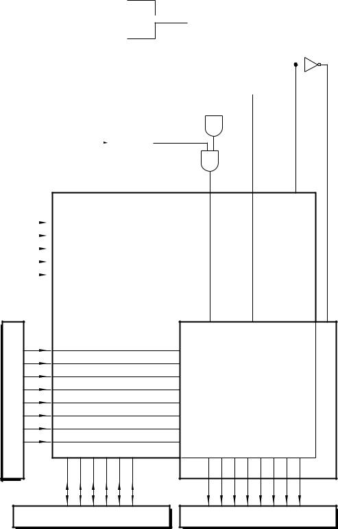
Figure 15.4 shows the PIC16F87X EEPROM Data module with the flash Program store superimposed. This form of representation is used as the EEDATA and EEADR registers are common to both EEPROM arrays. Of course, the flash Program store is larger both in the number of cells (8 Kbytes against 256 bytes) and in cell size (14 bits against 8 bits). Thus both Data and Address registers have the high-end extensions EEDATH and EEADRH respectively to cope with this additional capacity.
As we shall see, the process of reading from and writing to either array is similar. The target module is chosen using the EEPGD (EEProgram/Data) control bit control bit in EECON1[7]. Apart from this additional bit and the removal of the EEIF interrupt flag to the PIR2 register, the EECON1 register of Fig. 15.5 is identical to the basic PIC16F8X version shown in Fig. 15.2. The virtual EECON2 interlock register remains the same.

 Interrupt on Write complete


442 The Quintessential PIC Microcontroller
Program 15.4 Reading a word from the flash Program store.
; ************************************************************
; * |
FUNCTION: |
Gets one byte from the flash Program store |
* |
||
; |
* |
ENTRY |
: |
Address in EEADRH:EEADR |
* |
; |
* |
EXIT |
: |
Datum in EEDATH:EEDATA. System in Bank0 |
* |
; ************************************************************
FLASH_GET |
|
|
bsf |
STATUS,RP1 |
; Change to Bank3 |
bsf |
STATUS,RP0 |
|
movlw |
b’10000000’ |
; Point to Program memory |
movwf |
EECON1 |
; by setting EEPGD |
bsf |
EECON1,RD |
; Set RD for Read cycle |
nop |
|
; Dummy nops |
nop |
|
|
bcf |
STATUS,RP1 |
; Return to Bank0 |
bcf |
STATUS,RP0 |
|
return |
|
|
|
|
|
The Write cycle also is virtually identical to its Data module counterpart but with the addition of a double-nop relaxation phase. This gives us our flash Write cycle task list:
1.Copy the target cell address to EEADRH:EEADR.
2.Set WREN in EECON1[2] to enable the Write process.
3.Disable all interrupts.
4.Send 55hto EECON2.
5.Send AAhto EECON2.
6.Set WR to initiate the Write cycle.
7.Execute two dummy nop instructions.
8.Clear WREN.
9.Enable interrupts.
10.Wait until WR returns to zero, signalling the completion of the Write cycle, and exit.
The subroutine FLASH_PUT in Program 15.5 assumes that the cell address is in EEADRH:EEADR and 14-bit datum is in EEDATH:EEDATA on entry.
For our example we will design a subroutine that will return the square of an integer between 0 and 100 in EEDATH:EEDATA. We could of course calculate this by multiplication, but for the purposes of this exercise we will implement this exercise as a look-up table located in flash Program store. As this is a table of constants we can load the data into flash memory at the same time as the rest of the program code.
In Program 15.6 the table is located at 300h in the Program store. The directive dw (Data Word) is similar to de but each datum in the comma separated list is 14-bits. For convenience the radix directive is used to specify constants by default are treated as decimal.

15. To Have and to Hold 443
Program 15.5 Writing to flash Program memory.
; ************************************************************
; * |
FUNCTION: |
Writes one |
byte into the flash Program store |
* |
|||
; * |
ENTRY |
: |
Datum |
byte |
in EEDATH:EEDATA |
* |
|
; * |
ENTRY |
: |
Datum |
address in EEADRH:EEADR |
* |
||
; |
* |
EXIT |
: |
Interrupts |
disabled for 11 instructions |
* |
|
; |
* |
EXIT |
: |
System in Bank0 |
* |
||
; ************************************************************
FLASH_PUT bsf |
STATUS,RP0 |
; |
Go to Bank 3 |
bsf |
STATUS,RP1 |
|
|
bsf |
EECON1,EEPGD; |
Target the flash Program store |
|
bsf |
EECON1,WREN |
; |
Enable for Write cycle |
FLASH_LOOP bcf |
INTCON,GIE |
; |
Disable all interrupts |
btfsc |
INTCON,GIE |
; |
Check, did it clear? |
goto |
FLASH_LOOP |
; |
IF not THEN do again |
movlw |
55h |
; |
Now do the interlock |
movwf |
EECON2 |
|
|
movlw |
0AAh |
|
|
movwf |
EECON2 |
|
|
bsf |
EECON1,WR |
; |
Initiate the Write cycle |
nop |
|
; |
Dummy nops |
nop |
|
|
|
bcf |
EECON1,WREN |
; |
Disable any more Writes |
bsf |
STATUS,GIE |
; |
Re-enable interrupts |
FLASH_EXIT |
|
|
|
btfsc EECON1,WR |
; |
Check, has the Write completed? |
|
goto FLASH_EXIT |
; |
IF not THEN retry |
|
bcf |
STATUS,RP1 |
; |
Go back to Bank 0 |
bcf |
STATUS,RP0 |
|
|
return |
|
; |
& return when cycle has finished |
|
|
|
|
Directly following the table is the executable code. In this manner Program 15.6 is comparable to a C++ class where a program object comprises both data members and member functions (subroutines).
The subroutine itself builds up the table element nn address by placing the integer passed in W in EEADR and the constant 03h in EEADRH. This gives the double-byte address as 3nnh. Once this is done, the subroutine FLASH_GET retrieves the 14-bit datum from the table. The subroutine then moves both bytes from EEDATH:EEDATA and returns the datum in the two file registers SQRH:SQRL in Bank 0. Unlike the PIC16F8X, general-purpose file registers are not reflected across the various banks, so each byte copied from EEPROM SPRs in Bank 2 needs switching to Bank 0 once the byte has reached the Working register.
When the program has been burnt into flash memory by the external programmer the Program store in the area around 300h will look like Fig. 15.6.

444 The Quintessential PIC Microcontroller
Program 15.6 Squaring an integer.
__config _CPD_OFF & _WRT_ENABLE_OFF org 300h
; ************************************************************
; * |
FUNCTION: |
Generates the square |
of |
an integer |
* |
|||
; * |
RESOURCE: |
Subroutine |
FLASH_GET |
|
|
* |
||
; |
* |
ENTRY |
: |
Integer in |
W range 0 |
-- |
100 |
* |
; |
* |
EXIT |
: |
14-bit square in SQRH:SQRL. In Bank0 |
* |
|||
; ************************************************************
TABLE
dw 0,1,4,9,16,25,36,49,64,81,100,121,144,169,196,225
dw 256,289,324,361,400,441,484,529,576,625,696,729,784,841 dw 900,961,1024,1089,1156,1225,1296,1369,1444,1521,1600,1681 dw 1764,1849,1936,2025,2116,2209,2304,2401,2500,2601,2704
dw 2809,2916,3025,3136,3249,3364,3481,3600,3721,3844,3969 dw 4049,4225,4356,4489,4624,4761,4900,5041,5184,5329,5476 dw 5625,5776,5929,6084,6241,6400,6561,6724,6889,7056,7225 dw 7396,7569,7744,7921,8100,8281,8464,8649,8836,9025,9216 dw 9409,9604,9801,10000
SQUARE bsf |
STATUS,RP1 |
; Move to Bank2 |
bcf |
STATUS,RP0 |
|
movwf |
EEADR |
; Build up the address |
movlw |
3 |
|
movwf |
EEADRH |
|
call |
FLASH_GET |
; Get table entry n in 3nnh |
bsf |
STATUS,RP1 |
; Move back to Bank2 |
bcf |
STATUS,RP0 |
|
movf |
EEDATA,w |
; Get lower byte of square |
bcf |
STATUS,RP1 |
; Bank0 |
movwf |
SQRL |
; Copy to SQRL in Bank0 |
bsf |
STATUS,RP1 |
; Back to Bank2 |
movf |
EEDATH,w |
; Get high byte of square |
bcf |
STATUS,RP1 |
; Bank0 |
movwf |
SQRH |
; and copy to SQRH in Bank0 |
return |
|
|
|
|
|
Like the PIC16F8X, as discussed on page 260, the PIC16F87X line has code protection fuses in its configuration word – as shown in Fig. 15.7. The primary function of code protection is to prevent the external programmer reading code from the Program store to give a measure of security against unauthorized peeking at the code. In the case of the PIC16F87X devices two code bits (duplicated as bits 13:12 and 5:4) in the configuration word in the special/test configuration area at 2007h give protection for all the Program store (00), the top half of the store (01), the top 256 bytes only (10) or no protection (11); the default situation. If protection is given to any area of memory then the external programmer cannot subsequently write data into anywhere in the Program store nor

446 The Quintessential PIC Microcontroller
Although the table has here been placed at an even 256-byte boundary for convenience, in practice it can be located anywhere in memory. In the general case the table o set nn will need to be added to the 14-bit address TABLE. SAQ 15.2 discusses how this address arithmetic could be done.
Examples
Example 15.1
The CCS compiler has the following built-in functions dealing with the EEPROM Data module:
read_eeprom(address)
Reads a byte from the specified EEPROM address.
write_eeprom(address, value)
Write the value to the specified address and returns only when the Write cycle has finished.
Write a C function to duplicate the odometer update implemented at assembler level in Program 15.3.
Solution
Like its assembly-level counterpart of Program 15.3, the function of Program 15.7 is divided into three phases.
1.This phase creates an array of three bytes named odometer[] which will act as a temporary store for the odometer count located in EEPROM. As the EEPROM Data module handles data in discrete byte
Program 15.7 C-based coding for the odometer.
void odometer(void) |
|
|
{ |
|
|
unsigned int odometer[3]; |
/* Define the 3-byte count |
*/ |
odometer[0] = read_eeprom(0x10); /* Get the existing count |
*/ |
|
odometer[1] = read_eeprom(0x11); |
|
|
odometer[2] = read_eeprom(0x12); |
|
|
/* Increment array |
|
*/ |
if(++odometer[0] != 0) break; |
|
|
else if(++odometer[1] != 0) break; |
|
|
else odometer[2]++; |
|
|
/* Now return incremented count to the EEPROM |
*/ |
|
write_eeprom(0x10, odometer[0]); |
|
|
write_eeprom(0x11, odometer[1]); write_eeprom(0x12, odometer[2]);
}
15. To Have and to Hold 447
packages, it is best to model the object in C in the same manner. The array is given the current reading by extracting the data one byte at a time from EEPROM locations 10:11:12h using the read_eeprom() function.
2.Once the 3-byte data is in the Data store it is incremented using an if-else tree:
(a)Increment low byte and check for zero. IF not zero THEN the overall addition is complete ELSE pass on carry to next byte.
(b)Increment the middle byte and check for zero. IF not zero THEN the overall addition is complete ELSE pass on carry to next byte.
(c)Increment most significant byte.
3.Finally each byte is written back into the EEPROM Data module using the write_eeprom() function.
Comparing the hand-coded assembly of Program 15.3 against the code generated from Program 15.7 gives 52 instructions against 91.
Example 15.2
A feasibility study is being undertaken in using a PIC-based Sauna controller. This is to monitor temperature and control heating and cooling units. There is also to be an over-temperature emergency alarm and shut- o .
One possibility is to use an 8-pin PIC with integral A/D conversion, such as the PIC12C672, together with an external temperature transducer. Someone has suggested that an e cient approach to this problem would be to use the variation in the internal Watchdog timer’s period with temperature as a cost e ective, albeit crude, sensor.
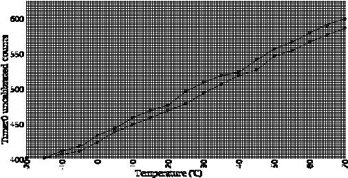
Experimental data was collected using a sample of eight production devices from the same manufacturing lot, with a soak time of 30 minutes at each tested temperature and 500 uncalibrated periods averaged to produce the graph of Fig. 15.8.
The data presented in Fig. 15.8 is based on Microchip’s application note AN720 Measuring Temperature Using the Watch Dog Timer (WDT). The two loci give the maximum and minimum across the range of tested devices. The Watchdog period was measured in Timer 0 overflows counting an internal 4 MHz clock. The Watchdog timer used a 1:8 prescale ratio.
From this data it can be seen that there is a correlation between period and rising temperature. However, although the overall trend is predictable, di erent devices will have varying o sets and slopes. For example, within the eight devices tested here the scale factor (scalar) varies from 2.28–2.42 counts per degree Celsius. This will necessitate a calibration phase before the system is used. If the count at one temperature T0 and the scalar are known for any device, then for the specific case where a count COUNTn − COUNT0 is recorded:
∆T = (COUNTn − COUNT0) × Scalar
448 The Quintessential PIC Microcontroller
Fig. 15.8 Watchdog timer period versus temperature.
In order to calibrate these devices it has been decided to soak batches in a refrigerator at 0◦C and save the 2-byte count in the EEPROM data module of a PIC16F83. The soak test is to be repeated in an oven at 30◦C with the di erence between this second count and the original value to be stored in a single EEPROM byte. Once this has been done, the device can be reprogrammed with the final running program overwriting the original calibrate program. This running program can then calculate temperature using the actual Watchdog period COUNTn:
T = (COUNT0 − COUNTn) × (Di erence/30)
where COUNT0 is the 2-byte EEPROM datum showing the count at 0◦C and Di erence is the 1-byte EEPROM datum showing the change in count over 30◦C.
Show how you could code the calibrate program to implement this specification.
Solution
Five tasks can be identified which must be undertaken at the end of a Watchdog period.
•Average the current Timer 0 roll-over count with the existing low-temp- erature (i.e. 0◦C) count.
•Average the current Timer 0 roll-over count with the existing hightemperature (i.e. 30◦C) count.
•Store the low-temperature count in EEPROM.
•Calculate the di erence between lowand high-temperature count and store in EEPROM.
•Do nothing.
15. To Have and to Hold 449
Port lines can be used to signal which of the first four active actions are to be actioned. For example; if RA0 is high then add the current Timer 0 rollover count to the existing 2-byte low-temperature count. Unless this is the first reading, divide by two to give an average. The complete batch of devices could have their RA0 pin held high for a few minutes 30 minutes after the refrigerator stabilizes at 0◦C.
Bringing RA0 low and then RA2 high for a short time signals an EEPROM storage action. With all port lines low, no action is taken representing both time before temperature stabilization and after EEPROM programming.
The Timer 0 and Watchdog timers are initialized together with the count values on a once-only basis on Power-up reset. This will typically only occur when the devices are powered up when in the temperature bath. Subsequent resets will normally be due to Watchdog time-outs. The state of the Status register’s TO flag can be used to ascertain the source of reset – see page 363.
Program 15.8 shows the routine used to initialize the timers and variables entered if TO is 1 on reset; that is on Power-up. Once this is done, the system enters an endless loop goto $ (the assembler replaces the label $ by the instruction’s address) which simply keeps going to itself!
Also shown is the ISR servicing a Timer 0 interrupt. This increments the double-byte variable ROLL_OVER:ROLL_OVER+1 and this is the count value read by the system on a Watchdog reset giving a numerical value for period.
Eventually the Watchdog timer will time-out and reset the processor. This time TO will be 0 and the routine labelled READING in Program 15.9 will be entered. This checks the state of each of the four RA3:0 pins in turn, executing one of the four listed tasks. If no pin is high, the program simply clears ROLL_OVER:ROLL_OVER+1 and Timer 0, the Watchdog timer is restarted and an endless loop entered. This READING_EXIT routine is also entered at the end of the four tasks.
The first two tasks are shown in Program 15.9. Here the 2-byte Timer 0 roll-over count is either added to the existing value LO_TEMP:LO_TEMP+1 or HI_TEMP:HI_TEMP+1 as appropriate and the outcome shifted once right to divide by two to give the average. As the count total is modest, 2-byte arithmetic is su cient to avoid overflow. If this is repeated over a duration of several minutes an averaged value will result.
If this is the very first time a reading has been made then the divide by two operation is skipped and the flag variable FIRST_LO or FIRST_HI as appropriate is made non zero.
The core routine with respect to this chapter is given in Program 15.10. If RA2 is 1 the 2-byte low-temperature count LO_TEMP:LO_TEMP+1 is copied into the bottom two bytes of the EEPROM Data module using the EE_PUT subroutine of Program 15.2.

450 The Quintessential PIC Microcontroller
Program 15.8 The Sauna Power-up reset sequence and ISR.
|
__config _WDT_ON & _CP_OFF & _RC_OSC |
|||
|
cblock |
20h |
|
|
|
_work:1, _status:1 |
|
|
|
|
FIRST_HI:1, FIRST_LO:1 |
|
||
|
ROLL_OVER:2, LO_TEMP:2, HI_TEMP:2 |
|||
|
DELTA_TEMP:1 |
|
|
|
|
endc |
|
|
|
|
org |
0 |
|
|
START |
goto |
MAIN |
|
|
|
org |
4 |
|
|
|
goto |
ISR |
|
|
MAIN |
btfss |
STATUS,NOT_TO |
; |
IF Watchdog timeout |
|
goto |
READING |
; |
THEN must have a reading |
|
clrwdt |
|
|
|
|
movlw |
b’11011010’ |
; |
Wdt enabled with a 1:8 prescale |
|
bsf |
STATUS,RP0 |
; |
Change to Bank1 |
|
movwf |
OPTION_REG |
; |
and TMR0 internal clock |
|
bcf |
STATUS,RP0 |
; |
and back to Bank0 |
|
clrf |
FIRST_HI |
|
|
|
clrf |
FIRST_LO |
|
|
|
bsf |
INTCON,T0IE |
; |
Enable Timer0 interrupt |
|
clrf |
TMR0 |
; |
Zero the Timer |
|
clrf |
ROLL_OVER+1 |
; |
Zero the 2-byte Timer roll-over |
|
clrf |
ROLL_OVER |
|
|
|
bsf |
INTCON,GIE |
; |
Enable all interrupts |
|
goto |
$ |
; |
Endless loop |
; |
************************************************************** |
|
; |
* The ISR to increment the 2-byte COUNT IF TMR0 interrupt |
* |
;**************************************************************
;First save context in usual way
ISR |
movwf |
_work |
; Put |
away W |
|
swapf |
STATUS,w |
; and |
the Status register |
|
movwf |
_status |
|
|
;**************************************************************
;The core code
incf |
ROLL_OVER+1,f; |
Record one more roll-over |
||
btfsc |
STATUS,C |
; |
Skip if no carry |
|
incf |
ROLL_OVER,f |
; |
Increment upper |
byte |
bcf |
INTCON,T0IF |
; |
Clear interrupt |
flag |
; **************************************************************
swapf |
_status,w |
; Untwist |
the original Status reg |
||
movwf |
STATUS |
|
|
|
|
swapf |
_work,f |
; Get |
the |
original W reg back |
|
swapf |
_work,w |
; |
leaving |
STATUS unchanged |
|
retfie |
|
; |
and |
return from interrupt |
|
|
|
|
|
|
|

15. To Have and to Hold 451
If RA3 is 1 the di erence between the 2-byte high and low temperatures is then calculated. With the data shown in Fig. 15.8 it can be seen that a 30◦C di erence will not exceed a byte’s worth of storage so only the
Program 15.9 Reading a new period count.
READING |
btfsc |
PORTA,0 |
; |
Check; new low temp desired? |
|
goto |
NEW_LO |
; |
IF yes THEN go to it! |
|
btfsc |
PORTA,1 |
; |
Check; new high temp desired? |
|
goto |
NEW_HI |
; |
IF yes THEN go to it! |
|
btfsc |
PORTA,2 |
; |
Check; update low temp desired? |
|
goto |
UPDATE_LO |
; |
IF yes THEN go to it! |
|
btfsc |
PORTA,3 |
; |
Check; update high temp desired? |
|
goto |
UPDATE_HI |
; |
IF yes THEN go to it! |
|
goto |
READING_EXIT ; |
ELSE nothing doing |
|
NEW_LO |
movf |
ROLL_OVER+1,w; |
ELSE get low byte TMR0 roll-over |
|
|
addwf |
LO_TEMP+1,f |
; |
and add it to low byte low temp |
|
btfsc |
STATUS,C |
; |
Check for Carry |
|
incf |
LO_TEMP,f |
; |
IF so THEN record it |
|
movf |
ROLL_OVER,w |
; |
Now get high byte of roll-over |
|
addwf |
LO_TEMP,f |
; |
and add it to high byte low temp |
|
movf |
FIRST_LO,f |
; |
Is this the 1st low reading? |
|
btfsc |
STATUS,Z |
|
|
|
goto |
FIRST_TIME_LO; |
IF so THEN go to it! |
|
|
rrf |
LO_TEMP,f |
; |
ELSE divide sum by two |
|
rrf |
LO_TEMP+1,f |
|
|
|
goto |
READING_EXIT ; |
and finished |
|
FIRST_TIME_LO |
|
; |
IF first reading simply transfer |
|
|
incf |
FIRST_LO,f |
; |
No longer the first reading |
|
goto |
READING_EXIT |
|
|
NEW_HI |
movf |
ROLL_OVER+1,w; |
ELSE get low byte TMR0 roll-over |
|
|
addwf |
HI_TEMP+1,f |
; |
and add it to low byte high temp |
|
btfsc |
STATUS,C |
; |
Check for Carry |
|
incf |
HI_TEMP,f |
; |
IF so THEN record it |
|
movf |
ROLL_OVER,w |
; |
Now get high byte of roll-over |
|
addwf |
HI_TEMP,f |
; |
and add it to high byte high temp |
|
movf |
FIRST_HI,f |
; |
Is this the 1st high reading? |
|
btfsc |
STATUS,Z |
|
|
|
goto |
FIRST_TIME_HI; |
IF so THEN go to it! |
|
|
rrf |
HI_TEMP,f |
; |
ELSE Divide sum by two |
|
rrf |
HI_TEMP+1,f |
|
|
|
goto |
READING_EXIT ; |
and finished |
|
FIRST_TIME_HI |
|
; |
IF first reading simply transfer |
|
|
incf |
FIRST_HI,f |
; |
No longer the first reading |
READING_EXIT |
|
|
|
|
|
clrf |
TMR0 |
; |
Zero the timer |
|
clrwdt |
|
; |
Reset the Watchdog timer |
|
clrf |
ROLL_OVER+1 |
; |
Zero the roll-over count |
|
clrf |
ROLL_OVER |
|
|
|
goto |
$ |
; |
Wait for another Watchdog reset |
|
|
|
|
|

452 The Quintessential PIC Microcontroller
Program 15.10 Updating the Sauna EEPROM.
UPDATE_LO |
|
|
|
movf |
LO_TEMP,w |
; Get high byte of low temperature |
|
bsf |
STATUS,RP0 |
; To Bank1 |
|
movwf |
EEDATA |
; In EEPROM Data register |
|
clrf |
EEADR |
; EEPROM address 00h |
|
call |
EE_PUT |
; Write datum in |
|
movf |
LO_TEMP+1,w |
; Get low byte of low temperature |
|
bsf |
STATUS,RP0 |
; To Bank1 |
|
movwf |
EEDATA |
; Is new datum |
|
incf |
EEADR,f |
; EEPROM address 01h |
|
call |
EE_PUT |
; Write Datum in |
|
goto |
READING_EXIT |
|
|
UPDATE_HI ; |
Work out HI_TEMP-LO_TEMP & store at 02 in EEPROM |
||
; Only need |
to subtract the lower bytes as diff fits in one byte |
||
movf |
HI_TEMP+1,w |
; Get low byte high temperature |
|
subwf |
LO_TEMP+1,w |
; Subtract low byte low temperature |
|
movwf |
DELTA_TEMP |
; giving the difference |
|
bsf |
STATUS,RP0 |
; To Bank1 |
|
movwf |
EEDATA |
; Delta temperature in 02h |
|
movlw |
2 |
|
|
movwf |
EEADR |
|
|
call |
EE_PUT |
|
|
goto |
READING_EXIT |
|
|
lower byte of the subtraction is implemented. This single byte di erence is then written into EEPROM in the normal way.
Self-assessment questions
15.1Good program practice dictates that the datum written into Data EEPROM should be verified as the value that was intended to be written. Show how you could modify the EE_PUT subroutine of Program 15.2 to return a value −1 in a file register if the action is not successful, otherwise zero.
15.2In Program 15.6 we placed the look-up table at a 256-byte boundary in the Program store (specifically 300h) to simplify the computation of the 1-byte table index. Thus to look up table entry nn we simply place the address 3nnh in the EEADRH:EEADR register pair.
Placing program segments at user-defined addresses is never a good idea, as subsequential program alterations can cause code to overlap unless care is taken. Letting the assembler sort out loca-

15. To Have and to Hold 453
tions of labels is much more reliable. However, in our case we would need to add nn to the address the assembler selects for the label TABLE. Unfortunately Program store addresses are 13-bits wide and PIC arithmetic is only 8-bit. Microchip compatible assemblers have the directives high and low to separate the upper and lower bytes parts of a label; eg. movlw low TABLE. Using these directives modify the subroutine SQUARE if the directive org 300h is removed.
15.3 Microchip-compatible assemblers have the directive da (DAta) which can be used to store strings of character codes in Program memory. For example:
MESSAGE da "Hello world/n",0
which places the codes characters in quotes coded in 7-bit ASCII code packed two at a time in each 14-bit word followed by all zeros. The \n escape character means New Line – ASCII code 0Ah.
Assuming that this is done in a PIC16F87X device, write a subroutine called PDATA (Print DATA) to fetch each character from Program memory and transmit to a terminal using the subroutine PUTCHAR of Program 12.11 on page 340.
15.4 A certain hotel security system is to use a PIC-based reprogrammable smart card for electronic guest room locks. On registration the card is to be charged up with the following details:
1.A 4-digit room number, eg. 1311.
2.Start data, eg. 13072000.
3.End date, eg. 15072000.
Assume that the PIC has an integral EEPROM Data module and communicates with the receptionist’s terminal via a serial input subroutine, such as described in Program 12.11 on page 340. Data is coded in ASCII in the order outlined, preceded with the character STX, terminated by ETX and delimited by SP – see Table 1.1 on page 5. Design a routine to interpret the data and store them in EEPROM.