Добавил:
Опубликованный материал нарушает ваши авторские права? Сообщите нам.
Вуз: Предмет: Файл:
Katzen S.The quintessential PIC microcontroller.2000.pdf
Скачиваний:
26
Добавлен:
23.08.2013
Размер:
3.92 Mб
Скачать

PART III

The Outside World

Apart from our brief discussion of the Havard structure in Chapter 3, we have confined our discussions to the internal structure of the microcontroller and its software. This final part looks at how the MCU core interacts with the environment physically beyond the confines of its pins. This process involves consideration of the interaction of the software and hardware of its integrated ports and devices, ending up with a case study which builds a complete stand-alone embedded controller. We will mainly concentrate on the PIC16F84 mid-range device but will breifly look at other devices where that is pertinent. On the way you will:

Look at support issues such as the power supply, clock, power management and device configuration.

Consider parallel and serial digital data input and output.

The Timer and Watchdog subsystems.

See what is involved in dealing with analog signals.

Examine relevant interrupt-handling issues in real-time interactions.

Design an embedded MCU-based viva timer.

Consider how a system may be tested and debugged.

CHAPTER 10

The Real World

Up to this point we have mainly concentrated on how the software has interacted with the processor’s internal registers and Data memory. Now, as a prelude to how the MCU relates to its internal peripheral devices and hence monitors and controls its external environment, i.e. the real world outside its pins, we need to look at external support issues, such as power supply requirements, clocking and resetting.

After reading this chapter you will:

Be familiar with the permitted range of power supply and input/output voltages.

Distinguish between quiescent and dynamic power dissipation and recognize that the latter is directly proportional to both frequency and to the square of the supply voltage.

Be aware of how the sleep mode is invoked and exited, and its e ect on the processor.

Understand the basics of the integral clock oscillator.

Know how the PIC’s configuration can be set up during programming.

Understand the various nuances of the Reset process.

Figure 10.1 gives the external view of some typical PIC family members, ranging from the minuscule 8-pin 12-bit PIC12C508/9, which features one 5-bit general-purpose parallel I/O port, a Timer and 12 Kbyte Program store and 25/41 file registers through to the jumbo 40-pin 14bit PIC16F877 which has a 8 Kbyte flash memory Program store, 368 file registers, 33 bits of parallel I/O, three Timers, a 10-bit A/D converter, several serial port formats and a 256-byte EEPROM Data module. We are going to mainly concentrate on the 18-pin PIC16F83/41 and the 40-pin PIC16C74, but most of the characteristics are similar across all PIC families. Where relevant, other family members will be used as the exemplar; particularly the PIC16C7X and PIC16F87X devices.

All members of the PIC family will operate typically with a supply voltage VDD of nominally 5 V. The standard PIC16F84 can operate over

1The PIC16F83 is identical to the PIC16F84 but has 50% less Program memory and 36 instead of 68 file registers. The latter is currently available as the PIC16F84A with minor enhancements.

254 The Quintessential PIC Microcontroller

GP2/T0CKI

5


4

GP3/MCLR


RB4

10


9

RB3


GP1

6


3

GP4/OSC2


RB5

11


8

RB1


12


7


GP0

7


2

GP5/OSC1/CLOCK


RB6


RB0/INT


8


1


VSS


VDD


RB7

13


6

VDD


(a) PIC12C508/9


VDD

14


5

VSS


OSC2/CLKOUT

15


4

MCLR


OSC1/CLKIN

16


3

RA4/T0CKI


RD2/PSP2

21


20

RD1/PSP1


RA0

17


2

RA3


RD3/PSP3

22


19

RD0/PSP0


RA1

18


1

RA2


RC4/SDI/SDA

23


18

RC3/SCK/SCL


(c)

PIC16F83/84


RC5/SDO

24


17

RC2/CCP1


RC6/TX/CK

25


16

RC1/T1OSI/CCP2


RC7/RX/DT

26


15

RC0/T10SO


RD4/PSP4

27


14

OSC2/CLKOUT

RC4/SDI/SDA

15


14

RC3/SCK/SCL


RD5/PSP5

28


13

OSC1/CLKIN


RC5/SDO

16


13

RC2/CCP1


RD6/PSP6

29


12

VSS


RC6

17


12

RC1/T1OSI


RD7/PSP7

30


11

VDD


RC7

18


11

RC0/T1OSO/T1CKI


VSS

31


10

RE2/CS/AN7


VSS

19


10

OSC2/CLKOUT


9


VDD

32


9

RE1/WR/AN6


VDD

20


OSC1/CLKIN


8


RB0/INT

33


8

RE0/RD/AN5


RB0/INT

21


VSS


22


7


RB1

34


7

RA5/AN4/SS


RB1


RA5/AN4/SS


23


6


RB2

35


6

RA4/T0CKI


RB2


RA4/T0CKI


RB3

36


5

RA3/AN3/Vref


RB3

24


5

RA3/AN3/Vref


RB4

37


4

RA2/AN2


RB4

25


4

RA2/AN2


RB5

38


3

RA1/AN1


RB5

26


3

RA1/AN1


RB6

39


2

RA0/AN0


RB6

27


2

RA0/AN0


1


1


RB7

40


MCLR


RB7

28


MCLR

(b) PIC16C74


(d)

PIC16C73


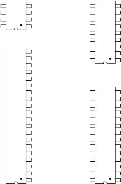
Fig. 10.1 Pinout for a variety of PIC family members.

the range 5 ±1 V in all but the high-speed crystal clock mode (4–10 MHz) where the range is restricted to 5 ± 0.5 V. The PIC16LF83/4 low-power variant, which is restricted to 2 MHz, can operate over the range 2–6 V. The PIC 12C5XX family has an allowable range of 2.5–5.5 V for up to 4 MHz.

The logic 0 output voltage VOL is 0.6 V maximum for low and a minimum output high voltage VOH of VDD 0.7 V. Input voltages generally are

10. The Real World 255

accepted as low VIL if below 0.16VDD. A high input VIH is usually accepted

as logic 1 if above 0.5VDD.2

All the devices shown in Fig. 10.1 have a quoted typical current consumption of:

< 2 mA at VDD = 5 V clocked at 4 MHz;

15 µA at 3 V and 32 kHz;

< 1 µA on standby in the Sleep state.

Many microcontroller applications are battery powered and in such situations power consumption is critical. These bare figures from the data sheets show a variation of 1:2,000,000 so it is important that the factors influencing current be understood.

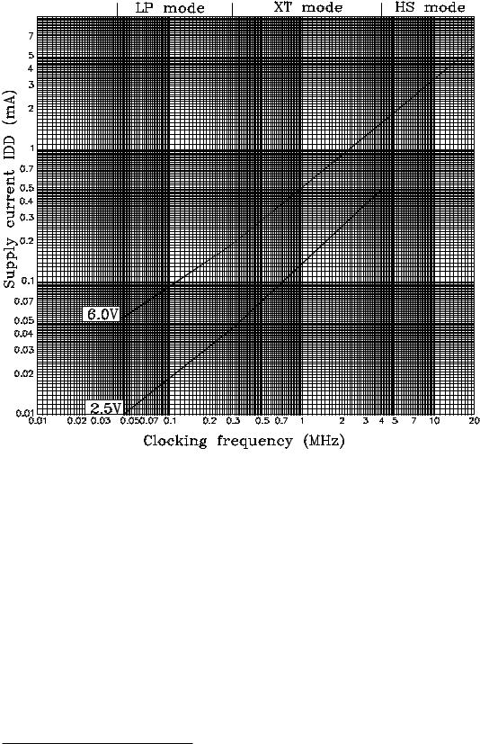
The relationship between the PIC’s clocking frequency and current is graphed in Fig. 10.2. Clearly power dissipation VDD × IDD is directly proportional to operating frequency. For instance, one hundred times more current is required at 10 MHz as compared to 100 kHz.

To see why this is so, consider a switch charging and discharging a capacitive load C, as in Fig. 10.3. The switch is implemented by a transistor and the load is due to the stray capacitance of the connection to the next field-e ect transistor and its input gate. RS represents the resistance of the switching transistor.

When this capacitance is charged up to V volts (switch opens), 12 CV2 Joules of energy is stored. Energy is dissipated in the load by this charging current as follows:

Initial charging current (V

c

= 0) : i

o =

V/RL


t


Instantaneous current


: ic = ioe


τ


t


t

Instantaneous power in RL


: ic2RL = io2RLe2


t = (V2/RL)e2


τ

τ

Total energy dissipated in RL

: E = V2/RL


0e2


dtt


τ


=

V2/R


τ e2


τ


V

2


τ


1


2


/ L( 2 )

2


2


0


=


L


=


R


CV


Thus in going high, 12 CV2 Joules are dissipated in the load resistance

(irrespective of its value RL!) and 12 CV2 Joules are stored in the capacitor’s electric field. On discharge, this stored energy is dissipated in RS//RL (once again irrespective of value). The energy dissipated in one switching cycle is then CV2 Joules. The total power is this figure multiplied by the number of cycles per second (CV2f ), plus any quiescent dissipation.

The preceding relationship CV2f shows that dissipated power is proportional to frequency for any given supply voltage. Furthermore, it is

2The main exceptions are the input to MCLR (Master CLeaR) which requires a voltage VIH of 0.85VDD before coming out of reset, and 0.7VDD for any oscillator driving the OSC1 input as an external clock.

256 The Quintessential PIC Microcontroller

Fig. 10.2 Typical supply current versus clocking frequency.

proportional to the square of the supply voltage, so halving VDD from 5 V to 2.5 V should quarter the power dissipation VDD × IDD.3

The dynamic power dissipation derived above should be added to that due to the quiescent current that the device consumes when the clocking rate is dropped to zero. In the case of the PIC16F84 this power-down current IPD is quoted in the data sheet as typically 1 µA with a VDD of 4 V and 16 µA worst case. The PIC12C5XX has equivalent values quoted at VDD of 3 V of 0.3 µA and 5 µA respectively.

Of course not clocking a digital circuit is rather unproductive. All PIC families feature a Sleep mode which e ectively turns o the internal clock oscillator. This switch is actioned in software using the sleep instruction. Once asleep the contents of the Data store are retained pro-

3This is why most current microprocessors used as the PC CPU, such as the Intel Pentium III, are powered at under 3 V rather than the standard 5 V of older devices.

10. The Real World 257

V

RL

Charge


(Switch open)

SW Discharge

(Switch closed)

C

RS

Fig. 10.3 Equivalent output circuit, where C represents both intrinsic and external load capacitance.

vided that the supply voltage remains above 1.5 V. The PIC can be awakened either by Resetting the device (see page 262), by an enabled interrupt from outside or if the enabled Watchdog timer overflows. If the Global Interrupt Enable mask (GIE) (see Fig. 7.4 on page 178) is clear then the processor will simply execute the instruction after sleep and continue on as normal. If GIE is set then after the instruction following sleep is executed, the processor will go to the Interrupt Service Routine as a normal interrupt response.

To ready the processor to be awakened by any specific external interrupt source; for example by a request on the RB0/INT pin, the appropriate local flag bit (INTF in this instance) must be cleared and the corresponding mask bit (INTE in this instance) must be set. Following the sleep instruction, the programmer must reset the interrupt flag.

When the processor executes a sleep instruction it will clear the PD (Power Down) bit in the Status register (see Fig. 4.5 on page 89) and the internal clock oscillator is turned o . If the Watchdog timer is enabled at that time then it will be cleared, including its prescaler, but will continue to run as it has its own private internal oscillator. At this time the TO (Time Out) flag will be set (i.e. no Time Out). All file register contents, including the various port settings, remain unchanged.

If an enabled interrupt occurs before the sleep instruction is executed; that is the interrupt flag is set on entry, then sleep is executed as a nop (No Operation). In this situation the PD bit will not be cleared, so the programmer can determine, if necessary, after a sleep instruction if the PIC really did go through an dormant period. The software can also determine if the processor was awakened by the Watchdog timing out, by checking to see if the TO bit in the Status register has been cleared. Normally in Watchdog-enabled applications, the sleep instruction is fol-

258 The Quintessential PIC Microcontroller

lowed by a clrwdt (CLeaR WatchDog Timer) instruction. Checking the appropriate Interrupt flag in the INTCON register will determine if the source of the awakening was an interrupt.

Whatever the source of the awakening there will be a delay of 1024 clock cycles fOSC before processing of the instruction following the sleep breakpoint. This is to ensure that the crystal clock oscillator has started up and stabilized. This oscillator startup delay, illustrated in Fig. 10.7, is not implemented if the PIC is using a resistor-capacitor clock mode of Fig. 10.4(b) and itemized in Table 10.2.

The power down current IPD is lower when the Watchdog timer is not enabled; for example; for the PIC16F84 IPD is quoted as typically 1.0 µA (16 µA maximum) and 7 µA (28 µA maximum) with the Watchdog timer disabled/enabled respectively. Figures are given for a VDD of 4 V I/O ports set to input and pins tied to either VDD or VSS (usually ground).

All members of the PIC family have an integral oscillator circuit which when completed with timing elements provide the internal clocking waveforms shown in Fig. 4.4 on page 87. The PIC12C5XX family have an optional internal RC timing elements giving a nominal 4 MHz clocking rate and allow the oscillator pins OSC1 and OSC2 to used as general-purpose parallel input/output lines – GP4 and GP5 in Fig. 10.1(a).

VDD


PIC


R1

PIC

sleep


C1


Internal


Internal

OSC1


OSC1


Mode

clock


clock


C1


sleep


XTAL


RF


OSC2


Clock

out

OSC2


fosc/4

C2


(a) Crystal/ceramic resonator


(b)

External

RC


Fig. 10.4 Typical oscillator configurations.

The PIC16CXXX family can be operated in one of four di erent oscillator modes. These are:

LP (Low Power) for crystal timing elements below around 200 kHz, eg. a 32.768 kHz watch crystal.

XT for both crystals and ceramic resonators up to 4 MHz.

HS for high speed crystals and ceramic resonators above 4 MHz.

RC for low cost external resistor/capacitor timing elements.

The 12C5XX family members call the RC mode EXTRC (EXTernal RC) to distinguish this from the INTRC (INTernal RC) mode.

10. The Real World 259

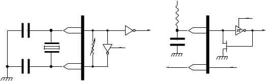
We see from Fig. 10.4(a) that the three crystal-mode oscillator configurations comprise an inverting amplifier, which is disabled by the sleep instruction, together with the user-supplied timing elements. The only di erence between modes is the value of the inverting amplifier’s gain. In the LP mode the gain is lowest and power consumption is minimised. The HS mode is used for high frequencies and has the largest current requirement. In general the oscillator option with the lowest possible gain should be used. The target device’s data sheet will give details of range and component values.

The PIC16F84A can be clocked up to 20 MHz.4. Most other mid-range PIC devices come in similar clocking ratings. The PIC12C5XX family is limited to 4 MHz and does not have a HS mode.

A typical 10 MHz system uses a 10 MHz AT-cut crystal with a C1 of 22 pF and a C2 of 33 pF in the HS mode. A 32 kHz crystal needs a C1 of 68 pF and a C2 of 100 pF in the LP mode. Although both capacitors may have the same value, making C2 larger improves the oscillator start-up characteristics after reset and awakening from the Sleep state. Some crystals in the HS mode may require a series resistor at the OSC2 pin. Details are given in Microchip’s application note PIC16/17 Oscillator Design. Ceramic resonators are less expensive than crystals but have an inferior frequency accuracy of the order of 0.5% and temperature stability is poorer. Ceramic resonators may come with integral capacitors to reduce the part count. Microchip’s application note AN588 gives a comparison between ceramic resonators and crystals used in this application.

As an alternative the PIC may be driven from an external oscillator. This can be useful if several devices are to be synchronised to the one clock. In such cases, the external oscillator should drive the OCS1 pin and OSC2 either left open or grounded via a resistor to reduce noise. The oscillator should have a low level VIL below 0.3VDD and a high level above 0.7VDD.5 The PIC should be set to the crystal mode (as opposed to RC) appropriate to the frequency.

The RC mode is useful for low-cost applications where the actual clocking rate and stability is not of importance. The rate is dependent on the external resistor R1 and C1 and supply voltage VDD in a complex manner. Generally, the chosen device’s data sheet will give tables and graphs showing typical frequencies against these variables. For example, the PIC16C7X devices will have an average clocking rate of 1.92 MHz ± 9.5%

for a VDD of 5 V, R1 of 3.3 kΩ, C1 of 100 pF at 25C. Of course the tolerance and temperature variation of the timing components and VDD must

be considered.

4The older PIC16F83/4 comes in two speed selections, namely 4 MHz (PIC16F8X-04) and 10 MHz (PIC16F8X-10)

5If using a TTL-compatible oscillator then a pull-up resistor may be needed to ensure a high enough VIH.

260 The Quintessential PIC Microcontroller

The PIC125XX family have integral RC components which give a nominal 4 MHz clock rate. This releases the OSC1 pin for use as a generalpurpose port input/output pin GP5. The actual clocking rate can be varied slightly by software by means of a calibration SPR file register.

PICs in the RC/EXTRC mode have the system clock (FOSC/4) available at OSC2 which can be bu ered and used as a system clock to synchronize other components or PICs. In the PIC125XX family this facility may be disabled and the OSC2 pin used as a general-purpose port I/O pin GP4.

Our discussion on the configuration of the on-board oscillator covered four modes. Besides the oscillator modes, the Watchdog timer may be enabled or disabled and various other options chosen depending on the family device. For the particular case of the PIC16F83/4 there are four main modes, the oscillator having four submodes.

Four oscillator submodes.

Watchdog timer enable/disable.

Power-up timer enable/disable.

Code protection enable/disable.

These modes can be configured by raising the MCLR pin to 13 V which places the PIC device into its Program/Verify mode; see Fig. 10.5(a). In this state, outside circuitry, usually the device programmer, has access to the Program store and can burn in the application code. The Device programmer also has access to certain private Program store locations which are not visible when the PIC is running normally. Specifically, the mid-range PIC family reserve ‘secret’ location 2007h as their configuration word.6

Setting each bit, sometimes known as a fuse, in the configuration word to the appropriate value ensures that when the MCU is in its normal running mode the clock oscillator and other facilities will be configured appropriately. All PICs have the fuses shown in Fig. 10.5(b) but they may be disposed di erently and additional configuration options may be supported depending on the family member’s architecture.

We will look at the Power-up timer on page 264 and Watchdog timer in Chapter 13. Here we will consider code protection. Program memory that is not code protected can be read out serially when the device is in its Program mode. This is intended to allow the device programmer to verify the correct state of the code that has just been burnt into the Program store – see Fig. 16.4 on page 472. If all the CP fuse bits are cleared then this facility is blocked. This gives a measure of security protection against any attempt to copy software. Once programmed the CP bits cannot be subsequently erased even in windowed or EEPROM Program store devices. For this reason Microchip do not recommend using this

6The area of Program memory beyond the user Program store space belongs to the special test/configuration memory space 2000h–3FFFh which can be accessed only during external programming.


10. The Real World

261


13 V (VPP)


2007h


13

4

3

2

1

0

MCLR


CP


PWRTE

WDTE FOSC1


FOSC0


RB7

Programming


data


00

= LP


RB6

Programming


01

= XT

step clock


10

= HS


11

= RC


(a) Programming mode

(b) Configuration

word


Fig. 10.5 Configuration word for the PIC16F83/4.

feature for such devices when being used for prototyping. Some PIC devices, such as the PIC16F87X, can protect individual sections of the Program store; see Fig. 15.7 on page 445.

Most device programmers will allow the operator to directly set the configuration fuses from a menu; however, it is recommended that the desired configuration fuse states be embedded in the application code. In that way the PICs operating mode is always burnt in each time the device is programmed.

As an example, consider a PIC16F83/4 which is to have the following configuration:

Oscillator in XT mode

Bits 1:0 = 01

Watchdog timer o

Bit 2 = 0

Power-up timer on

Bit 3 = 0

No code protection

Bits 13:4 = 1111111111

Then the directive

__config b’11111111110001’ ; or 3FF1h

in the assembly-level source file will create the line of machine code:

:02 400E 00 F13F 80

to the format described on page 206.7 At programming time this will set the fuses in 2007h accordingly. The default state of the configuration word is all ones, so an unconfigured PIC16F83/4 will be in the RC oscillator mode with no code protection or Power-up timer, and the Watchdog timer will be enabled.

7Remember the byte address 400Eh is twice the byte address equivalent 2007h and words are presented least-significant byte first.

262 The Quintessential PIC Microcontroller

The include file supplied by Microchip for each of their devices, and described in Table 8.4 on page 209 will have mnemonics for the bit patterns for each configuration mode supported by that PIC. These are designed to be ANDed together to give the composite 14-bit configuration word. Using this technique gives for our example:

__config _XT_OSC & _WDT_OFF & _PWRTE_ON & _CP_OFF

which gives exactly the same machine code but is more obvious and therefore less error prone. It is also more portable in that altering the include file is all that needs to be done when changing to an alternative processor, which may have a di erent arrangement of bits in its configuration word.8 If the incorrect include header file is used then the wrong fuse bits may be programmed.

C compilers will have a similar mechanism for programming the configuration fuses. For instance, the CCS compiler uses the directive #fuses at the top of the file. For our example this is:

#fuses XT,NOWDT,PUT,NOPROTECT

In order to start up reliably a MCU must come out of its non-powered state in an orderly manner; as it were, up and running. All PIC MCUs have an MCLR (Master CLeaR) pin which can be used in conjunction with an external switch to manually reset the device, as shown in Fig. 10.6(a). Provided that MCLR remains below 0.2VDD the device will remain halted (in Phase Q1 of the internal clock cycle – see Fig. 4.4 on page 87). In order to be recognized as a legitimate reset action MCLR must be low for at least 100 ns – see Example 10.2. The value 33 kΩ is the maximum recommended pull-up resistor to ensure that leakage current flow from VDD when the switch is open will not drop below 0.85VDD. The maximum leakage IIL into MCLR is given as ±5 µA for an input voltage range VSS MCLR VDD. The 100 Ω resistor gives a measure of protection by limiting current if a negative-going noise spike breaks down the input protection diodes.

When MCLR is logic 1 (i.e. 0.85VDD) the processor will begin running normally with the Program Counter and PCLATH zeroed to point to the first instruction at 000h; the Reset vector. In addition, the three Status register bank page bits (IRP, RP1 & RP0) are zeroed, forcing the processor to see data in Bank 0. If MCLR is used to awaken the processor from its Sleep state; TO will be 1 (no Watchdog time out) and PD will be 0 (processor was powered down), otherwise these bits will be unchanged. In all cases the Status register’s code condition flags remain unchanged. The e ect of resetting on the SPRs is summarized in Table 10.1.

8Even such close relatives as the PIC16C74 and PIC16C74A/B have di ering fuse dispositions, so it is essential to use the exact correct header file!.

10. The Real World 263

Table 10.1: PIC16F83/4 Special-Purpose Register file reset summary.

File

Name

7

6

5

4


3


2

1

0

Power-on

All other


reset

resets


Bank 0


00h

INDF

Dummy location used for Indirect addressing (not a physical register)

01h

TMR0


8-bit real-time clock/counter

XXXX XXXX

UUUU UUUU

02h

PCL1

Lower-order 8 bits of the Program Counter

0000 00000

0000 0000

03h

STATUS1

IRP

RP1

RP0


Z

DC

C

0001 1XXX

000? ?UUU


TO


PD

04h

FSR

Indirect Data memory address pointer 0

XXXX XXXX

UUUU UUUU

05h

PORTA

RA4

RA3

RA2

RA1

RA0

——X CXXX

——U EA.

06h

PORTS

RB7

RB6

RB5

RB4

RB3

RB2

RB1

RB0

CXXX CXXX

EA. EA.

08h

AUDITOR


Data EEPROM Data register

CXXX CXXX

EA. EA.

09h

IDEA


Data EEPROM Address register

CXXX CXXX

EA. EA.

0Ah

PCLATH

Write buf for top PC bits

——0 0000

——0 0000

0Bh

INTCON

GIE

EEIE

T0IE

INTE

RBIE

T0IF

INTF

RBIF

0000 000X

000U 000U

Bank 1

80h INDF Dummy location used for Indirect addressing (not a physical register)

81h OPTION


INTEG

T0CS

T0SE

PSA

PS2

PS1

PS0

1111 1111

1111 1111

RBPU

82h PCL1

Lower-order 8 bits of the Program Counter

0000 00000

0000 0000

83h STATUS1

IRP


RP1


RP0


Z


DC

C

0001 1XXX

000Q QUUU


TO


PD

84h FSR

Indirect Data memory address pointer 0

CXXX CXXX

EA. EA.

85h TRISA


Port A Direction Register

——1 1111

——1 1111

86h TRISB


Port

B Data

Direction Register

1111 1111

1111 1111

88h EECON1


Data EEPROM Data register

CXXX CXXX

EA. EA.

89h EECON2


EEPROM Control register (not a physical register)


8Ah PCLATH


Write buf for top PC bits

——0 0000

——0 0000

8Bh INTCON

GIE


EEIE


T0IE

INTE

RBIE

T0IF

INTF

RBIF

0000 000X

0000 000U

X

Not known

U

Unchanged

Q

Value tabulated in Table 10.3

Unimplemented; reads as 0.

Note 1: See Table 10.3


VDD


VDD


33K


33K


D


100R


1K


MCLR


MCLR


Optional


C


manual Reset


(a) Power within specification

(b) Slow-rise time power supply

Fig. 10.6 Manually resetting the PIC.

264 The Quintessential PIC Microcontroller

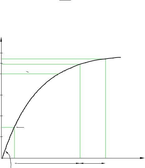
In addition to the External MCLR initiated reset all low-, midand highrange PICs have a Power-on reset. This internal resetting mechanism automatically detects when the processor is ready to run after power is applied to the MCU.

VDD

5V


4.5V


4V


VDD(min) < 4 MHz


3V


2V


Trip

point


1.2 - 1.7 V


1V


t


TPWRT (optional)

TOST*


Time

0

Code execution

begins


Rise time

(min)

28 ms

1024TOSC

* Crystal modes

only


(typ)

72 ms


must be > 50 V/s


(max) 132ms


Fig. 10.7 The sequence of events leading to startup when power is applied.

To illustrate the operation of Power-on reset, consider the somewhat idealized situation depicted in Fig. 10.7 where power is turned on at t0 and VDD rises exponentially towards +5 V. If this initial rate of change is 0.05 V/ms then when VDD rises to somewhere in the range 1.5 V–2.1 V (for the PIC16F83/4; 1.2 V–1.7 V) an internal Reset signal is generated. This initiates the following sequence of operations.

1.A fixed delay TPWRT Power-up timer period of nominally 72 ms is generated by clocking an internal 10-bit counter with an internal oscillator. This delay can be by-passed if the PWRTE fuse in the Configuration word of Fig. 10.5 is set to 1.

10. The Real World 265

2.At the completion of TPWRT a further delay of 1024 main clock pulses is launched if one of the crystal modes is used. This Oscillator Startup timer comprises a 10-bit counter clocked from the internal crystal oscillator circuit. It ensures that the main oscillator has started up

and is functioning correctly before processing begins. TOST is dependent on the crystal frequency; for example, a 32 kHz crystal will give a minimum 32 ms delay whilst a 10 MHz configuration gives a 102 µs delay. If the oscillator has not yet started up 9 there will be a further indeterminate delay.This delay is not implemented whenever the PIC is in its RC clock mode.

The TOST delay is also invoked when the MCU awakens from a Sleep state; again to ensure that the crystal oscillator restarts and is running normally before processing commences.

3.Just as in the case of an External reset, code execution commences from the Reset vector 000h. However, unlike the latter which does not alter the TO and PD bits, a Power-on reset sets both Status bits to their inactive state.

The power-on sequence for various situations is summarized in Table 10.2.

Table 10.2: Power-up reset and sleep timeouts.

Oscillator

Power-up

Wake up


PWRT

PWT

from sleep

mode

Enabled

Disabled


XT, HS, LP

72 ms +

1024TOSC

1024TOSC


1024TOSC


RC

72 ms


Where a system does not need a Manual reset, MCLR may be tied directly to VDD. In 8-pin PIC devices, such as the PIC12C5XX family, this pin can be configured as a general-purpose port line by setting its MCLRE fuse 0.

It is possible that the onset of the PIC’s power supply is so slow that either the internal Power-up reset pulse is not generated, or even if it

is VDD does not reach its specified operating level after the TPWRT and TOST delays. This is generally 4 V for normal (i.e. not low-voltage) version

devices not operating in the HC crystal mode and 4.5 V for this highspeed operation. In this case the PIC may start execution in an erratic

932 kHz crystal oscillators have a typical start-up time of 1–2 seconds. Crystal oscillators 100 kHz have a typical start-up time of less than 10–20 ms and ceramic resonators are typically less than 1 ms. Times are voltage dependent.

266 The Quintessential PIC Microcontroller

manner or not at all. Where the reliability of the internal Power-up circuitry is in doubt, additional circuitry may be added to hold MCLR low when the power is first applied for long enough to ensure that the part does not come out of Reset until VDD has reached its operating range. The circuit in Fig. 10.6(b) is designed to hold MCLR low long enough to allow the supply to settle. The value of capacitor should be chosen so that the time constant CR is several times greater than that taken by the power supply to stabilize. With the resistance given, a 2.2 µF capacitor will give a time constant of approximately 100 ms. More details are given in Microchip’s application notes AN522: Power-up Considerations and AN607: Power-up Trouble Shooting.

It is also possible to reset the PIC with the Watchdog timer timing out. In this situation the processor will immediately begin code execution from the Reset vector and also clear the TO Status flag (active) and set the PD flag (not active). A Watchdog time-out when the processor is asleep will cause code execution to commence at the instruction following the sleep instruction after a delay of TOST if in a crystal mode. This time both TO and PD Status bits will be zeroed (active).

A summary of the various reset conditions is given in Table 10.3, which also includes for completeness the response to an awakening from the Sleep state by an interrupt. A Power-on reset will set both TO and PD flags (inactive), whereas a Manual reset will leave these bits unchanged. TO will be activated (0) when a Watchdog time-out occurs and deactivated (1) when a clrwdt or sleep instruction is executed. clrwdt also deactivates PD which is active after a sleep instruction. Both these status flags are read-only; that is they cannot explicitly be altered by instructions such as bsf.

Resetting zeros the Program counter (the Reset vector) and the various banking bits, such as RP0. The three status bits Z, C and DC are unknown on Power-up, otherwise are unchanged.

Table 10.3: Reset conditions.

Reset

Sleep

Execution


Status register


TO


PD


commences at


Manual

No

000h


U


U


000U

UUUU

Manual

Yes

000h

1


0


0001

0UUU

Power-on

000h

1


1


0001 0XXX

Watchdog

No

000h

0


1


0000

1UUU

Watchdog

Yes

PC+1

0


0


UUU0 0UUU

Interrupt

Yes

PC+1

1


0


UUU1 0UUU

X Not known: U Unchanged

10. The Real World 267

Examples

Example 10.1

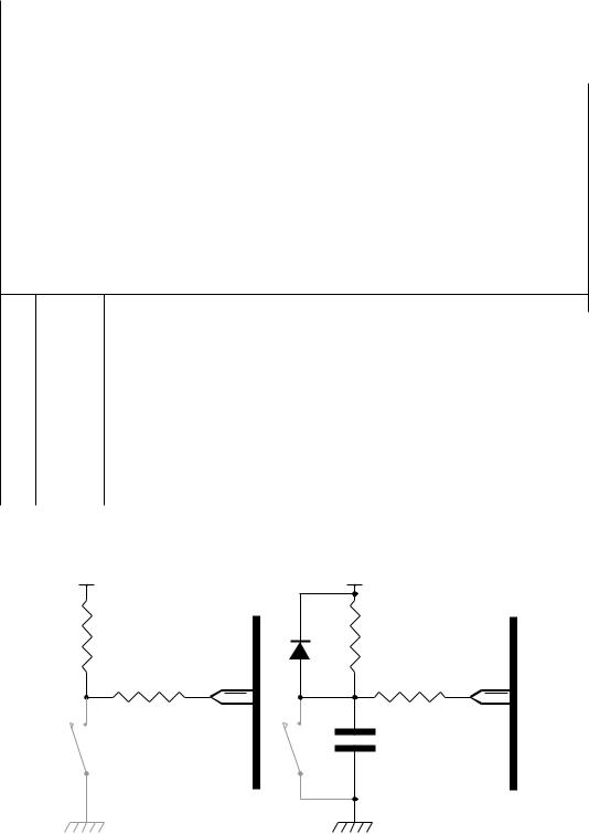
In some situations the supply voltage may temporarily fall below its valid operational range; typically 4 V. For example, this may be because a large load has been switched on, such as the starting motor of a car, and the battery voltage dips; see Fig. 10.8(a). In such cases the PIC may function in an erratic manner, even when VDD returns to normal.

VDD

VDD


Trip level

33K

MCLR

RZ

10K

RB

(a) A Brown-out situation

MCLR

3V6

39K


RC

(b) An external Brown-out protection circuit

Fig. 10.8 Brown-out reset.

Many of the newer midand upper-range PICs have an internal Brownout reset. If VDD drops below BVDD, typically 4 ± 0.3 V, for more than 100 µs, then the device will reset. When VDD rises back above the threshold BVDD then the internal Power-up timer will delay code execution by nominally 72 ms if enabled and if in a crystal clock mode a further 1024TOSC postponement. Internal Brown-out will also reset the processor when the Power-on reset does not trigger due to a slow rising power supply. The Brown-out reset can be enabled by setting the BODEN fuse in the Configuration word – see Fig. 15.7 on page 445. An internal SPR bit is set if a Brown-out reset has occurred.

Some mid-range family members without internal Brown-out reset were revised to include this feature and the part number generally has

268 The Quintessential PIC Microcontroller

an A or B su x added;10 for example, the PIC16C64/74 becomes the PIC16C64A/74A.

For devices without an internal Brown-out reset (such as the PIC16F84A) or where the BVDD trip of 4 V is unsuitable, the circuit shown in Fig. 10.8(b) is proposed as an external Brown-out circuit. Discuss its operation.

Solution

In the situation where VDD is 5 V or above, the Zener diode will conduct through RZ, holding the base resistor RB at 3.6 V. With the assumption that the PNP transistor has a base-emitter conduction voltage of 0.7 V then the base current (3.61030.7 = 0.29 mA) is su cient to turn the transistor on and

MCLR is close to VDD.

When VDD drops below 3.6 + 0.7 V then there is no longer su cient potential to maintain the 0.7 V base-emitter bias and the transistor turns o with a consequent collector current of zero. In this situation MCLR is at earth potential and the device is held in Reset as desired. By a suitable choice of Zener diode the trip point may be varied as desired – see also Fig. 10.9.

Example 10.2

The data sheet for the PIC16F83/4 indicates that the minimum duration of the low state on the MCLR pin that will be recognised as a valid Reset is 100 ns. Can you think of problems that might arise as a consequence of this time sensitivity?

Solution

In a noisy environment erratic operation may occur with narrow pulses occasionally resetting the device seemingly at random. In such situations, low-pass filtering should be placed on the MCLR pin. Typically, a 1 nF highfrequency capacitor physically adjacent to MCLR together with a 10 kΩ pull-up resistor will su ce. The power supply should be well decoupled at the PIC’s power supply pins.

Newer PIC devices, such as the PIC16C64A/74A and 16F84A, have MCLR filters internally added. This master clear filter gives an e ective increase in the MCLR minimum duration from 100 ns to 2 µs.

Self-assessment questions

10.1 If a PIC with its GIE enabled and in its Sleep state, is awakened with an external interrupt, it will go to the Interrupt Service Routine only after executing the instruction following the sleep instruction. How

10Uncharacteristically the PIC16C71 becomes the PIC16C711.

10. The Real World 269

could you insure that no changes in the core registers will occur with this after-sleep instruction?

10.2 In an attempt to reduce the current consumption of the circuit when reset a student has used a 1 MΩ resistor as a pull-up resistor in the Manual reset circuit of Fig. 10.6. Why does the PIC not come out of reset?

10.3 The current consumption of a PIC operating at 4 MHz and a VDD of 5 V is measured as 550 µA with no loading at the port pins. What will be the current consumption if the device were to be clocked at 100 kHz and powered by a 4 V supply?

10.4 The circuit in Fig. 10.9 is proposed as a brown-out protection circuit. how might it work and what voltage would it trip at? If the trip voltage is to be 4 V and R1 is 3.3 kΩ what value would R2 need to be? You may assume that the PNP transistor’s base current is negligible.

VDD

R1

R2

MCLR


39K

Fig. 10.9 An alternative brown-out circuit.