

Furber S.ARM system-on-chip architecture.2000
.pdf5-stage pipeline ARM organization |
79 |
Memory bottleneck
The 5-stage pipeline
with a given compiler using a given set of optimizations, and so on) there are only two ways to increase performance:
•Increase the clock rate, fclk.
This requires the logic in each pipeline stage to be simplified and, therefore, the number of pipeline stages to be increased.
•Reduce the average number of clock cycles per instruction, CPI.
This requires either that instructions which occupy more than one pipeline slot in a 3-stage pipeline ARM are re-implemented to occupy fewer slots, or that pipeline stalls caused by dependencies between instructions are reduced, or a combination of both.
The fundamental problem with reducing the CPI relative to a 3-stage core is related to the von Neumann bottleneck - any stored-program computer with a single instruction and data memory will have its performance limited by the available memory bandwidth. A 3-stage ARM core accesses memory on (almost) every clock cycle either to fetch an instruction or to transfer data. Simply tightening up on the few cycles where the memory is not used will yield only a small performance gain. To get a significantly better CPI the memory system must deliver more than one value in each clock cycle either by delivering more than 32 bits per cycle from a single memory or by having separate memories for instruction and data accesses.
As a result of the above issues, higher performance ARM cores employ a 5-stage pipeline and have separate instruction and data memories. Breaking instruction execution down into five components rather than three reduces the maximum work which must be completed in a clock cycle, and hence allows a higher clock frequency to be used (provided that other system components, and particularly the instruction memory, are also redesigned to operate at this higher clock rate). The separate instruction and data memories (which may be separate caches connected to a unified instruction and data main memory) allow a significant reduction in the core's CPI.
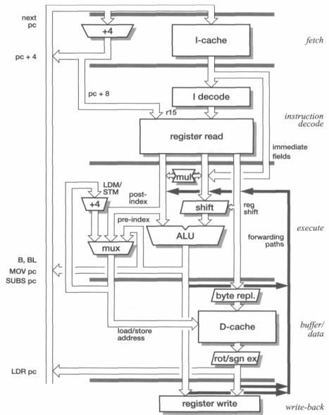
A typical 5-stage ARM pipeline is that employed in the ARM9TDMI. The organization of the ARM9TDMI is illustrated in Figure 4.4 on page 81.
The ARM processors which use a 5-stage pipeline have the following pipeline stages:
•Fetch;
the instruction is fetched from memory and placed in the instruction pipeline.
•Decode;
the instruction is decoded and register operands read from the register file. There are three operand read ports in the register file, so most ARM instructions can source all their operands in one cycle.
80 |
ARM Organization and Implementation |
•Execute;
an operand is shifted and the ALU result generated. If the instruction is a load or store the memory address is computed in the ALU.
•Buffer/data;
data memory is accessed if required. Otherwise the ALU result is simply buffered for one clock cycle to give the same pipeline flow for all instructions.
•Write-back;
the results generated by the instruction are written back to the register file, including any data loaded from memory.
This 5-stage pipeline has been used for many RISC processors and is considered to be the 'classic' way to design such a processor. Although the ARM instruction set was not designed with such a pipeline in mind, it maps onto it relatively simply. The principal concessions to the ARM instruction set architecture in the organization shown in Figure 4.4 on page 81 are the three source operand read ports and two write ports in the register file (where a 'classic' RISC has two read ports and one write port), and the inclusion of address incrementing hardware in the execute stage to support load and store multiple instructions.
Data forwarding A major source of complexity in the 5-stage pipeline (compared to the 3-stage pipeline) is that, because instruction execution is spread across three pipeline stages, the only way to resolve data dependencies without stalling the pipeline is to introduce forwarding paths.
Data dependencies arise when an instruction needs to use the result of one of its predecessors before that result has returned to the register file. (This issue was discussed previously under 'Pipeline hazards' on page 22.) Forwarding paths allow results to be passed between stages as soon as they are available, and the 5-stage ARM pipeline requires each of the three source operands to be forwarded from any of three intermediate result registers as shown in Figure 4.4 on page 81.
There is one case where, even with forwarding, it is not possible to avoid a pipeline stall. Consider the following code sequence:
LDR |
rN, [ . . ] |
; load |
rN from somewhere |
ADD |
r2, r1, rN |
; and use |
it immediately |
The processor cannot avoid a one-cycle stall as the value loaded into rN only enters the processor at the end of the buffer/data stage and it is needed by the following instruction at the start of the execute stage. The only way to avoid this stall is to encourage the compiler (or assembly language programmer) not to put a dependent instruction immediately after a load instruction.
Since the 3-stage pipeline ARM cores are not adversely affected by this code sequence, existing ARM programs will often use it. Such programs will run correctly
5-stage pipeline ARM organization |
81 |
|
Figure 4.4 ARM9TDMI 5-stage pipeline organization. |
|
on 5-stage ARM cores, but could probably be rewritten to run faster by simply reor- |
|
dering the instructions to remove these dependencies. |
PC generation |
The behaviour of r15, as seen by the programmer and described in 'PC behaviour' |
|
on page 78, is based on the operational characteristics of the 3-stage ARM pipeline. |
|
The 5-stage pipeline reads the instruction operands one stage earlier in the pipeline, |
|
and would naturally get a different value (PC+4 rather than PC+8). As this would |
82 |
ARM Organization and Implementation |
lead to unacceptable code incompatibilities, however, the 5-stage pipeline ARMs all 'emulate' the behaviour of the older 3-stage designs. Referring to Figure 4.4, the incremented PC value from the fetch stage is fed directly to the register file in the decode stage, bypassing the pipeline register between the two stages. PC+4 for the next instruction is equal to PC+8 for the current instruction, so the correct r15 value is obtained without additional hardware.
4.3ARM instruction execution
Data processing instructions
Data transfer instructions
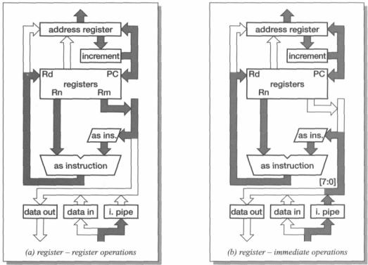
The execution of an ARM instruction can best be understood by reference to the datapath organization as presented in Figure 4.1 on page 76. We will use an annotated version of this diagram, omitting the control logic section, and highlighting the active buses to show the movement of operands around the various units in the processor. We start with a simple data processing instruction.
A data processing instruction requires two operands, one of which is always a register and the other is either a second register or an immediate value. The second operand is passed through the barrel shifter where it is subject to a general shift operation, then it is combined with the first operand in the ALU using a general ALU operation. Finally, the result from the ALU is written back into the destination register (and the condition code register may be updated).
All these operations take place in a single clock cycle as shown in Figure 4.5 on page 83. Note also how the PC value in the address register is incremented and copied back into both the address register and r15 in the register bank, and the next instruction but one is loaded into the bottom of the instruction pipeline (i. pipe). The immediate value, when required, is extracted from the current instruction at the top of the instruction pipeline. For data processing instructions only the bottom eight bits (bits [7:0]) of the instruction are used in the immediate value.
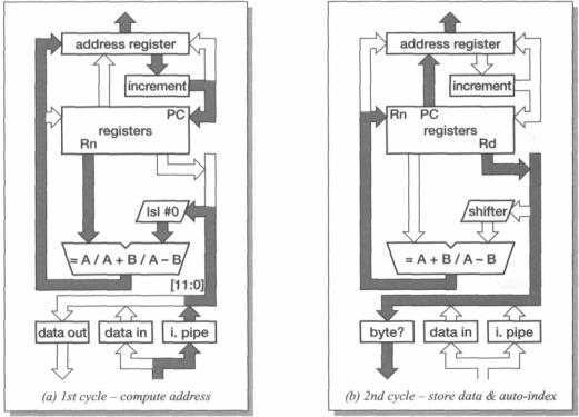
A data transfer (load or store) instruction computes a memory address in a manner very similar to the way a data processing instruction computes its result. A register is used as the base address, to which is added (or from which is subtracted) an offset which again may be another register or an immediate value. This time, however, a 12-bit immediate value is used without a shift operation rather than a shifted 8-bit value. The address is sent to the address register, and in a second cycle the data transfer takes place. Rather than leave the datapath largely idle during the data transfer cycle, the ALU holds the address components from the first cycle and is available to compute an auto-indexing modification to the base register if this is required. (If auto-indexing is not required the computed value is not written back to the base register in the second cycle.)
ARM instruction execution |
83 |
Figure 4.5 Data processing instruction datapath activity.
The datapath operation for the two cycles of a data store instruction (SIR) with an immediate offset are shown in Figure 4.6 on page 84. Note how the incremented PC value is stored in the register bank at the end of the first cycle so that the address register is free to accept the data transfer address for the second cycle, then at the end of the second cycle the PC is fed back to the address register to allow instruction prefetching to continue.
It should, perhaps, be noted at this stage that the value sent to the address register in a cycle is the value used for the memory access in the following cycle. The address register is, in effect, a pipeline register between the processor datapath and the external memory.
(The address register can produce the memory address for the next cycle a little before the end of the current cycle, moving responsibility for the pipeline delay out into the memory when this is desired. This can enable some memory devices to operate at higher performance, but this detail can be postponed for the time being. For now we will view the address register as a pipeline register to memory.)
84 |
ARM Organization and Implementation |
|
Figure 4.6 SIR (store register) datapath activity. |
|
When the instruction specifies the store of a byte data type, the 'data out' block |
|
extracts the bottom byte from the register and replicates it four times across the 32-bit |
|
data bus. External memory control logic can then use the bottom two bits of the |
|
address bus to activate the appropriate byte within the memory system. |
|
Load instructions follow a similar pattern except that the data from memory only |
|
gets as far as the 'data in' register on the second cycle and a third cycle is needed to |
|
transfer the data from there to the destination register. |
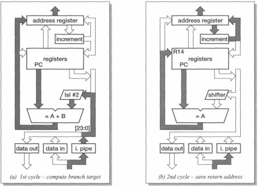
Branch |
Branch instructions compute the target address in the first cycle as shown in |
instructions |
Figure 4.7 on page 85. A 24-bit immediate field is extracted from the instruction and |
|
then shifted left two bit positions to give a word-aligned offset which is added to the |
|
PC. The result is issued as an instruction fetch address, and while the instruction |
|
pipeline refills the return address is copied into the link register (r14) if this is |
|
required (that is, if the instruction is a 'branch with link'). |
ARM instruction execution |
85 |
Figure 4.7 The first two (of three) cycles of a branch instruction.
The third cycle, which is required to complete the pipeline refilling, is also used to make a small correction to the value stored in the link register in order that it points directly at the instruction which follows the branch. This is necessary because r15 contains pc + 8 whereas the address of the next instruction is pc + 4 (see 'PC behaviour' on page 78).
Other ARM instructions operate in a similar manner to those described above. We will now move on to look in more detail at how the datapath carries out these operations.
86 |
ARM Organization and Implementation |
4.4ARM implementation
Clocking scheme
Datapath timing
The ARM implementation follows a similar approach to that outlined in Chapter 1 for MU0; the design is divided into a datapath section that is described in register transfer level (RTL) notation and a control section that is viewed as a finite state machine (FSM).
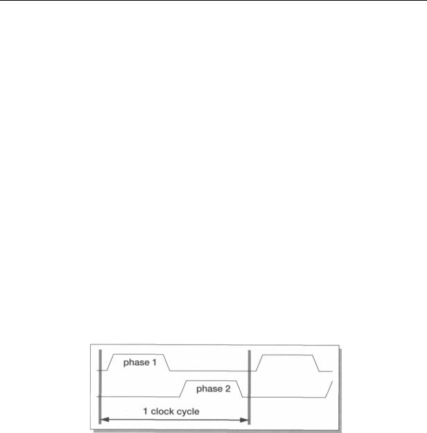
Unlike the MU0 example presented in Section 1.3 on page 7, most ARMs do not operate with edge-sensitive registers; instead the design is based around 2-phase non-overlapping clocks, as shown in Figure 4.8, which are generated internally from a single input clock signal. This scheme allows the use of level-sensitive transparent latches. Data movement is controlled by passing the data alternately through latches which are open during phase 1 and latches which are open during phase 2. The non-overlapping property of the phase 1 and phase 2 clocks ensures that there are no race conditions in the circuit.
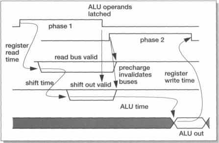
The normal timing of the datapath components in a 3-stage pipeline is illustrated in Figure 4.9 on page 87. The register read buses are dynamic and are precharged during phase 2 (here 'dynamic' means that they are sometimes undriven and retain their logic values as electrical charge; charge-retention circuits are used to give pseudo-static behaviour so that data is not lost if the clock is stopped at any point in its cycle). When phase 1 goes high, the selected registers discharge the read buses which become valid early in phase 1. One operand is passed through the barrel shifter, which also uses dynamic techniques, and the shifter output becomes valid a little later in phase 1.
The ALU has input latches which are open during phase 1, allowing the operands to begin combining in the ALU as soon as they are valid, but they close at the end of phase 1 so that the phase 2 precharge does not get through to the ALU. The ALU then continues to process the operands through phase 2, producing a valid output towards the end of the phase which is latched in the destination register at the end of phase 2.
Figure 4.8 2-phase non-overlapping clock scheme.
ARM implementation |
87 |
Figure 4.9 ARM datapath timing (3-stage pipeline).
Note how, though the data passes through the ALU input latches, these do not affect the datapath timing since they are open when valid data arrives. This property of transparent latches is exploited in many places in the design of the ARM to ensure that clocks do not slow critical signals.
The minimum datapath cycle time is therefore the sum of:
•the register read time;
•the shifter delay;
•the ALU delay;
•the register write set-up time;
•the phase 2 to phase 1 non-overlap time.
Of these, the ALU delay dominates. The ALU delay is highly variable, depending on the operation it is performing. Logical operations are relatively fast, since they involve no carry propagation. Arithmetic operations (addition, subtraction and comparisons) involve longer logic paths as the carry can propagate across the word width.
Adder design Since the 32-bit addition time has a significant effect on the datapath cycle time, and hence the maximum clock rate and the processor's performance, it has been the focus of considerable attention during the development of successive versions of the ARM processor.
88
ALU functions
The ARM6 carry-select adder
ARM Organization and Implementation
Figure 4.10 The original ARM1 ripple-carry adder circuit.
The first ARM processor prototype used a simple ripple-carry adder as shown in Figure 4.10. Using a CMOS AND-OR-INVERT gate for the carry logic and alternating AND/OR logic so that even bits use the circuit shown and odd bits use the dual circuit with inverted inputs and outputs and AND and OR gates swapped around, the worst-case carry path is 32 gates long.
In order to allow a higher clock rate, ARM2 used a 4-bit carry look-ahead scheme to reduce the worst-case carry path length. The circuit is shown in Figure 4.11 on page 89. The logic produces carry generate (G) and propagate (P) signals which control the 4-bit carry-out. The carry propagate path length is reduced to eight gate delays, again using merged AND-OR-INVERT gates and alternating AND/OR logic.
The ALU does not only add its two inputs. It must perform the full set of data operations defined by the instruction set, including address computations for memory transfers, branch calculations, bit-wise logical functions, and so on.
The full ARM2 ALU logic is illustrated in Figure 4.12 on page 89. The set of functions generated by this ALU and the associated values of the ALU function selects are listed in Table 4.1 on page 90.
A further improvement in the worst-case add time was introduced on the ARM6 by using a carry-select adder. This form of adder computes the sums of various fields of the word for a carry-in of both zero and one, and then the final result is selected by using the correct carry-in value to control a multiplexer. The overall scheme is illustrated in Figure 4.13 on page 90.