


VIA Eden ESP Processor Datasheet |
Preliminary Information |
January 2002
Thus, the VIA Eden ESP family architecture provides improved performance by optimizing MHz via a 12-stage pipeline while maintaining a good CPI. Complex CPI-driven features such as out- of-order instruction execution are not implemented because they (1) impact MHz, (2) require a lot of die area and power, and (3) have little impact on real performance since… (the next point)
!Memory performance is the limiting CPI performance factor. In modern PCs, the processor bus is slow compared to the internal clock frequency. Thus, off-chip memory-accesses dominate processor CPI as opposed to internal instruction execution performance.
The VIA Eden ESP processor addresses this phenomenon by providing many specific features designed to reduce bus activity: large primary caches, large TLBs, aggressive prefetching, an efficient level-2 cache (new to the VIA Eden ESP Samuel 2 and Ezra), and so forth.
!Different market segments have different workload characteristics. The hardware, operating systems, and applications used in fanless PC’s, internet appliances, small form factor PC’s have different technical characteristics than those in the high-end, workstation, or server market.
The VIA Eden ESP family exploits these differences by implementing very specific design tradeoffs, providing high performance with low cost in the target environments. These optimizations are based on extensive analysis of actual behavior of target-market hardware and software.
!Small is beautiful. VIA Eden ESP processors are highly optimized for small die size. In addition to the obvious cost benefits, this small size reduces power consumption and improves reliability.
2.2COMPONENT SUMMARY
2.2.1 GENERAL ARCHITECTURE & FEATURES
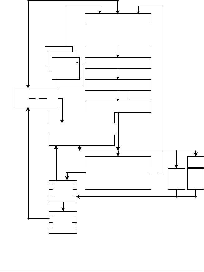
Figure 2-1 illustrates the basic 12-stage (integer) pipeline structure of the VIA Eden ESP family. At a high level, there are four major functional groups: I-fetch, decode and translate, execution, and data cache.
The I-fetch components deliver x86 instruction bytes from the large I-cache or the external bus. Large buffers allow fetching to proceed asynchronously to other operations. The decode and translate components convert x86 instruction bytes into internal execution forms. Branches are also identified, predicted, and the targets prefetched. Large buffers allow decoding and translating to proceed asynchronously to other operations. The execution components issue, execute, and retire internal instructions. The data cache components manage the efficient loading and storing of execution data to and from the caches, bus, and internal components.
At one level the VIA Eden ESP processor architecture seems simple: instructions are issued, executed, and retired in order, only one instruction can be issued per clock, and most data cache misses stall the pipeline. However, the design is actually highly optimized and highly tuned to achieve high performance in the targeted environment. Some of the significant features providing this performance are:
!High internal clock frequency. The 12-stage pipeline facilitates high MHz
!Large on-chip caches and TLBs. The VIA Eden ESP implements large caches and TLBs that significantly reduce stalls due to bus traffic. These primary caches and TLBs are larger than those on any other x86 processor:
•Two 64-KB primary (L1) caches with 4-way associativity
•A 4-way 64-KB unified level-2 (L2) cache
•Two 128-entry TLBs with 8-way associativity
2-2 |
Architecture |
Section 2 |
Preliminary Information |
VIA Eden ESP Processor Datasheet |
January 2002
•Two 8-entry page directory caches that effectively eliminate loads of page directory entries upon TLB misses
•A four-entry (8 bytes each) store queue that also forwards store data to subsequent loads
•A four-entry write buffer that also performs write combining
!Extensive features to further minimize bus stalls. These include:
•Full memory type range registers (MTRRs)
•A non-stalling write-allocate implementation
•Implementation of the “cache lock” feature
•Non-blocking out-of-order retirement of pipeline stores
•Implementation of x86 prefetch instruction (3DNow!)
•Implicit speculative data prefetch into D-cache
•Aggressive implicit instruction prefetch into I-cache
•Highly asynchronous execution with extensive queuing to allow fetching, decoding and translating, executing, and data movement to proceed in parallel
!High-performance bus implementation. The VIA Eden ESP socket 370 compatible bus implementation includes the following performance enhancements:
•No stalls on snoops
•Up to 8 transactions can be initiated by the processor
•Aggressive write pipelining
•Smart bus allocation prioritization
•100MHz and 133MHz bus operation
!Good performance for highly used instructions. Heavily used instructions—including complex functions such as protect-mode segment-register loads and string instructions—are executed fast. In particular, the pipeline is arranged to provide one-clock execution of the heavily used register– memory and memory–register forms of x86 instructions. Many instructions require fewer pipeline clocks than on comparable processors.
Section 2 |
Architecture |
2-3 |
VIA Eden ESP Processor Datasheet |
Preliminary Information |
January 2002
Socket
370 Bus
Bus Unit
|
|
I-Cache |
& |
I-TLB |
I |
|
|
|
|
|
|
|
|||
|
|
64 KB 4-way |
128-ent 8-way |
B |
I-Fetch |
|
|
|
|
8-ent PDC |
|
|
|||
|
|
|
|
|
|
||
|
|
predecode |
|
V |
|
|
|
|
|
|
|
|
|
||
Return stack |
decode buffer |
|
|
|
|
|
|
3 BHTs |
|
|
|
|
|
||
|
|
|
|
|
|
|
|
Branch |
|
Decode |
|
F |
Decode |
|
|
|
|
|
|
|
|
||
Prediction |
4-entry inst Q |
|
|
|
|
||
|
|
|
& |
|
|||
|
|
|
|
|
|||
BTB |
|
Translate |
|
X |
Translate |
|
|
|
|
|
|
||||
|
|
|
|
|
|||
L2 cache |
4-entry inst Q |
|
ROM |
|
|
|
|
|
|
|
|
|
|||
64 Kb 4-way |
|
Register File |
R |
|
|
||
|
|
|
|
||||
address calculation |
|
|
A |
|
|
||
D-Cache |
& |
D-TLB |
|
|
D |
|
|
64 KB 4-way |
128-ent 8-way |
|
|
G |
|
|
|
|
8-ent PDC |
|
|
|
|
||
|
|
|
|
Execute |
|
||
|
|
|
|
|
|
|
|
|
|
Integer ALU |
E |
|
FP |
||
|
|
|
Q |
||||
|
|
|
|
|
|
|
|
|
|
Store-Branch |
S |
MMX/ |
FP |
||
|
|
|
|
|
|
3D |
|
|
|
Writeback |
|
W |
Unit |
||
|
|
|
Unit |
||||
Store |
|
|
|
||||
|
|
|
|
|
|
|
|
Buffers |
|
|
|
|
|
|
|
Write |
|
|
|
|
|
|
|
Buffers |
|
|
|
|
|
|
|
Figure 2-1. The VIA Eden ESP Processor Pipeline Structure
2-4 |
Architecture |
Section 2 |

Preliminary Information |
VIA Eden ESP Processor Datasheet |
|
January 2002 |
2.2.2 INSTRUCTION FETCH
The first three pipeline stages (I, B, V) deliver aligned instruction data from the I-cache or external bus into the instruction decode buffers. These stages are fully pipelined such that on each clock cycle a new instruction fetch address is fetched from the I-cache and either 16 bytes (I-cache) or 8-bytes (bus) of instruction data is delivered for decode.
The primary I-cache contains 64 KB organized as four-way set associative with 32-byte lines. The associated large I-TLB contains 128 entries organized as 8-way set associative. In addition, the I-TLB includes an eight-entry page directory cache that significantly reduces the TLB miss penalty. The cache, TLB, and page directory cache all use a pseudo-LRU replacement algorithm.
As opposed to many other contemporary x86 processors, the data in the I-cache is exactly what came from the bus; that is, there are no “hidden” predecode bits. This allows a large cache capacity in a small physical size. The instruction data is predecoded as it comes out of the cache; this predecode is overlapped with other required operations and, thus, effectively takes no time.
The fetched instruction data is placed sequentially into multiple buffers. Starting with a branch, the first branch-target byte is left adjusted into the instruction decode buffer (the XIB). As instructions are decoded, they are removed from the XIB. Each clock, new incoming fetch data is concatenated with the remaining data in the XIB. Once the XIB is filled, fetching continues to fill three 16-byte buffers that feed the XIB.
If an I-cache miss occurs during the filling of the fetch buffers, up to four 32-byte lines are speculatively prefetched from the external bus into the cache. These prefetches are pipelined on the bus for optimal bus efficiency. This aggressive prefetch algorithm exploits the large size and four-way structure of the I-cache, as well as the high-bandwidth bus implementation.
2.2.3 INSTRUCTION DECODE
Instruction bytes in the XIB are decoded and translated into the internal format by two pipeline stages (F, X). These units are fully pipelined such that, in general, an x86 instruction is decoded and translated every clock cycle.
The F stage decodes and “formats” an x86 instruction (completely contained in the XIB) into an intermediate x86 format. This process requires only one clock cycle for every x86 instruction. However, instruction prefixes other than 0F require an additional cycle for each prefix. The internal-format instructions are placed into a five-deep FIFO queue: the FIQ. The FIQ facilitates the asynchronous fetch and “lookahead” capability of the formatter such that the extra cycles for prefixes rarely result in a bubble in the execution pipeline. The FIQ also allows for branch prediction to proceed even if the pipeline ahead of the branch is stalled.
The X-stage “translates” an intermediate-form x86 instruction from the FIQ into the internal microinstruction format. The output of the translator contains: (1) the internal micro-instruction stream to perform the x86 instruction function, (2) the immediate data fields from the x86 instruction, and (3) various x86 state information used to control execution (for example, operand size). The internal microinstruction stream consists of micro-instructions directly generated by the translator plus, in some cases, an on-chip ROM address. The translator can generate up to three micro-instructions per clock plus a ROM address. Most x86 instructions except for repetitive string operations are translated in one clock.
Executable micro-instructions can come from either the XIQ or the on-chip ROM. For performancesensitive instructions, there is no delay due to access of micro-code from ROM. The microcode ROM capacity is larger than most x86 microcode ROMs to allow unimportant (relative to performance) func-
Section 2 |
Architecture |
2-5 |