


Preliminary Information |
VIA Eden ESP Processor Datasheet |
|
January 2002 |
SECTION
ELECTRICAL SPECIFICATIONS
5.1 AC TIMING TABLES
Table 5-1: System Bus Clock AC Specifications (133 MHz)1
SYMBOL |
PARAMETER |
MIN |
MAX |
UNIT |
FIGURE |
NOTES |
|
|
|
|
|
|
|
|
System Bus Frequency |
|
133 |
|
MHz |
|
|
|
|
|
|
|
|
T1S |
BCLK Period |
7.5 |
7.65 |
ns |
6 |
(2) |
|
|
|
|
|
|
|
T1Sabs |
BCLK Period – Instantaneous Minimum |
7.25 |
|
|
|
(2) |
|
|
|
|
|
|
|
T2S |
BCLK Period Stability |
|
+250 |
ps |
|
(2),(3),(4) |
|
|
|
|
|
|
|
T3S |
BCLK High Time |
1.4 |
|
ns |
6 |
at>2.0V |
|
|
|
|
|
|
|
T4S |
BCLK Fall Time |
1.4 |
|
ns |
6 |
at<0.5V |
|
|
|
|
|
|
|
T5S |
BCLK Rise Time |
0.4 |
1.6 |
ns |
6 |
(5) |
|
|
|
|
|
|
|
T6S |
BCLK Fall Time |
0.4 |
1.6 |
ns |
6 |
(5) |
|
|
|
|
|
|
|
Notes:
1.All AC timings for bus and CMOS signals are referenced to the BCLK rising edge at 1.25V.
2.Period, jitter, skew and offset measured at 1.25V.
3.Not 100% tested. Specified by design/characterization
4.Measured on the rising edge of adjacent BCLKs at 1.25V. The jitter present must be accounted for as a component of BCLK skew between devices.
5.Measured between 0.5V and 2.0V.
Section 5 |
Electrical Specifications |
5-1 |

VIA Eden ESP Processor Datasheet |
|
|
|
|
Preliminary Information |
||||
January 2002 |
|
|
|
|
|
|
|
||
Table 5-2. System Bus Clock AC Specifications (100 MHz)1 |
|
|
|
||||||
|
SYMBOL |
PARAMETER |
MIN |
MAX |
UNIT |
FIGURE |
|
NOTES |
|
|
|
|
|
|
|
|
|
|
|
|
|
System Bus Frequency |
|
100 |
MHz |
|
|
|
|
|
|
|
|
|
|
|
|
|
|
|
T1S1 |
BCLK Period |
|
10 |
ns |
5-1 |
|
(2) |
|
|
|
|
|
|
|
|
|
|
|
|
T1S1abs |
BCLK Period – Instantaneous Minimum |
9.75 |
|
ns |
|
|
(2) |
|
|
|
|
|
|
|
|
|
|
|
|
T2S1 |
BCLK Period Stability |
|
|
ps |
|
|
(2),(3),(4) |
|
|
|
|
|
|
|
|
|
|
|
|
T3S1 |
BCLK High Time |
2.70 |
|
ns |
5-1 |
|
at>2.0V |
|
|
|
|
|
|
|
|
|
|
|
|
T4S1 |
BCLK Fall Time |
2.45 |
|
ns |
5-1 |
|
at<0.5V |
|
|
|
|
|
|
|
|
|
|
|
|
T5S1 |
BCLK Rise Time |
0.4 |
|
ns |
5-1 |
|
(5) |
|
|
|
|
|
|
|
|
|
|
|
|
T6S1 |
BCLK Fall Time |
0.4 |
|
ns |
5-1 |
|
(5) |
|
|
|
|
|
|
|
|
|
|
|
Notes:
1.All AC timings for bus and CMOS signals are referenced to the BCLK rising edge at 1.25V.
2.Period, jitter, skew and offset measured at 1.25V.
3.Not 100% tested. Specified by design/characterization
4.Measured on the rising edge of adjacent BCLKs at 1.25V. The jitter present must be accounted for as a component of BCLK skew between devices.
5.Measured between 0.5V and 2.0V.
Table 5-3. Bus Signal Groups AC Specifications1
SYMBOL |
PARAMETER |
MIN |
MAX |
UNIT |
FIGURE |
NOTES |
|
|
|
|
|
|
|
T7 |
Bus Output Valid Delay |
0.40 |
3.25 |
ns |
5-2 |
|
|
|
|
|
|
|
|
T8 |
Bus Input Setup Time |
0.95 |
|
ns |
5-3 |
(2),(3),(6) |
|
|
1.30 |
|
|
|
(7) |
|
|
|
|
|
|
|
T9 |
Bus Input Hold Time |
1 |
|
ns |
5-3 |
(4) |
|
|
|
|
|
|
|
T10 |
RESET# Pulse Width |
1 |
|
ms |
5-4 |
(5) |
|
|
|
|
|
|
|
Notes:
1.All AC timings for Bus and CMOS signals are referenced to the BCLK rising edge at 1.25V. All bus signals are referenced at VREF. Unless specified, all timings apply to both 100 MHz and 133 MHz bus frequencies.
2.RESET# can be asserted (active) asynchronously, but must be deasserted synchronously.
3.Specification is for a minimum 0.4V swing from VREF-200 mV to VREF+200 mV.
4.Specification is for a maximum 0.8V swing from VTT-0.8V to VTT.
5.After VCC, VTT and BCLK become stable and PWRGOOD is asserted.
6.Applies to processors supporting 133 MHz bus clock frequency.
7.Applies to processors supporting 100 MHz bus clock frequency.
5-2 |
Electrical Specifications |
Section 5 |

Preliminary Information |
|
|
VIA Eden ESP Processor Datasheet |
|||||
|
|
|
|
|
|
|
|
January 2002 |
Table 5-4. CMOS and Open-drain Signal GROUPS AC Specifications1,2 |
||||||||
|
SYMBOL |
PARAMETER |
MIN |
MAX |
UNIT |
FIGURE |
NOTES |
|
|
|
|
|
|
|
|
|
|
|
T14 |
1.5V Input Pulse Width, except |
2 |
|
BCLKs |
5-2 |
Active and |
|
|
|
PWRGOOD |
|
|
|
|
inactive |
|
|
|
|
|
|
|
|
states |
|
|
|
|
|
|
|
|
|
|
|
T15 |
PWRGOOD Inactive Pulse Width |
2 |
|
µs |
5-5 |
(3) |
|
|
|
|
|
|
|
|
|
|
Notes:
1.All AC timings for CMOS and Open-drain signals are referenced to the rising edge of BCLK at 1.25V. All CMOS and Open-drain signals are referenced at 1.0V.
2.Minimum output pulse width on CMOS outputs is 2 BCLKs.
3.When driven inactive, or after VCC, VTT and BCLK become stable. PWRGOOD must remain below
VIL18,MAX until all the voltage planes meet the voltage tolerance specifications in Table 5-7 through Table 5-8 and BCLK have met the BCLK AC specifications in Table 5-1 and Table 5-2 for a least 2 µs.
Table 5-5. Reset Configuration AC Specifications and Power On/Power Down Timings
SYMBOL |
PARAMETER |
MIN |
TYP |
MAX |
UNIT |
FIGURE |
NOTES |
|
|
|
|
|
|
|
|
T16 |
Reset Configuration Signals (A[15:5]#, |
4 |
|
|
BCLKs |
5-4 |
Before deassertion |
|
BREQ0#, FLUSH#, INIT#) Setup Time |
|
|
|
|
|
of RESET# |
|
|
|
|
|
|
|
|
T17 |
Reset Configuration Signals (A[15:5]#, |
2 |
|
20 |
BCLKs |
5-4 |
After clock that |
|
BREQ0#, FLUSH#, INIT) Hold Time |
|
|
|
|
|
deasserts RESET# |
|
|
|
|
|
|
|
|
T18 |
RESET#/PWRGOOD Setup Time |
1 |
|
|
ms |
5-5 |
Before deassertion |
|
|
|
|
|
|
|
of RESET#1 |
T18B |
VCC to PWRGOOD Setup Time |
|
10 |
|
ms |
5-5 |
|
|
|
|
|
|
|
|
|
T18D |
RESET# inactive to Valid Outputs |
1 |
|
|
BCLK |
5-4 |
|
|
|
|
|
|
|
|
|
T18E |
RESET# inactive to Drive Signals |
4 |
|
|
BCLKs |
5-4 |
|
|
|
|
|
|
|
|
|
T19A |
Time from VCC(nominal)-12% to PWRGOOD |
|
|
0 |
ns |
5-6 |
VCC(nominal) is the |
|
low |
|
|
|
|
|
VID voltage setting |
|
|
|
|
|
|
|
|
T19B |
All outputs valid after PWRGOOD low |
0 |
|
|
ns |
5-6 |
|
|
|
|
|
|
|
|
|
T19C |
All inputs required valid after PWRGOOD low |
0 |
|
|
ns |
5-6 |
|
|
|
|
|
|
|
|
|
T20B |
All outputs valid after VTT-12% |
0 |
|
|
ns |
5-7 |
|
|
|
|
|
|
|
|
|
T20C |
All inputs required valid after VTT-12% |
0 |
|
|
ns |
5-7 |
|
|
|
|
|
|
|
|
|
T20D |
VID, BSEL signals valid after VTT-12% |
0 |
|
|
ns |
5-7 |
|
|
|
|
|
|
|
|
|
Notes: At least 1 ms must pass after PWRGOOD rises above VIH18min and BCLK meet their AC timing specification until RESET# may be deasserted.
Table 5-6. StopGrant/Deep Sleep AC Specifications
SYMBOL |
PARAMETER |
MIN |
MAX |
UNIT |
FIGURE |
NOTES |
|
|
|
|
|
|
|
T45 |
Stop Grant Cycle Completion to Clock Stop or SLP# |
100 |
|
BCLKs |
17, 18 |
|
|
assertion |
|
|
|
|
|
|
|
|
|
|
|
|
T46 |
Stop Grant Cycle Completion to Input Signals Stable |
|
0 |
µs |
17, 18 |
|
|
|
|
|
|
|
|
T47 |
Sleep PLL Lock Latency |
0 |
30 |
µs |
17, 18 |
(2) |
|
|
|
|
|
|
|
T48 |
STPCLK# Hold Time from PLL Lock |
0 |
|
µs |
17, 18 |
|
|
|
|
|
|
|
|
T49 |
Input Signal Hold Time from STPCLK# Deassertion |
8 |
|
BCLKs |
17, 18 |
|
|
|
|
|
|
|
|
Section 5 Electrical Specifications 5-3

VIA Eden ESP Processor Datasheet |
Preliminary Information |
January 2002
Notes:
1.Input Signals other than RESET# and BPRI# must be held constant in the Stop Grant state.
2.The BCLK Settling Time specification (T60) applies to Deep Sleep state exit under all conditions.
Figure 5-1: BCLK Generic Clock Timing Waveform
|
Th |
|
|
|
Tr |
|
|
|
VH |
VTRIP |
|
CLK |
VL |
||
|
|||
|
Tf |
Tl |
|
|
|
||
|
Tp |
|
|
NOTES: |
|
|
|
Tr=T5S, T5S1 (Rise Time) |
|
|
|
Tf=T6S, T6S1 (Fall Time) |
|
|
|
Th=T3S, T3S1 (High Time) |
|
|
|
Tl=T4S, T4S1 (Low Time) |
|
|
|
Tp=T1S, T1S1 (Period) |
|
|
|
VTRIP=1.25v for BCLK |
|
|
|
VL=0.5v for BCLK |
|
|
|
VH=2.0v for BCLK |
|
|
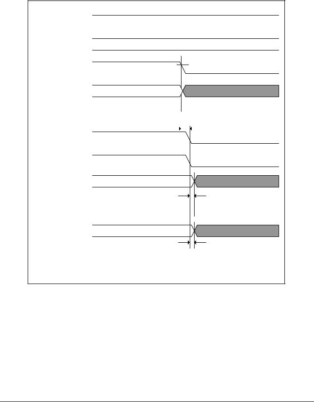
Figure 5-2: Valid Delay Timings
CLK |
VC |
VC |
|
TX |
TX |
|
V Valid |
Valid |
TPW
NOTES:
TX=T7 (Valid Delay)
TPW =T14 (Pulse W idth)
V=VREF for bus signal group; 1.0v for CMOS, Open-drain
VC= 1.25v
5-4 |
Electrical Specifications |
Section 5 |
Preliminary Information |
VIA Eden ESP Processor Datasheet |
|
January 2002 |
Figure 5-3: Setup and Hold Timings |
|
CLK
Signal
NOTES:
TS=T8 (Setup Time)
Th=T9 (Hold Time)
V=VREF for bus signals; 1.0v for CMOS VC= 1.25v
VC
TS Th
V Valid
Figure 5-4: Cold/Warm Reset and Configuration Timings
BCLK
RESET#
Configuration (A[15:5], BREQ0#, FLUSH#, INIT#
Bus outputs
Non-configuration
inputs
|
VC |
|
|
Tu |
|
|
Tt |
|
|
|
V |
Tv |
Tw |
Tx |
|
||
|
Valid |
|
|
|
Ty |
|
|
Valid |
|
|
Tz |
|
|
Active |
NOTES:
Tt=T9 (Bus Input Hold Time)
Tu=T8 (Bus Input Setup Time)
Tv=T10 (RESET# Pulse Width)
Tw=T16 (Reset Configuration Signals (A[15:5#, BREQ0#, FLUSH#, INIT#) Setup Time)
Tx=T17 (Reset Configuration Signals (A[15:5#, BREQ0#, FLUSH#, INIT#) Hold Time)
Ty=T18D (RESET# inactive to Valid Outputs)
Tz=T18E (RESET# inactive to Drive Signals)
VC=1.25v
Section 5 |
Electrical Specifications |
5-5 |

VIA Eden ESP Processor Datasheet |
Preliminary Information |
January 2002
Figure 5-5: Power-on Sequence and Reset Timings
BCLK
VTT
VID[4:0]/ |
Valid |
|
|
||||||||
BSEL[1:0] |
|
|
|||||||||
|
|
|
|
|
|
|
|
|
|
|
|
VREF |
|
|
|
|
|
|
|
|
|
|
|
VCC |
|
|
|
Ta |
|
|
|
|
|
|
|
PW RGOOD |
|
|
Tc |
|
|
VIH18,m in |
|
|
|||
|
|
|
|||||||||
|
|
|
|
|
|
||||||
|
|
|
|
|
|||||||
|
|
VIL18,m ax |
|
|
|||||||
RESET# |
|
|
|
|
|
|
|
Tb |
|
|
|
|
|
|
|
|
|
|
|
|
|
||
|
|
|
|
|
|
|
|
|
|||
|
|
|
|
|
|
|
|
|
|
|
|
|
|
|
|
|
|
|
|
|
|
|
|
NOTES:
Ta=T15 (PW RGOOD Inactive Pulse W idth)
Tb=T18 (RESET#/PW RGOOD Setup Time)
Tc=T18B (Setup time from VCC valid until PW RGOOD assertion)
5-6 |
Electrical Specifications |
Section 5 |
Preliminary Information |
VIA Eden ESP Processor Datasheet |
|
January 2002 |
Figure 5-6: Power Down Sequencing and Timings (VCC Leading)
VTT, VREF |
|
VID[4:0] |
|
BSEL[1:0] |
|
VCC |
VCC-12% |
BCLK |
Valid |
PW RGOOD |
|
|
|
|
|
|
|
Ta |
|
|
|
|
|
|
|
|
|||
|
|
|
|
|
|
VIL18 |
|||
RESET# |
|
|
|
|
|
|
|||
|
|
|
|
|
|
|
|
||
Bus Outputs |
Valid |
||||||||
Other CMOS Outputs |
|||||||||
|
|
|
|
|
|
|
|
||
Tb
All Inputs Valid
Tc
NOTES:
Ta=T19A (Time from VCC(nominal)-12% to PW RGOOD low)
Tb=T19B (All outputs valid after PW RGOOD low)
Tc=T19C (All inputs required valid after PW RGOOD low)
Section 5 |
Electrical Specifications |
5-7 |

VIA Eden ESP Processor Datasheet |
Preliminary Information |
January 2002
Figure 5-7: Power Down Sequencing and Timings (VTT Leading)
VTT, VREF |
|
|
VCC-12% |
|||
|
|
|
|
|
||
VID[4:0] |
Valid |
|||||
BSEL[1:0] |
||||||
|
|
|
|
|
||
VCC |
|
|
|
|
Ta, Tb, Tc |
|
BCLK |
|
|
|
|
||
|
|
|
||||
Valid |
||||||
PW RGOOD
RESET#
Bus Outputs |
Valid |
|
Other CMOS Outputs |
||
|
||
All Inputs |
Valid |
NOTES:
Ta=T20B (All outputs valid after VTT - 12%)
Tb=T20C (All inputs required valid after VTT - 12%)
Tc=T20D (VID, BSEL signals valid after VTT - 12%)
5-8 |
Electrical Specifications |
Section 5 |

Preliminary Information |
VIA Eden ESP Processor Datasheet |
January 2002
Figure 5-8: Stop Grant /Sleep Timing (BCLK Stopping Method)
|
Normal |
Stop Grant |
Sleep |
Stop Grant |
Normal |
BCLK |
|
|
Stopped |
|
|
|
|
Tv |
|
|
|
STPCLK# |
|
|
|
|
|
|
|
|
Tx |
Ty |
|
CPU bus |
stpgnt |
|
|
|
|
SLP# |
|
|
|
|
|
|
Tw |
|
|
Tz |
|
Compatibility |
Changing |
|
Frozen |
|
|
Signals |
|
|
|
||
|
|
|
|
|
NOTES:
Tv=T45 (Stop Grant Acknowledge Bus Cycle Completion to Clock Shut Off Delay)
Tw=T46 (Setup Time to Input Signal Hold Requirement)
Tx=T47 (Sleep PLL Lock Latency)
Ty=T48 (PLL lock to STPCLK# Hold Time)
Tz=T49 (Input Signal Hold Time)
Section 5 |
Electrical Specifications |
5-9 |